Biasing

Analog (Integrated) Circuit Design

12 Biasing

Biasing

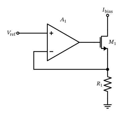
\[ I_\mathrm{bias} = \frac{V_\mathrm{ref}}{R_1}. \]

Biasing

Figure 64: A constant-current generator based on OTA.

Biasing

\[ V_\mathrm{bias} = R_2 I_\mathrm{bias} = \frac{R_2}{R_1} V_\mathrm{ref}. \]

12.1 Bandgap Reference

Bandgap Reference

\[ V_\mathrm{BE}\approx V_\mathrm{g0} \left( 1 - \frac{T}{T_0} \right) + V_\mathrm{BE0} \left( \frac{T}{T_0} \right) \tag{46}\]

\[ \Delta V_\mathrm{BE}= \frac{k T}{q} \ln \left( \frac{J_1}{J_2} \right) \tag{47}\]

Bandgap Reference

\[ V_\mathrm{ref} = V_\mathrm{g0} \left( 1 - \frac{T}{T_0} \right) + V_\mathrm{BE0} \left( \frac{T}{T_0} \right) + K \frac{k T}{q} \ln \left( \frac{J_1}{J_2} \right) \tag{48}\]

\[ K \frac{k}{q} \ln \left( \frac{J_1}{J_2} \right) = \frac{V_\mathrm{g0} - V_\mathrm{BE0}}{T_0}. \tag{49}\]

Bandgap Reference

\[ V_\mathrm{ref} = V_\mathrm{g0} \tag{50}\]

Bandgap Reference

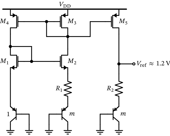
Figure 65: A simple bandgap reference.

Bandgap Reference
\[ \Delta V_\mathrm{BE}= \frac{k T}{q} \ln m \]

\[ I_\mathrm{bias} = \frac{\Delta V_\mathrm{BE}}{R_1} = \frac{1}{R_1} \frac{k T}{q} \ln m. \tag{51}\]

Bandgap Reference

\[ V_\mathrm{ref} = V_\mathrm{BE}+ \frac{R_2}{R_1} \frac{k T}{q} \ln m. \]

Bandgap Reference

Improved Bandgap Reference

For an improved implementation of Figure 65, the current mirrors should be cascoded, and a startup circuit should be included to guarantee proper operation after enabling it. Further, Equation 46 and Equation 47 build on the relationship \(I_\mathrm{C} = f(V_\mathrm{BE})\), while we control \(I_\mathrm{E}\) in this circuit. If \(\beta\) is large then \(I_\mathrm{C} \approx I_\mathrm{E}\), but this is not the case for the used PNPs.

Many more different bandgap architectures exist, with the Kuijk (Kuijk 1973) or the Brokaw (Brokaw 1974) types being popular choices.

Bandgap Reference

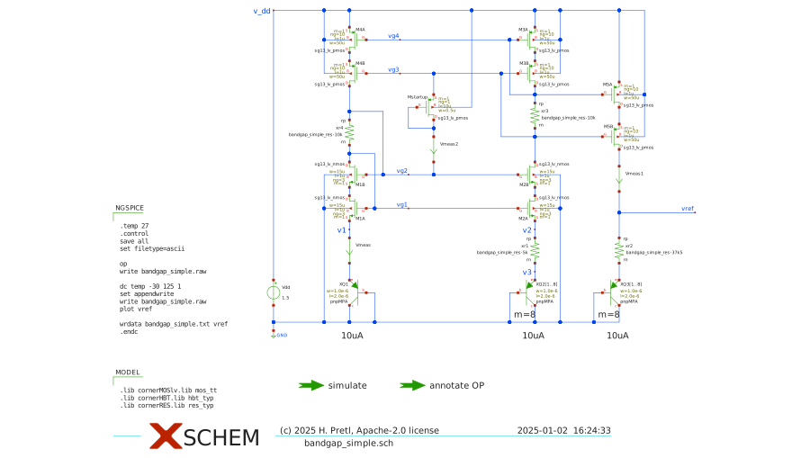
Figure 66: Simple bandgap reference circuit in Xschem.

Bandgap Reference

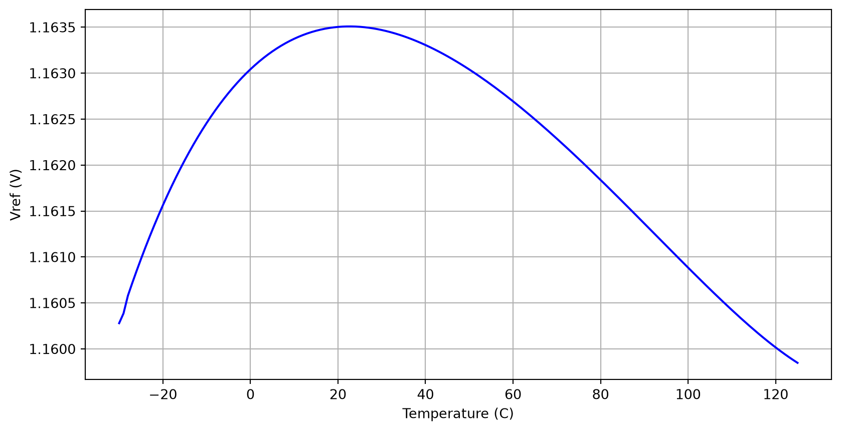
Figure 67: Reference voltage from simulated bandgap circuit.

12.2 Banba Bandgap Reference

Banba Bandgap Reference
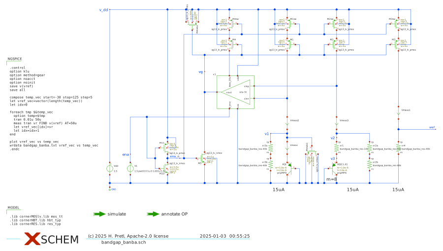
Figure 68: Banba bandgap reference circuit in Xschem.

Banba Bandgap Reference
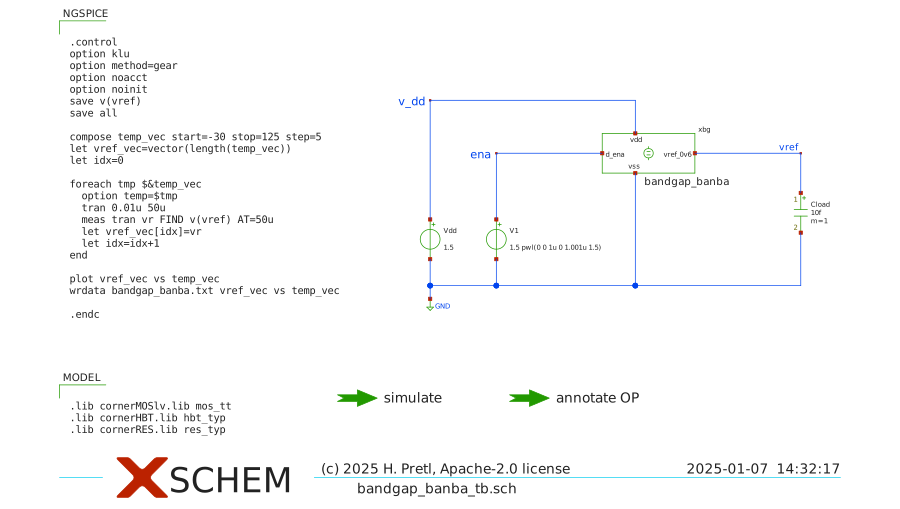
Figure 69: Banba bandgap testbench Xschem.

Banba Bandgap Reference
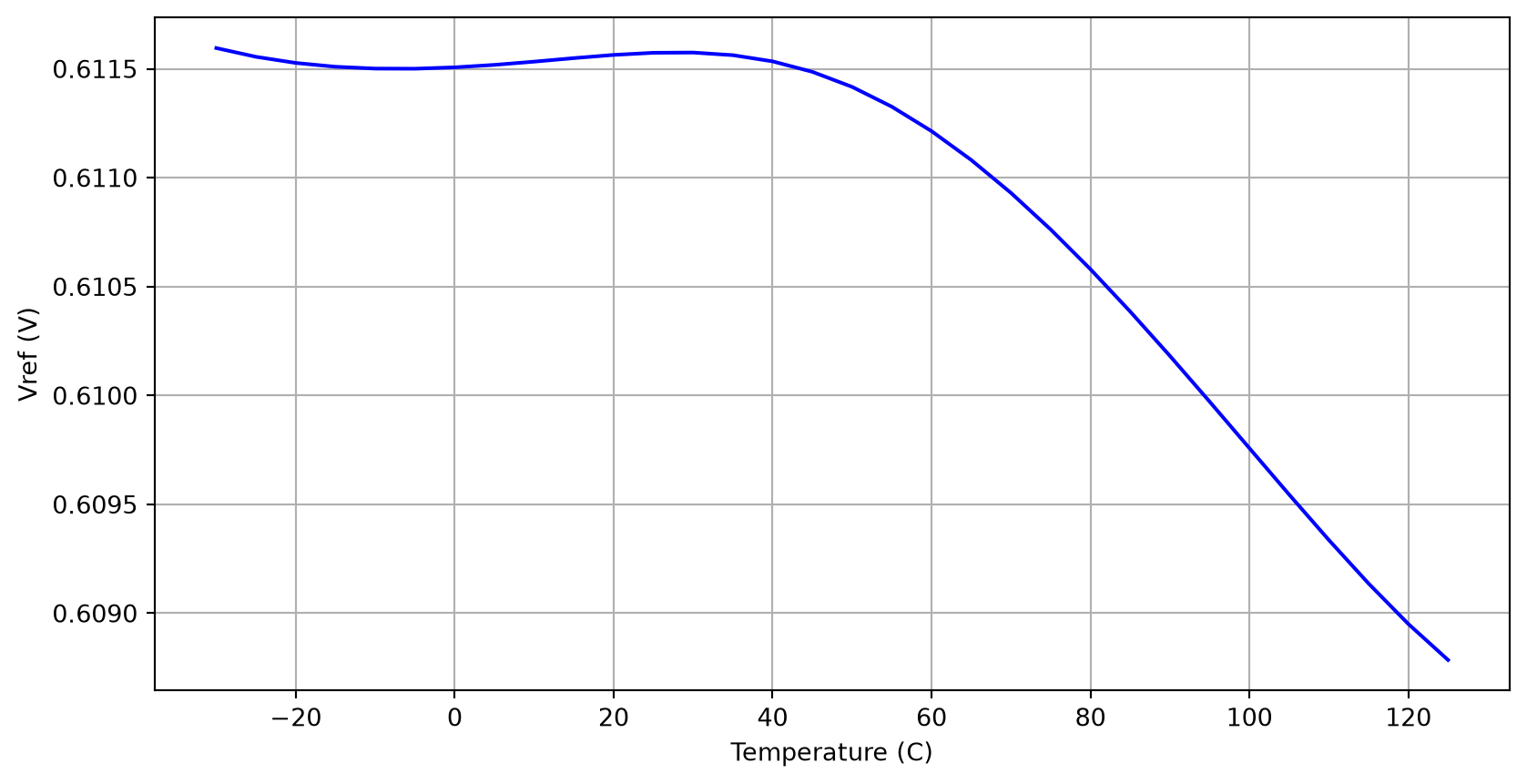
Figure 70: Reference voltage from simulated Banba bandgap circuit.

Banba Bandgap Reference

Exercise: Improved Low-Voltage Bandgap

As an optional exercise for advanced users: Design a bandgap circuit following (Razavi 2021). Implement the shown two-stage OTA and the regulated cascode.

As a starting point, the design of Section 12.2 can be used. As this design will contain more blocks, please build up a hierarchical design, with the OTAs designed in separate subcircuits.

References

Banba, H., H. Shiga, A. Umezawa, et al. 1999. “A CMOS Bandgap Reference Circuit with sub-1-V Operation.” IEEE Journal of Solid-State Circuits 34 (5): 670–74. https://doi.org/10.1109/4.760378.
Brokaw, A. P. 1974. A simple three-terminal IC bandgap reference.” IEEE Journal of Solid-State Circuits 9 (6): 388–93. https://doi.org/10.1109/JSSC.1974.1050532.
Eberlein, Matthias, Georgios Panagopoulos, and Harald Pretl. 2018. A 40nW, Sub-IV Truly ‘Digital’ Reverse Bandgap Reference Using Bulk-Diodes in 16nm FinFET.” 2018 IEEE Asian Solid-State Circuits Conference (A-SSCC), November, 99–102. https://doi.org/10.1109/asscc.2018.8579306.
Kuijk, K E. 1973. A precision reference voltage source.” IEEE Journal of Solid-State Circuits 8 (3): 222–26. https://doi.org/10.1109/JSSC.1973.1050378.
Razavi, Behzad. 2021. The Design of a Low-Voltage Bandgap Reference [The Analog Mind].” IEEE Solid-State Circuits Magazine 13 (3): 6–16. https://doi.org/10.1109/mssc.2021.3088963.
Widlar, R. J. 1971. New developments in IC voltage regulators.” IEEE Journal of Solid-State Circuits 6 (1): 2–7. https://doi.org/10.1109/jssc.1971.1050151.

References