Common-Source Amplifier
Analog (Integrated) Circuit Design
5 Common-Source Amplifier
Common-Source Amplifier
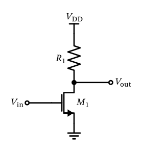
Figure 25: A MOSFET common-source amplifier with resistive load.
Common-Source Amplifier
\[ A_\mathrm{v} = \frac{V_\mathrm{out}}{V_\mathrm{in}} \approx - \frac{g_\mathrm{m}V_\mathrm{in} R_1}{V_\mathrm{in}} = - g_\mathrm{m}R_1. \]
Common-Source Amplifier
- voltage-to-current converter (MOSFET as common-source or common-gate; resistor),
- current-to-voltage converter (resistor),
- current-to-current converter (MOSFET as common-gate), and
- voltage-to-voltage converter (MOSFET as common-drain)
5.1 Sense Amplifier Driving 50 Ohm Matched Load
Sense Amplifier Driving 50 Ohm Matched Load
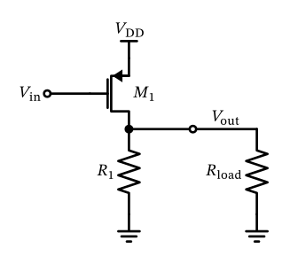
Figure 26: A MOSFET common-source amplifier with 50 Ohm load.
Sense Amplifier Driving 50 Ohm Matched Load
Exercise: PMOS-Based Measurement Amplifier
Please think about why exactly we want this measurement amplifier to be based on a PMOS instead of an NMOS.
Sense Amplifier Driving 50 Ohm Matched Load
Important 1: MOSFET Parameters NG and M
When sizing the MOSFET for this example we found that we need a fairly large \(W\), resulting in a MOSFET aspect ratio of \(W/L \gg 1000\). When constructing an integrated circuit out of individual MOSFETs, we strive for an overall IC dimension that is roughly square. For MOSFET with large aspect ratios we need to get them into a comfortable shape.
Sense Amplifier Driving 50 Ohm Matched Load
MOSFET Parameters NG and M
In order to achieve this, we construct the MOSFET out of smaller pieces, and the size of these pieces (called “gate fingers”) is controlled by the parameter ng. These MOSFET gate fingers all have the same \(L\), but their width is \(W_\mathrm{finger} = W / \text{ng}\). All these individual smaller MOSFETs are connected in parallel.
In order to increase the MOSFET model accuracy, often the maximum value of \(W_\mathrm{finger}\) is limited. In the case of SG13CMOS5L \(W_\mathrm{finger} \le 10\,\mu\text{m}\).
Sense Amplifier Driving 50 Ohm Matched Load
MOSFET Parameters NG and M
In order to construct even larger MOSFETs, we can connect multiple MOSFETs in parallel. We can do this in the circuit editor by placing and connecting these MOSFETs; but since this is often used there is a more convenient way: By using the parameter m (“multiplier” or “multiplicity”) we instantiate \(m\) MOSFETs connected in parallel.
Sense Amplifier Driving 50 Ohm Matched Load
MOSFET Parameters NG and M
When to use ng and when to use m? The use of ng results in a more compact IC layout, and is thus generally preferable. Only in certain instances (e.g., when using a really large \(W\)) m should be used. Further, the thoughtful use of ng allows one to construct all the NMOS and PMOS of a circuit out of the same gate finger elements. This will result in a very compact layout!
Sense Amplifier Driving 50 Ohm Matched Load
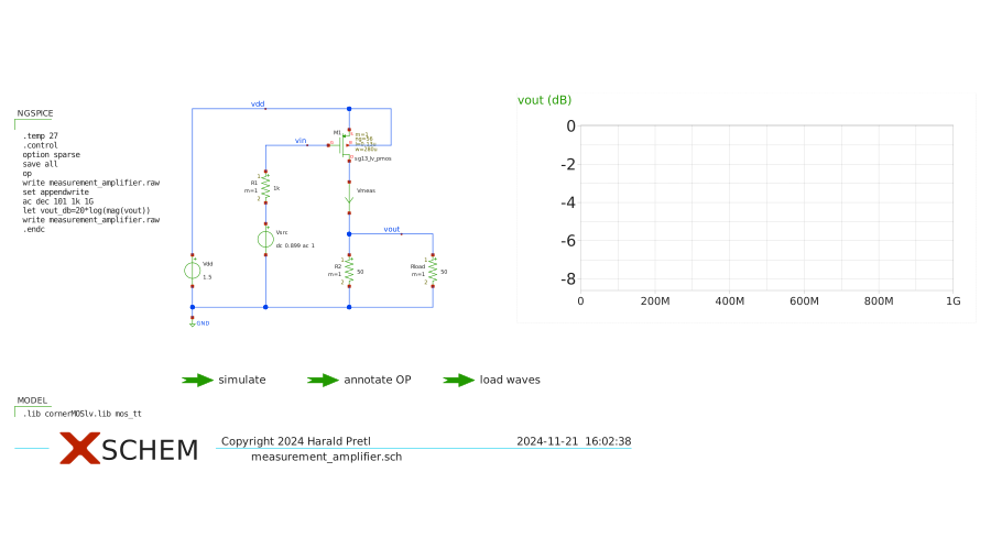
Exercise: Measurement Amplifier Simulation
Please go through the sizing notebook of the measurement amplifier and double-check the calculations. Do you agree that the calculations are correct?
Once you agree with the circuit sizing please build an Xschem simulation testbench where you simulate the small-signal voltage gain \(A_\mathrm{v}\) of this measurement amplifier if it is driven with an ideal voltage source. Keep in mind that the maximum MOSFET finger width is 10µm in this technology, so you need to set the parameter ng accordingly (see Important 1).
Sense Amplifier Driving 50 Ohm Matched Load
Exercise: Measurement Amplifier Simulation
- What is the dc gain of this amplifier when loaded with 50\(\Omega\)?
- The dc gain is likely not exactly 0 dB. Why is this so?
- Increase the width \(W\) of the PMOS until the gain is correct. What is the \(W\) that you had to set, and how much is \(I_\mathrm{D}\) now?
- What is the bandwidth (i.e., the -3 dB corner frequency) of the output voltage, when the voltage source has a source resistance of 1k\(\Omega\)?
Sense Amplifier Driving 50 Ohm Matched Load
Sense Amplifier Driving 50 Ohm Matched Load
Exercise: Measurement Amplifier Simulation