Improved Current Mirrors
Analog (Integrated) Circuit Design
10 Improved Current Mirrors
Improved Current Mirrors
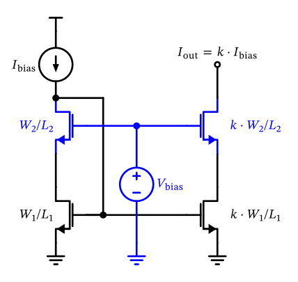
Figure 47: A cascoded current mirror using a biasing voltage to set the cascode gate potential.
Improved Current Mirrors
- Increased output resistance, as we have seen in Equation 34.
- Improved current mirroring accuracy, since the cascode transistors help to keep the drain-source voltage of the output transistor nearly constant and equal to that of the reference transistor.
Improved Current Mirrors
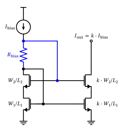
Figure 48: A high-swing cascoded current mirror.
Improved Current Mirrors
\[ r_\mathrm{out} = r_\mathrm{ds,casc} + r_\mathrm{ds} \cdot (1 + g_\mathrm{m,casc} \cdot r_\mathrm{ds,casc}). \tag{37}\]
Improved Current Mirrors
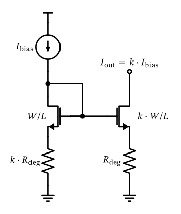
Figure 49: A current mirror with resistive degeneration.
Improved Current Mirrors
\[ r_\mathrm{out} = r_\mathrm{ds} + R_\mathrm{deg} \cdot (1 + g_\mathrm{m}\cdot r_\mathrm{ds}). \tag{38}\]
Improved Current Mirrors
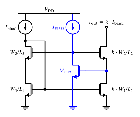
Figure 50: A regulated-cascode current mirror.
Improved Current Mirrors
\[ \begin{split} r_\mathrm{out} &= r_\mathrm{ds,casc} + r_\mathrm{ds} \cdot [1 + g_\mathrm{m,casc} \cdot r_\mathrm{ds,casc} \cdot (1 + g_\mathrm{maux} / g_\mathrm{dsaux})] \\ & \approx r_\mathrm{ds} \cdot g_\mathrm{m,casc} \cdot r_\mathrm{ds,casc} \cdot g_\mathrm{m,aux} \cdot r_\mathrm{ds,aux} \end{split} \tag{39}\]
Improved Current Mirrors
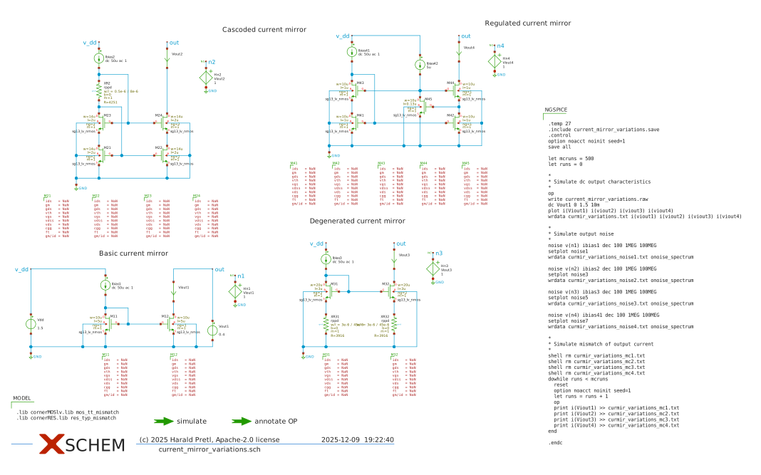
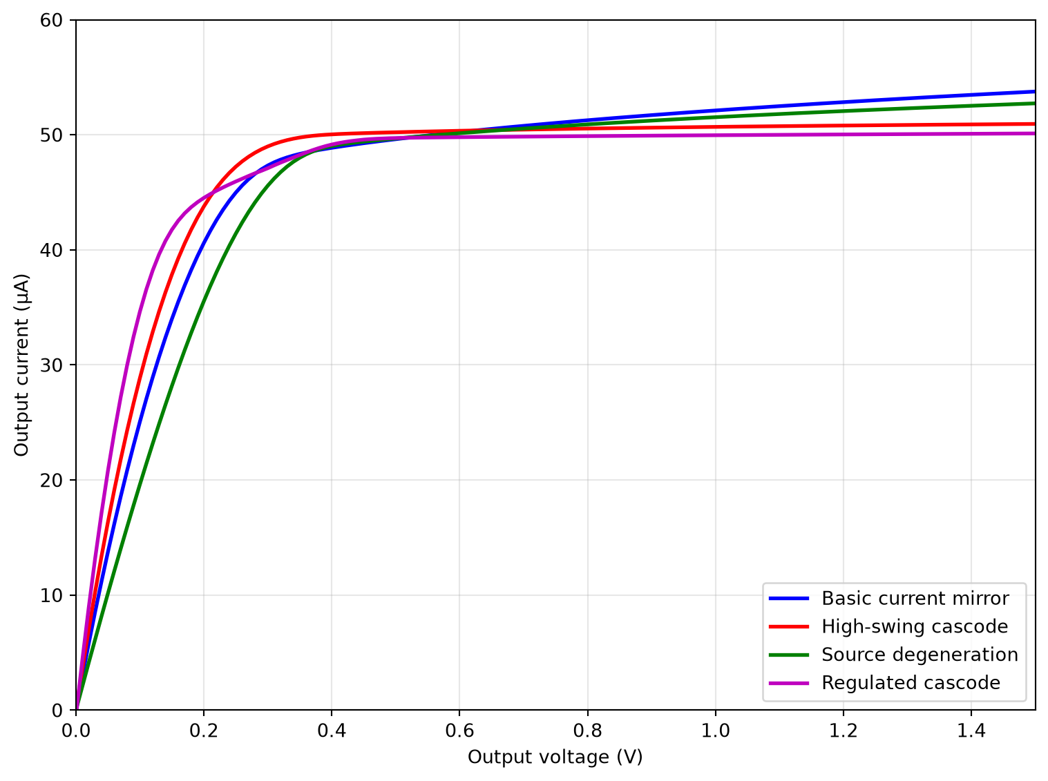
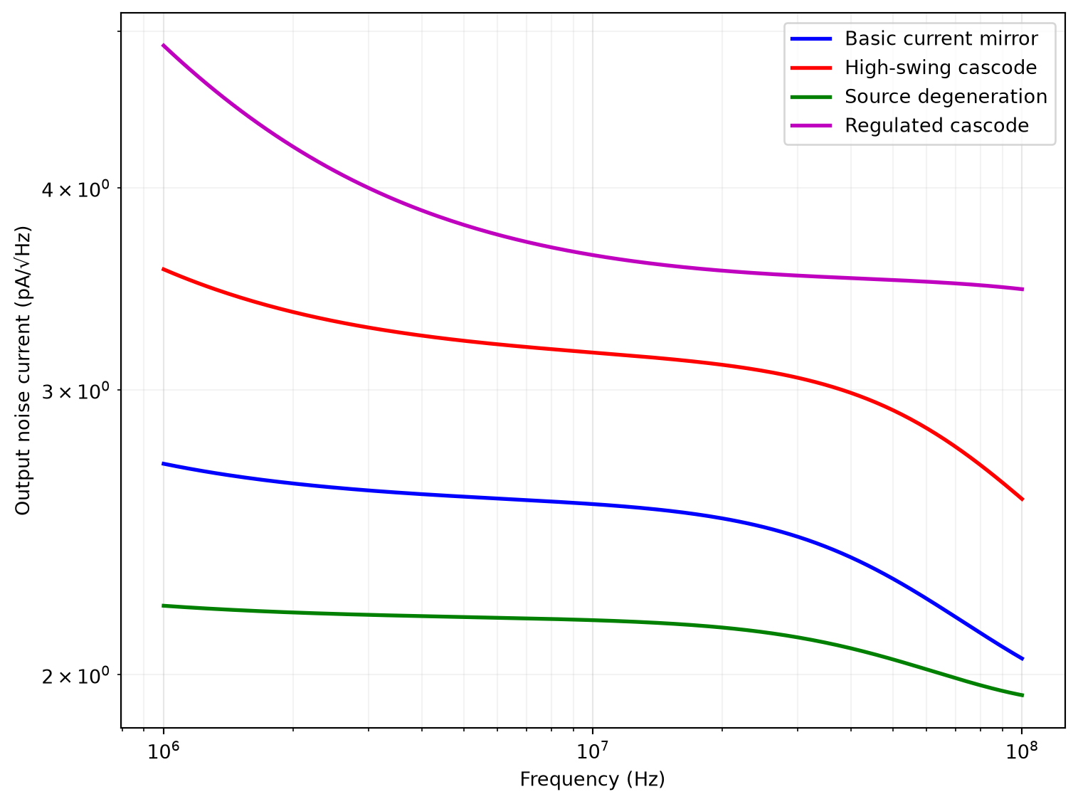
Figure 51: Simulation schematic of the improved current mirrors.
Improved Current Mirrors
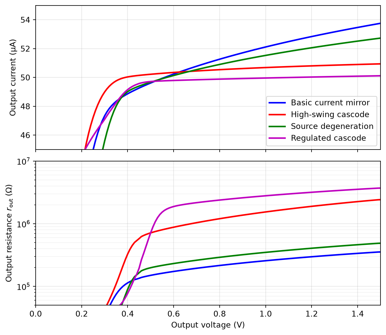
| Structure | \(r_\mathrm{out}\) at \(V_\mathrm{out} = 0.5\,\text{V}\) | at \(1.0\,\text{V}\) | at \(1.5\,\text{V}\) |
|---|---|---|---|
| Basic current mirror | \(150\,\text{k}\Omega\) | \(260\,\text{k}\Omega\) | \(360\,\text{k}\Omega\) |
| High-swing cascode | \(720\,\text{k}\Omega\) | \(1.5\,\text{M}\Omega\) | \(2.4\,\text{M}\Omega\) |
| Source degeneration | \(200\,\text{k}\Omega\) | \(350\,\text{k}\Omega\) | \(490\,\text{k}\Omega\) |
| Regulated cascode | \(710\,\text{k}\Omega\) | \(2.8\,\text{M}\Omega\) | \(3.7\,\text{M}\Omega\) |
Improved Current Mirrors
Improved Current Mirrors
Improved Current Mirrors
Improved Current Mirrors
10.1 Low-Voltage Regulated Current Mirror
Low-Voltage Regulated Current Mirror
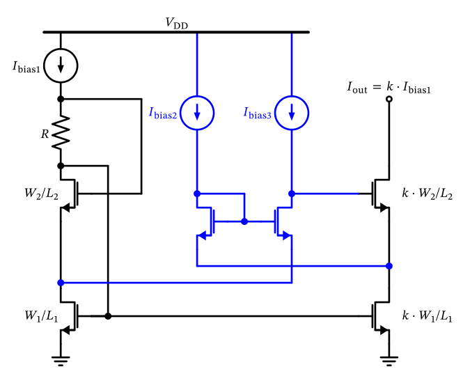
Figure 56: A low-voltage regulated-cascode current mirror.
10.2 Current Source Variations Summary
Current Source Variations Summary
- For general applications where output resistance and current accuracy are not critical, the basic current mirror can be used. It also has the lowest compliance voltage since only one transistor is stacked.
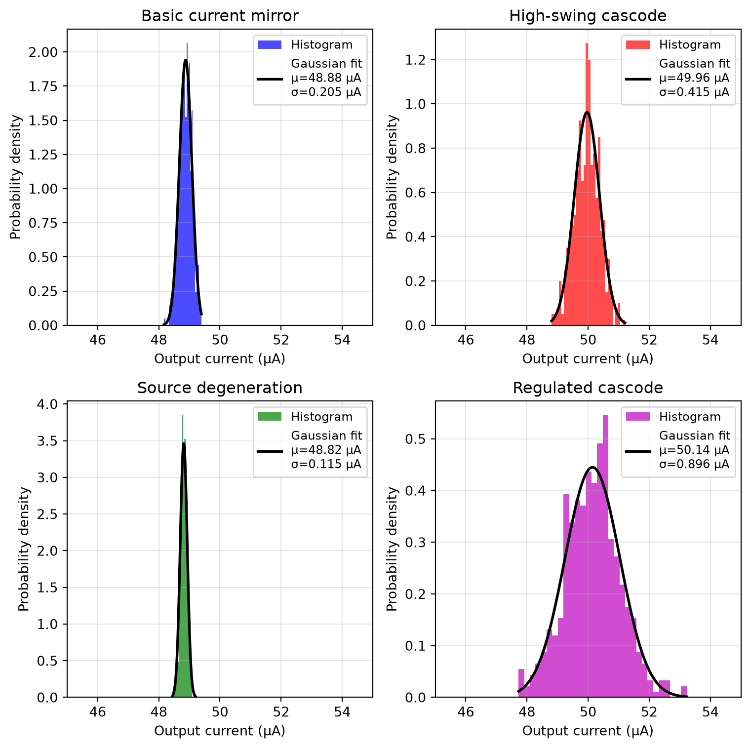
- The high-swing cascode current mirror is a good choice when higher output resistance is needed, while still keeping the circuit relatively simple. Be aware that the added cascode devices roughly double the current spread under mismatch compared to the basic mirror.
Current Source Variations Summary
- The source-degenerated current mirror is a good choice when the best current matching and low output noise are required. The additional voltage headroom that is dropped across the source degeneration can be adapted (higher is better), but a minimum value of 0.1 V should be used. Note that its output resistance is only mildly improved.
Current Source Variations Summary
- The regulated cascode current mirror is the best choice when the highest output resistance is required, and the additional complexity, output noise, and a roughly four-fold larger current spread under mismatch are acceptable.
- The low-voltage regulated cascode current mirror is a good alternative to the regulated cascode when a low compliance voltage is required.
10.3 Current Mirror Matching
Current Mirror Matching
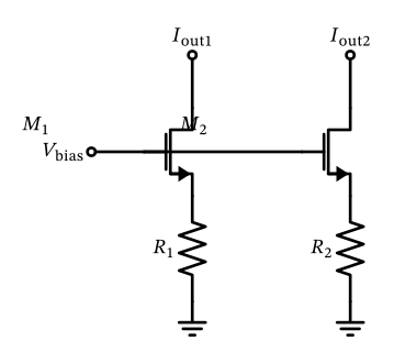
Figure 57: A current mirror pair with resistive degeneration.
Current Mirror Matching
\[ \begin{split} \sigma^2\left\{\frac{\Delta I_\mathrm{D}}{I_\mathrm{D}}\right\} & = \frac{\sigma^2\left\{\Delta V_\mathrm{th}\right\}}{(V_\mathrm{drv} + V_\mathrm{deg})^2} + \left( \frac{V_\mathrm{drv}}{V_\mathrm{drv} + V_\mathrm{deg}} \right)^2 \cdot \sigma^2\left\{\frac{\Delta K}{K}\right\} \\ & + \left( \frac{V_\mathrm{deg}}{V_\mathrm{drv} + V_\mathrm{deg}} \right)^2 \cdot \sigma^2\left\{\frac{\Delta R}{R}\right\}. \end{split} \tag{40}\]
Current Mirror Matching
\[ \begin{split} \sigma^2\left\{\frac{\Delta I_\mathrm{D}}{I_\mathrm{D}}\right\} & = \frac{\sigma^2\left\{\Delta V_\mathrm{th}\right\}}{[(g_\mathrm{m}/I_\mathrm{D})^{-1} + V_\mathrm{deg}]^2} + \left( \frac{1}{1 + V_\mathrm{deg}\cdot g_\mathrm{m}/I_\mathrm{D}} \right)^2 \cdot \sigma^2\left\{\frac{\Delta K}{K}\right\} \\ & + \left( \frac{V_\mathrm{deg} \cdot g_\mathrm{m}/I_\mathrm{D}}{1 + V_\mathrm{deg} \cdot g_\mathrm{m}/I_\mathrm{D}} \right)^2 \cdot \sigma^2\left\{\frac{\Delta R}{R}\right\}. \end{split} \tag{41}\]
Current Mirror Matching
\[ \sigma^2\left\{\frac{\Delta K}{K}\right\} = \sigma^2\left\{\Delta W\right\} \cdot \frac{1}{W^2} + \sigma^2\left\{\Delta L\right\} \cdot \frac{1}{L^2} + A_\mu^2 \cdot \frac{1}{W L}, \tag{42}\]
Current Mirror Matching
| Component | Matching Parameter | Value |
|---|---|---|
Resistor rsil |
\(\sigma\left\{\Delta R / R\right\} \cdot \sqrt{WL}\) | 1.2 % µm |
Resistor rppd |
\(\sigma\left\{\Delta R / R\right\} \cdot \sqrt{WL}\) | 1.5 % µm |
Resistor rhigh |
\(\sigma\left\{\Delta R / R\right\} \cdot \sqrt{WL}\) | 5 % µm |
MIM cap_cmim |
\(\sigma\left\{\Delta C / C\right\} \cdot \sqrt{WL}\) | 1 % µm (estimated) |
MOSFET sg13_lv_nmos |
\(\sigma\left\{\Delta V_\mathrm{th}\right\} \cdot \sqrt{WL}\) | 3.9 mV µm |
MOSFET sg13_lv_nmos |
\(\sigma\left\{\Delta W\right\}\) | 4 nm |
MOSFET sg13_lv_nmos |
\(\sigma\left\{\Delta L\right\}\) | 2 nm |
MOSFET sg13_lv_nmos |
\(\sigma\left\{\Delta \mu/\mu\right\} \cdot \sqrt{WL}\) | 0.5 % µm |
MOSFET sg13_lv_pmos |
\(\sigma\left\{\Delta V_\mathrm{th}\right\} \cdot \sqrt{WL}\) | 2.2 mV µm |
MOSFET sg13_lv_pmos |
\(\sigma\left\{\Delta W\right\}\) | 4 nm |
MOSFET sg13_lv_pmos |
\(\sigma\left\{\Delta L\right\}\) | 2 nm |
MOSFET sg13_lv_pmos |
\(\sigma\left\{\Delta \mu/\mu\right\} \cdot \sqrt{WL}\) | 0.33 % µm |
Current Mirror Matching
\[ \sigma^2\left\{\frac{\Delta I_\mathrm{D}}{I_\mathrm{D}}\right\} = \sigma^2\left\{\Delta V_\mathrm{th}\right\} \left( \frac{g_\mathrm{m}}{I_\mathrm{D}} \right)^2 + \sigma^2\left\{\frac{\Delta K}{K}\right\} \tag{43}\]
\[ \sigma^2\left\{\frac{\Delta I_\mathrm{D}}{I_\mathrm{D}}\right\} = \sigma^2\left\{\frac{\Delta R}{R}\right\} \tag{44}\]
Current Mirror Matching
Current Mirror Matching Calculation
Let us now calculate the current mirror matching of the simple current mirror. Using Equation 43, and using the sizing values of \(g_\mathrm{m}/ I_\mathrm{D}= 5\,\text{V}^{-1}\), \(W = 10\,\mu\text{m}\), and \(L = 5\,\mu\text{m}\), we can calculate the standard deviation of the transconductance parameter mismatch using Equation 42 and Table 4: \[ \sigma\left\{\frac{\Delta K}{K}\right\} = \sqrt{ \left( \frac{4\,\text{nm}}{10\,\mu\text{m}} \right)^2 + \left( \frac{2\,\text{nm}}{5\,\mu\text{m}} \right)^2 + \left( \frac{0.5\,\%\mu\text{m}}{\sqrt{10\,\mu\text{m} \cdot 5\,\mu\text{m}}} \right)^2 } = 0.09\,\%. \]
The standard deviation of the threshold voltage mismatch can be calculated using Equation 28 and Table 4: \[ \sigma\left\{\Delta V_\mathrm{th}\right\} = \frac{3.9\,\text{mV}\mu\text{m}}{\sqrt{10\,\mu\text{m} \cdot 5\,\mu\text{m}}} = 0.55\,\text{mV}. \]
Current Mirror Matching
Current Mirror Matching Calculation
Bringing both results into Equation 43, we get \[ \sigma\left\{\frac{\Delta I_\mathrm{D}}{I_\mathrm{D}}\right\} = \sqrt{ (0.55\,\text{mV} \cdot 5\,\text{V}^{-1})^2 + (0.09\,\%)^2} \approx 0.29\,\%. \] Comparing with the simulation results in Figure 54 for the basic current mirror, we can see that this gives a reasonable estimate compared to the standard deviation of about \(0.21\,\mu\text{A}/48.9\,\mu\text{A} = 0.43\,\%\) obtained from the Monte-Carlo simulation. The remaining discrepancy is due to simplifications in the analytical model (e.g., the square-law approximation).
Current Mirror Matching
Current Mirror Matching Calculation
Let us now calculate the current mirror matching of the resistively-degenerated current mirror. We can use Equation 41 to analyze this configuration. We use the sizing values of \(g_\mathrm{m}/ I_\mathrm{D}= 10\,\text{V}^{-1}\), \(W = 20\,\mu\text{m}\), and \(L = 3\,\mu\text{m}\), for the MOSFET, and \(V_\mathrm{deg} = 0.2\,\text{V}\), and \(W = 3\,\mu\text{m}\) / \(L = 45\,\mu\text{m}\) for the used rppd resistor (which at \(R_\square = 260\,\Omega\) gives the required \(R_\mathrm{deg} \approx 3.9\,\text{k}\Omega\)).
The standard deviation of the transconductance parameter mismatch can be calculated as \[ \sigma\left\{\frac{\Delta K}{K}\right\} = \sqrt{ \left( \frac{4\,\text{nm}}{20\,\mu\text{m}} \right)^2 + \left( \frac{2\,\text{nm}}{3\,\mu\text{m}} \right)^2 + \left( \frac{0.5\,\%\mu\text{m}}{\sqrt{20\,\mu\text{m} \cdot 3\,\mu\text{m}}} \right)^2 } = 0.09\,\%. \]
The standard deviation of the threshold voltage mismatch can be calculated as \[ \sigma\left\{\Delta V_\mathrm{th}\right\} = \frac{3.9\,\text{mV}\mu\text{m}}{\sqrt{20\,\mu\text{m} \cdot 3\,\mu\text{m}}} = 0.50\,\text{mV}. \]
Current Mirror Matching
Current Mirror Matching Calculation
The standard deviation of the resistor mismatch can be calculated using Equation 32 and Table 4: \[ \sigma\left\{\frac{\Delta R}{R}\right\} = \frac{1.5\,\%\mu\text{m}}{\sqrt{3\,\mu\text{m} \cdot 45\,\mu\text{m}}} = 0.13\,\%. \]
Plugging these results into Equation 41, we get \[ \begin{split} \sigma^2\left\{\frac{\Delta I_\mathrm{D}}{I_\mathrm{D}}\right\} =& \underbrace{\left( \frac{0.50\,\text{mV}}{0.1\,\text{V} + 0.2\,\text{V}} \right)^2}_{(0.17\,\%)^2} + \underbrace{\left( \frac{1}{1 + 0.2\,\text{V} \cdot 10\,\text{V}^{-1}} \cdot 0.09\,\% \right)^2}_{(0.03\,\%)^2} \\ & + \underbrace{\left( \frac{0.2\,\text{V} \cdot 10\,\text{V}^{-1}}{1 + 0.2\,\text{V} \cdot 10\,\text{V}^{-1}} \cdot 0.13\,\%\right)^2}_{(0.09\,\%)^2} \\ =& (0.19\,\%)^2. \end{split} \]
Current Mirror Matching
Current Mirror Matching Calculation
The three terms are worth reading individually. The degeneration has done its job on the MOSFET: the dominant threshold-voltage term is down to \(0.17\,\%\) and the transconductance-parameter term to a negligible \(0.03\,\%\), while the resistor contributes only \(0.09\,\%\). The total of \(0.19\,\%\) is a clear improvement over the \(0.29\,\%\) of the basic current mirror, and it matches the Monte-Carlo result in Figure 54 of about \(0.12\,\mu\text{A}/48.8\,\mu\text{A} = 0.24\,\%\) reasonably well.
Current Mirror Matching
Current Mirror Matching Calculation
The essential lesson of source degeneration is that it does not remove mismatch, it trades MOSFET mismatch for resistor mismatch — so the trade only pays off if the resistor is given enough area.
Current Mirror Matching
Current Mirror Matching Calculation
That is exactly why \(R_\mathrm{deg}\) is laid out here as a long, comparatively wide device (\(3 \times 45\,\mu\text{m}^2\)) instead of the minimum-width strip that would deliver the same \(3.9\,\text{k}\Omega\): a \(W = 1\,\mu\text{m}\) / \(L = 15\,\mu\text{m}\) resistor has the same resistance but nine times less area, which would raise its mismatch contribution from \(0.09\,\%\) to \(0.26\,\%\) and push the total back to \(0.31\,\%\) — no better than the basic mirror. Resistor area, not resistor value, is what buys the matching here.
References
Gray, Paul R., Paul J. Hurst, Stephen H. Lewis, and Robert G. Meyer. 2009. Analysis and Design of Analog Integrated Circuits. Wiley.
Hosticka, B. J. 1979. “Improvement of the gain of MOS amplifiers.” IEEE Journal of Solid-State Circuits 14 (6): 1111–14. https://doi.org/10.1109/jssc.1979.1051324.
Ivanov, Vadim V., and Igor M. Filanovsky. 2004. Operational Amplifier Speed and Accuracy Improvement. Kluwer Academic Publishers.