Current Mirror
Analog (Integrated) Circuit Design
6 Current Mirror
Current Mirror
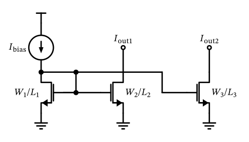
Figure 28: A current mirror with two output branches.
Current Mirror
Neglecting the impact of \(g_\mathrm{ds1}\) and \(g_\mathrm{ds2}\), the output current \(I_\mathrm{out1}\) is then given by \[ I_\mathrm{out1} \approx I_\mathrm{bias} \frac{W_2}{L_2} \frac{L_1}{W_1} \] and the output current \(I_\mathrm{out2}\) is given by \[ I_\mathrm{out2} \approx I_\mathrm{bias} \frac{W_3}{L_3} \frac{L_1}{W_1}. \]
Current Mirror: Key Points
- Output current set by the size ratio: \(I_\mathrm{out} \approx I_\mathrm{bias} \cdot \frac{W_2/L_2}{W_1/L_1}\)
- Any number of output branches (no gate current in MOSFETs)
- Build \(W\) and \(L\) from identical unit elements for good matching
- Main flaw: \(V_\mathrm{DS}\) of the diode (\(V_\mathrm{DS}= V_\mathrm{GS}\)) differs from the outputs
- Long \(L\) and low \(g_\mathrm{m}/I_\mathrm{D}\) give a flatter output current
Current Mirror
Exercise: Current Mirror
Please construct a current mirror based on the MOSFET-diode which we sized in Section 4. The input current \(I_\mathrm{bias} = 20\,\mu\text{A}\), and we want three output currents of size \(10\,\mu\text{A}\), \(20\,\mu\text{A}\), and \(40\,\mu\text{A}\).
Sweep the output voltage of all three current branches and see over which voltage range an acceptable current is created. For which output voltage range is the current departing from its ideal value, and why?
Current Mirror
Exercise: Current Mirror
You see that the slope of the output current is poor, as \(g_\mathrm{ds}\) is too large. We can improve this by changing the length to \(L = 5\,\mu\text{m}\) (for motivation, please look at the graphs in Section 3). In addition, for a current mirror we are not interested in a high \(g_\mathrm{m}/I_\mathrm{D}\) value, so we can use \(g_\mathrm{m}/I_\mathrm{D}= 5\) in this case. Please size the current mirror MOSFETs accordingly (please round the \(W\) to half micron, to keep sizes a bit more practical).