Differential Pair
Analog (Integrated) Circuit Design
7 Differential Pair
Differential Pair
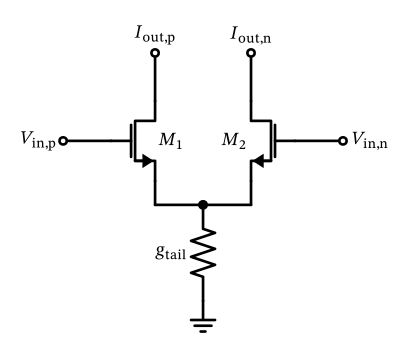
Figure 29: A differential pair.
Differential Pair
- a purely differential voltage, and
- a common-mode voltage,
7.1 Differential Operation of the Diffpair
Differential Operation of the Diffpair
The differential input voltage \(V_\mathrm{in} = V_\mathrm{in,p} - V_\mathrm{in,n}\), so that \[ V_\mathrm{in,p} = V_\mathrm{CM} + \frac{V_\mathrm{in}}{2} \] and \[ V_\mathrm{in,n} = V_\mathrm{CM} - \frac{V_\mathrm{in}}{2}. \]
The output current on each side is then given by (neglecting \(g_\mathrm{ds}\) and \(g_\mathrm{mb}\) of \(M_1\) and \(M_2\)) \[ I_\mathrm{out,p} = g_\mathrm{m1} \left( \frac{V_\mathrm{in}}{2} \right) \] and \[ I_\mathrm{out,n} = g_\mathrm{m2} \left( -\frac{V_\mathrm{in}}{2} \right). \]
Differential Operation of the Diffpair
The differential output current \(I_\mathrm{out}\) is then given by \[ I_\mathrm{out} = I_\mathrm{out,p} - I_\mathrm{out,n} = g_\mathrm{m}V_\mathrm{in} \tag{12}\]
7.2 Common-Mode Operation of the Diffpair
Common-Mode Operation of the Diffpair
If this is the case, then the output currents are not a function of the common-mode input voltage (\(I_\mathrm{tail}\) is set by the tail current source), and \[ I_\mathrm{out,p} = I_\mathrm{out,n} = I_\mathrm{out} = \frac{I_\mathrm{tail}}{2}. \]
Common-Mode Operation of the Diffpair
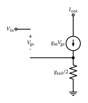
Figure 30: Small-signal model of the differential pair half-circuit in common-mode operation.
Common-Mode Operation of the Diffpair
Formulating KVL for the input-side loop we get \[ V_\mathrm{in} = V_\mathrm{gs}+ \frac{2 I_\mathrm{d}}{g_\mathrm{tail}}. \]
With \(I_\mathrm{out} = I_\mathrm{d}= g_\mathrm{m}V_\mathrm{gs}\) we arrive at \[ I_\mathrm{out} = \frac{g_\mathrm{m}\cdot g_\mathrm{tail}}{2 g_\mathrm{m}+ g_\mathrm{tail}} V_\mathrm{in} \tag{13}\]
Common-Mode Operation of the Diffpair
- If \(g_\mathrm{tail} = 0\) (ideal tail current source) then \(I_\mathrm{out} = 0\), the common-mode voltage variation from the input is suppressed and does not show up at the common-mode output current (which is constant due to the ideal tail current source). This is usually the case that we want to achieve.
Common-Mode Operation of the Diffpair
- If \(g_\mathrm{tail} \rightarrow \infty\) then \(I_\mathrm{out} = g_\mathrm{m}V_\mathrm{in}\), which means the output current is a function of the MOSFET \(g_\mathrm{m}\). If everything is perfectly matched, then the differential output current is zero, but the common-mode output current changes according to the common-mode input voltage. In special cases this can be a wanted behavior, this configuration is called a “pseudo-differential pair.”
- For the typical case that \(g_\mathrm{m}\gg g_\mathrm{tail}\) then \(I_\mathrm{out} \approx (g_\mathrm{tail}/2) V_\mathrm{in}\).
Common-Mode Operation of the Diffpair
\[ g_\mathrm{m}' = \frac{I_\mathrm{out}}{V_\mathrm{in}} = \frac{1}{g_\mathrm{m}^{-1} + R_\mathrm{degen}}. \]
Common-Mode Operation of the Diffpair
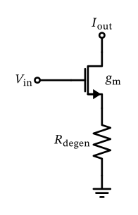
Figure 31: A MOSFET common-source amplifier with resistive degeneration.