First Steps
Analog (Integrated) Circuit Design
2 First Steps
2.1 The Metal-Oxide-Semiconductor Field-Effect-Transistor (MOSFET)
The Metal-Oxide-Semiconductor Field-Effect-Transistor (MOSFET)
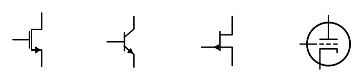
Figure 1: Circuit symbols for different voltage-controlled amplifiers (from left to right: MOSFET, bipolar junction transistor, junction FET, triode).
The Metal-Oxide-Semiconductor Field-Effect-Transistor (MOSFET)
MOSFET Background
Strictly speaking, the drain-source current of a MOSFET is controlled by the voltage between gate and bulk (\(V_\mathrm{GB}\)) and the voltage between drain and source (\(V_\mathrm{DS}\)). Since bulk is often connected to source anyway, and many circuit designers historically were already familiar with the operation of the bipolar junction transistor (BJT), it is common to consider the gate-source voltage (besides the drain-source voltage) as the controlling voltage.
The Metal-Oxide-Semiconductor Field-Effect-Transistor (MOSFET)
MOSFET Background
This focus on gate-source suggests that the source is special compared to the drain. In a typical physical MOSFET, however, the drain and source are constructed exactly the same (i.e., the MOSFET is a symmetric device), and which terminal is drain, and which terminal is source, is only determined by the applied voltage potentials, and can change dynamically during operation (think of a MOSFET operating as a switch… which side is the drain, which side is the source?).
The Metal-Oxide-Semiconductor Field-Effect-Transistor (MOSFET)
MOSFET Background
Unfortunately, this focus on a “special” source has made its way into some MOSFET compact models. The model that is used in SG13CMOS5L luckily uses the PSP model, which is formulated symmetrically with regards to drain and source, and is thus very well suited for analog and RF circuit design. For a detailed understanding of the PSP model please refer to the model documentation.
The Metal-Oxide-Semiconductor Field-Effect-Transistor (MOSFET)
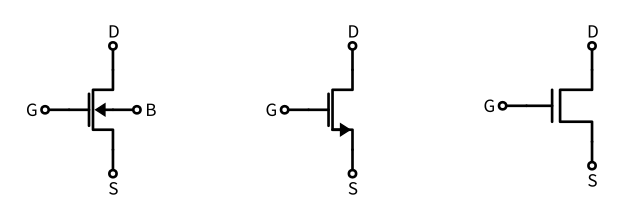
Figure 2: Circuit symbol of n-channel MOSFET.
The Metal-Oxide-Semiconductor Field-Effect-Transistor (MOSFET)
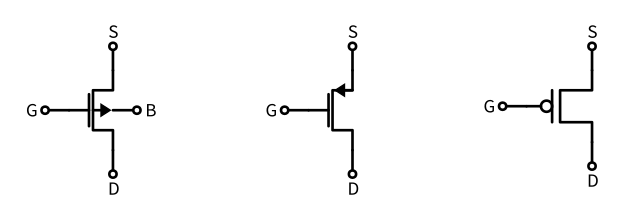
Figure 3: Circuit symbol of p-channel MOSFET.
The Metal-Oxide-Semiconductor Field-Effect-Transistor (MOSFET)
The Metal-Oxide-Semiconductor Field-Effect-Transistor (MOSFET)
MOSFET Symbol
This is a common “error” in many important textbooks and online resources (Razavi 2017; Gray et al. 2009; Sansen 2006), and it is important to be aware of this. The drain and source of a MOSFET are (usually) symmetric, and the current flow can be reversed by changing the applied voltages (and then also drain and source swap; generally, for an NMOS, the connection with the higher potential is the drain, the one with the lower potential is the source.
The Metal-Oxide-Semiconductor Field-Effect-Transistor (MOSFET)
MOSFET Symbol
For a PMOS, the situation is inverted).
The symbol in the middle of Figure 2 and Figure 3 is thus misleading, because is suggests that the source is special and that the current can only flow in one direction. This is not the case, and it is important to be aware of this when designing circuits, especially when using MOSFETs as switches.
The Metal-Oxide-Semiconductor Field-Effect-Transistor (MOSFET)
MOSFET Symbol
As many symbols are drawn this way, we will also use this symbol in this course (and the resemblance to a bipolar junction transistor is intentional), but please be aware of the fact that the drain and source are symmetric, and the current can flow in both directions depending on the bias voltages!
The Metal-Oxide-Semiconductor Field-Effect-Transistor (MOSFET)
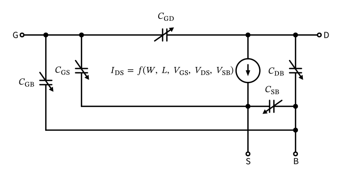
Figure 4: The MOSFET large-signal model.
The Metal-Oxide-Semiconductor Field-Effect-Transistor (MOSFET)
The Metal-Oxide-Semiconductor Field-Effect-Transistor (MOSFET)
Mathematical Notation
Throughout this material, we will largely stick to the following notation standardized by IEEE:
The Metal-Oxide-Semiconductor Field-Effect-Transistor (MOSFET)
Mathematical Notation
- A dc quantity is shown with an upper-case variable name with upper-case subscripts, like \(V_\mathrm{GS}\).
- Double-subscripts denote dc sources, like \(V_\mathrm{DD}\) and \(V_\mathrm{SS}\).
- An ac (small-signal) quantity (incremental quantity) has a lower-case variable name with a lower-case subscript, like \(g_\mathrm{m}\).
- A total quantity (dc plus ac) is shown as a lowercase variable name with upper-case subscript, like \(i_\mathrm{DS}\).
- An upper-case variable name with a lower-case subscript is used to denote signal amplitudes (phasors), like \(V_\mathrm{gs}\), \(V_\mathrm{ds}\), \(I_\mathrm{d}\).
The Metal-Oxide-Semiconductor Field-Effect-Transistor (MOSFET)
A Comment on Active and Passive Devices and Linear vs. Nonlinear
In contrast to the passive devices resistor \(R\), inductor \(L\), and capacitor \(C\), which can only dissipate energy (and are often treated in a linearized fashion), transistors (like the MOSFET) are called “active”, since they can provide signal power amplification. However, transistors can not create energy out of thin air, but merely convert dc energy (supplied by the power supply) into ac energy (Manley and Rowe 1956).
The Metal-Oxide-Semiconductor Field-Effect-Transistor (MOSFET)
A Comment on Active and Passive Devices and Linear vs. Nonlinear
They have to have nonlinear transfer characteristics to do this, but it has been shown that a piecewise-linear characteristic is sufficient (Jakoby 2022). This is very good news for circuit design, as usually we strive for linear behaviour!
2.1.1 Large-Signal MOSFET Model
Large-Signal MOSFET Model
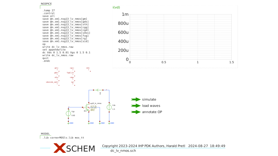
Figure 5: Testbench for NMOS dc sweeps.
Large-Signal MOSFET Model
MOSFET Simulation Model
For modelling the MOSFET behavior in a circuit simulator like ngspice different models are available. Some of these models have been widely adopted, like the BSIM (Berkeley Short-channel IGFET Model) or PSP (Philips Penn State) model. The PSP model version 103.6 is used in the IHP SG13CMOS5L PDK for the LV and HV MOSFET. This model has several advantages:
Large-Signal MOSFET Model
MOSFET Simulation Model
- Physics-based surface-potential model
- Symmetric formulation with respect to drain and source
- Support for mobility reduction, velocity saturation, DIBL, gate current, lateral doping gradient effects, STI stress, NQS, etc.
The PSP 103.6 model documentation can be found here. In chapter 8 the dc operating point output of the model (these parameters can be queried in ngspice) is explained, which is helpful to interpret the simulation output.
Large-Signal MOSFET Model
Exercise: MOSFET Investigation
Please try to execute the following steps and answer these questions:
- Get the LV NMOS testbench (available at https://github.com/iic-jku/analog-circuit-design/blob/main/xschem/dc_lv_nmos.sch) working in your IIC-OSIC-TOOLS environment.
- Make yourself familiar with Xschem (change the schematic in various ways, run a simulation, graph the result).
- Make yourself familiar with ngspice (run various simulations, save nets and parameters, use the embedded Xschem graphing, explore the interactive ngspice shell to look at MOSFET model parameters).
Large-Signal MOSFET Model
Exercise: MOSFET Investigation
- Explore the LV NMOS
sg13_lv_nmos:- How is \(I_\mathrm{D}\) affected by \(V_\mathrm{GS}\) and \(V_\mathrm{DS}\)?
- Change \(W\) and \(L\) of the MOSFET. What is the impact on the above parameters? Can you explain the variations?
- Look at the capacitance values for \(C_\mathrm{GS}\), \(C_\mathrm{GB}\), \(C_\mathrm{GD}\), and \(C_\mathrm{DB}\). How are they affected by \(W\) and \(L\) and by changing the bias conditions (play with \(V_\mathrm{GS}\) and \(V_\mathrm{DS}\))?
Large-Signal MOSFET Model
Exercise: MOSFET Investigation
- Explore the LV NMOS
sg13_lv_nmos:- When looking at the model parameters in ngspice, you see that there is a \(C_\mathrm{GD}\) and a \(C_\mathrm{DG}\). Why is this, what could be the difference? Sometimes these capacitors show a negative value, why? (Hint: Study Note 1)
Large-Signal MOSFET Model
Exercise: MOSFET Investigation
- Build testbenches in Xschem for the LV PMOS, the HV NMOS, and the HV PMOS. Explore the different results.
- For a given \(W\) and \(L\), which device provides more drain current? How are the capacitances related?
- If you would have to size an inverter, what would be the ideal ratio of \(W_p/W_n\)? Will you exactly design this ratio, or are the reasons to deviate?
Large-Signal MOSFET Model
Exercise: MOSFET Investigation
- Build testbenches in Xschem for the LV PMOS, the HV NMOS, and the HV PMOS. Explore the different results.
- There are LV and HV MOSFETs, and you investigated the difference in performance. What is the rationale when designing circuits for selection either an LV type, and when to choose an HV type?
- Build a test bench to explore the body effect, start with LV NMOS.
- What happens when \(V_\mathrm{SB}\neq 0\)?
2.1.2 Small-Signal MOSFET Model
\[ g_\mathrm{m}= \frac{\partial I_\mathrm{D}(V_\mathrm{GS}, V_\mathrm{DS}, V_\mathrm{SB})}{\partial V_\mathrm{GS}}, \]
\[ g_\mathrm{ds}= \frac{\partial I_\mathrm{D}(V_\mathrm{GS}, V_\mathrm{DS}, V_\mathrm{SB})}{\partial V_\mathrm{DS}} \]
Small-Signal MOSFET Model
\[ g_\mathrm{mb}= -\frac{\partial I_\mathrm{D}(V_\mathrm{GS}, V_\mathrm{DS}, V_\mathrm{SB})}{\partial V_\mathrm{SB}} = \frac{\partial I_\mathrm{D}(V_\mathrm{GS}, V_\mathrm{DS}, V_\mathrm{BS})}{\partial V_\mathrm{BS}} \]
Small-Signal MOSFET Model
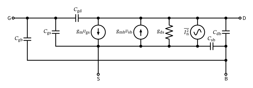
Figure 6: The MOSFET small-signal model.
Small-Signal MOSFET Model
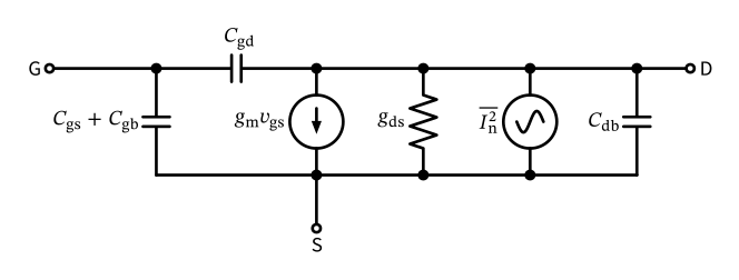
Figure 7: The MOSFET small-signal model when source and bulk are shorted.
Small-Signal MOSFET Model
\[ \overline{I_\mathrm{n}^2} = 4 k T \gamma g_\mathrm{d0}, \tag{1}\]
Small-Signal MOSFET Model
MOSFET Triode and Saturation Region
Sometimes we will refer to different operating modes of the MOSFET like “saturation” or “triode.” Generally speaking, when the drain-source voltage is small, then the MOSFET acts as a voltage-controlled resistor (since the impact of both \(V_\mathrm{GS}\) and \(V_\mathrm{DS}\) on \(I_\mathrm{D}\) is large), and this mode of operation we call “triode” mode.
Small-Signal MOSFET Model
MOSFET Triode and Saturation Region
When the drain-source voltage \(V_\mathrm{DS}\) is increased, at some point the drain-source current saturates and is only a weak function of the drain-source voltage, while still being well controlled by \(V_\mathrm{GS}\). This mode is called “saturation” mode.
Small-Signal MOSFET Model
MOSFET Triode and Saturation Region
As you can see in the large-signal investigations, these transitions happen gradually, and it is difficult to define a precise point where one operating mode switches to the other one. In this sense we use terms like “triode” and “saturation” only in an approximate sense.
Small-Signal MOSFET Model
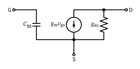
Figure 8: The MOSFET small-signal basic pi-model.
Small-Signal MOSFET Model
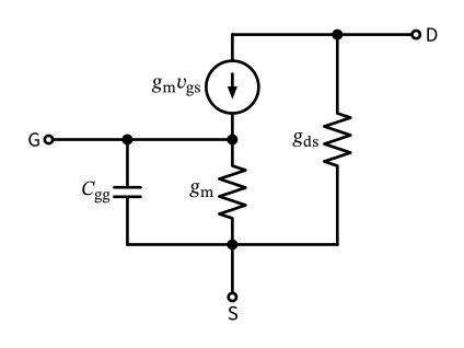
Figure 9: The MOSFET small-signal basic T-model.
Small-Signal MOSFET Model
Small-Signal MOSFET Model
It can easily be derived using the simplified MOSFET small-signal model of Figure 7 by driving it with a voltage source and shorting the output to ground (neglecting the feed-forward current introduced by \(C_\mathrm{gd}\)): \[ \omega_\mathrm{T} = 2 \pi f_\mathrm{T} \approx \frac{g_\mathrm{m}}{C_\mathrm{gg}} = \frac{g_\mathrm{m}}{C_\mathrm{gs}+ C_\mathrm{gd}+ C_\mathrm{gb}}. \tag{2}\]
Small-Signal MOSFET Model
Exercise: MOSFET Transit Frequency
As a home exercise, try to derive Equation 2 starting from Figure 7. This is a useful exercise to verify your understanding of the small-signal model.
Small-Signal MOSFET Model
Exercise: MOSFET Small-Signal Parameters
Please try to execute the following steps and answer the following questions:
Small-Signal MOSFET Model
Exercise: MOSFET Small-Signal Parameters
- Reuse the LV NMOS testbench (available at https://github.com/iic-jku/analog-circuit-design/blob/main/xschem/dc_lv_nmos.sch).
- Explore the LV NMOS
sg13_lv_nmos:- How are \(g_\mathrm{m}\) and \(g_\mathrm{ds}\) changing when you change the dc node voltages?
- What is the ratio of \(g_\mathrm{m}\) to \(g_\mathrm{mb}\)? What is the physical reason behind this ratio (you might want to revisit MOSFET device physics at this point)?
- Take a look at the device capacitances \(C_\mathrm{gs}\), \(C_\mathrm{gd}\), and \(C_\mathrm{gb}\). Why are they important? What is the \(f_\mathrm{T}\) of the MOSFET?
Small-Signal MOSFET Model
Exercise: MOSFET Small-Signal Parameters
- Explore the LV NMOS
sg13_lv_nmos:- Look at the drain noise current according to the MOSFET model and compare with a hand calculation of the noise. In the noise equation there is the factor \(\gamma\), which in triode is \(\gamma=1\) and in saturation is \(\gamma=2/3\) according to basic text books. Which value of \(\gamma\) are you calculating? Why might it be different?
Small-Signal MOSFET Model
Exercise: MOSFET Small-Signal Parameters
- Go back to your testbench for the LV PMOS
sg13_lv_pmos:- What is the difference in \(g_\mathrm{m}\), \(g_\mathrm{ds}\), and other parameters between the NMOS and the PMOS? Why could they be different?
Small-Signal MOSFET Model
Note 1: Maxwell Capacitance Matrix
A Maxwell capacitance matrix (Maxwell 1873) provides the relation between voltages on a set of conductors and the charges on these conductors. For a given conductor set with \(N\) conductors (and thus \(N\) terminals) the relation is \[ \mathbf{Q} = \mathbf{C} \cdot \mathbf{V} \] where \(\mathbf{Q}\) is a vector of the charges on the \(N\) conductors, \(\mathbf{C}\) is a \(N \times N\) capacitance matrix, and \(\mathbf{V}\) is the potential vector.
Small-Signal MOSFET Model
Maxwell Capacitance Matrix
In the case of two conductors and physical capacitances between them, \(\mathbf{C}\) is given by \[ \mathbf{C} = \begin{pmatrix} C_{11} + C_{12} & -C_{12} \\ -C_{12} & C_{12} + C_{22} \\ \end{pmatrix} \] where \(C_{11}\) and \(C_{22}\) are the auto capacitances of the conductors towards infinity (ground), and \(C_{12} = C_{21}\) is the mutual capacitance between the two conductors. Note that these are the physical capacitances, and that they are therefore not identical to the entries of \(\mathbf{C}\): a diagonal entry of \(\mathbf{C}\) is the sum of all capacitances touching a node (\(\partial Q_1 / \partial V_1 = C_{11} + C_{12}\)), whereas an off-diagonal entry is negative (\(\partial Q_1 / \partial V_2 = -C_{12}\)).
Small-Signal MOSFET Model
Maxwell Capacitance Matrix
Using the above equation to calculate \(Q_1\) (the charge on conductor \(1\)) results in \[ Q_1 = ( C_{11} + C_{12} ) V_1 - C_{12} V_2 = C_{11} (V_1 - 0) + C_{12} (V_1 - V_2) \] which is the expected result.
Such a Maxwell capacitance formulation is also used in the MOSFET model to describe the charge at a terminal as a function of potential at another terminal. So, \[ C_\mathrm{GD}= \frac{\partial Q_\mathrm{G}}{\partial V_\mathrm{D}} \] or \[ C_\mathrm{GG}= \frac{\partial Q_\mathrm{G}}{\partial V_\mathrm{G}} \] with \(Q_\mathrm{G}\) the charge at terminal G in response to either \(V_\mathrm{D}\) or \(V_\mathrm{G}\). Note that in a MOSFET, generally \(C_{xy} \ne C_{yx}\)!
Small-Signal MOSFET Model
Maxwell Capacitance Matrix
This also explains the negative capacitance values that a simulator sometimes reports (see the exercise above): the off-diagonal entries of a Maxwell capacitance matrix carry a negative sign by construction, so a reported \(C_\mathrm{GD}\) of, e.g., \(-1\,\text{fF}\) simply means a physical coupling capacitance of \(1\,\text{fF}\) between gate and drain.