# read table data
from pygmid import Lookup as lk
import numpy as np
lv_nmos = lk('sg13_lv_nmos.mat')
lv_pmos = lk('sg13_lv_pmos.mat')
# list of parameters: VGS, VDS, VSB, L, W, NFING, ID, VT, GM, GMB, GDS, CGG, CGB, CGD, CGS, CDD, CSS, STH, SFL
# if not specified, minimum L, VDS=max(vgs)/2=0.9 and VSB=0 are used A Basic 5-Transistor OTA
Analog (Integrated) Circuit Design
8 A Basic 5-Transistor OTA
A Basic 5-Transistor OTA
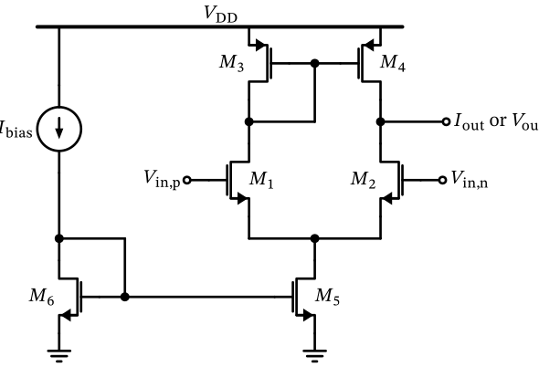
Figure 32: The 5-transistor OTA.
A Basic 5-Transistor OTA
Refresh MOSFET Basic Circuits
While we repeat the basics of elementary MOSFET amplifier stages (like common-source stage, common-gate stage, and current mirror) in this course material, the following compendium (Murmann 2013) is recommended for review. It is freely available at https://github.com/bmurmann/Book-on-MOS-stages.
In addition, we can highly recommend these references (Gray et al. 2009; Razavi 2017) for further study.
OPA vs. OTA
| OPA | OTA | |
|---|---|---|
| Input impedance | \(\infty\) | \(\infty\) |
| Output resistance | \(0\) (voltage output) | \(\infty\) (current output) |
| Ideal gain | \(A_\mathrm{v} \rightarrow \infty\) | \(G \rightarrow \infty\) |
- With a capacitive (high-ohmic) load, an OTA acts as a high-gain voltage amplifier
- An OTA is simpler — the simplest circuit that does the job is usually best
8.1 Voltage Buffer with OTA
Voltage Buffer with OTA
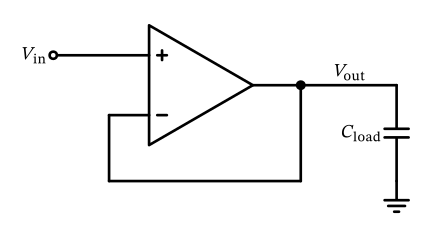
Figure 33: A voltage buffer (based on OTA) driving a capacitive load.
Voltage Buffer with OTA
| Specification | Value | Unit |
|---|---|---|
| Supply voltage | \(1.45 < \underline{1.5} < 1.55\) | V |
| Temperature range (industrial) | \(-40 < \underline{27} < 125\) | degC |
| Load capacitance \(C_\mathrm{load}\) | \(50\) | fF |
| Input voltage range (for buffering 2/3 bandgap voltage) | \(0.7 < \underline{0.8} < 0.9\) | V |
| Signal bandwidth (3 dB) | \(>10\) | MHz |
| Output voltage error | \(<3\) | % |
| Total output noise (rms) | \(<1\) | mVrms |
| Supply current (as low as possible) | \(<10\) | µA |
| Stability | stable for rated \(C_\mathrm{load}\) | |
| Turn-on time (settled to with 1%) | \(<10\) | µs |
| Externally provided bias current (nominal) | \(20\) | µA |
8.2 Large-Signal Analysis of the OTA
Large-Signal Analysis of the OTA
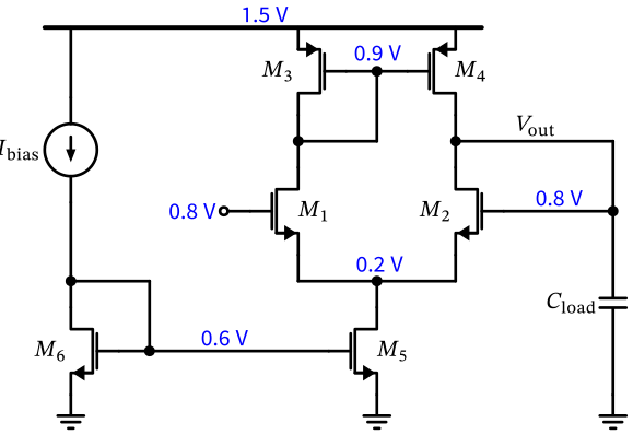
Figure 34: The 5-transistor OTA with external connections and load capacitor.
Large-Signal Analysis of the OTA
- When the input is at its maximum of \(0.9\,\text{V}\), we see that we need to keep \(M_1\) in saturation. We can calculate that \(V_\mathrm{DS1} = V_\mathrm{DD}- |V_\mathrm{GS3}| + V_\mathrm{GS1} - V_\mathrm{in} = 1.45 - 0.6 + 0.6 - 0.9 = 0.55\,\text{V}\), which leaves enough margin.
- When the input is at its minimum of \(0.7\,\text{V}\), we see that the \(V_\mathrm{DS5}\) of \(M_5\) is calculated as \(V_\mathrm{DS5} = V_\mathrm{in} - V_\mathrm{GS1} = 0.7 - 0.6 = 0.1\,\text{V}\), so this leaves little margin, but we can make \(V_\mathrm{GS1}\) smaller, so it should work out.
- For the output voltage, when the output voltage is on the high side, it leaves \(|V_\mathrm{DS4}| = V_\mathrm{DD}- V_\mathrm{out} = 1.45 - 0.9 = 0.55\,\text{V}\), which is enough margin.
Large-Signal Analysis of the OTA
\[ T_\mathrm{slew} \approx \frac{C_\mathrm{load} \cdot V_\mathrm{out,max}}{I_\mathrm{tail}} = \frac{50 \cdot 10^{-15} \cdot 0.9}{10 \cdot 10^{-6}} = 4.5\,\text{ns}. \]
The small-signal settling (assuming one pole at the bandwidth corner frequency) leads to an approximate settling time (1% error corresponds to \(\approx 5 \tau\)) of \[ T_\mathrm{settle} \approx \frac{5}{2 \pi f_\mathrm{c}} = \frac{5}{2 \pi \cdot 10 \times 10^{6}} = 0.08\,\mu\text{s}. \]
8.3 Small-Signal Analysis of the OTA
Small-Signal Analysis of the OTA
- dc voltage gain \(A_0\)
- gain-bandwidth product (GBW)
- output noise
Small-Signal Analysis of the OTA
For a voltage follower in the configuration shown in Figure 33 the voltage gain is given by (see Figure 33) \[ (V_\mathrm{in} - V_\mathrm{out}) \cdot A_0 = V_\mathrm{out} \to \frac{V_\mathrm{out}}{V_\mathrm{in}} = \frac{A_0}{1 + A_0}. \tag{14}\]
Small-Signal Analysis of the OTA
Small-Signal vs. Large-Signal Operation
In order to get the correct dc voltage per the specification we require the large-signal gain calculated with Equation 14. However, calculating the large-signal gain of a circuit is quite involved (usually mandating the use of a large-signal nonlinear model for the used components), so we typically resort to do a simpler small-signal calculation instead, like in Section 8.3. We deliberately introduce this error, but we should not get confused about the difference between large- and small-signal operation!
8.3.1 OTA Small-Signal Transfer Function
- We assume that \(g_\mathrm{m1,2} = g_\mathrm{m1} = g_\mathrm{m2}\), \(g_\mathrm{m3,4} = g_\mathrm{m3} = g_\mathrm{m4}\), and \(C_\mathrm{gs3,4} = C_\mathrm{gs3} = C_\mathrm{gs4}\) for symmetry reasons (as \(M_1\) and \(M_2\) will have to be equally sized, as well as \(M_3\) and \(M_4\)).
- We will set \(g_\mathrm{mb}= 0\) for all MOSFETs.
OTA Small-Signal Transfer Function
- We will further set \(C_\mathrm{gd}= 0\) for all MOSFETs except for \(M_4\) where we expect a Miller effect on this capacitor, and we could add its effect by increasing the capacitance at the gate node of \(M_{3,4}\) (for background please see Section 17.1). However, as this does not create a dominant pole in this circuit, we consider this a minor effect (see Equation 17). Thus, only \(2C_\mathrm{gs3,4}\) is considered at the gate node of the current mirror load.
OTA Small-Signal Transfer Function
- We assume \(g_\mathrm{m}\gg g_\mathrm{ds}\), so we set \(g_\mathrm{ds1} = g_\mathrm{ds3} = 0\) as this node is dominated by \(g_\mathrm{m3}^{-1}\).
- The drain capacitance of \(M_2\) and \(M_4\), as well as the gate capacitance of \(M_2\), we could add to the load capacitance \(C_\mathrm{load}\) (see Figure 34). Do not dismiss this as a second-order correction: with the small \(C_\mathrm{load} = 50\,\text{fF}\) specified here, the sizing procedure will show that these device parasitics contribute roughly as much again as the specified load itself, so they effectively halve the achievable bandwidth if ignored.
OTA Small-Signal Transfer Function
Refresh MOSFET Small-Signal Model
Please review the MOSFET small-signal equivalent model in Figure 6 at this point. For the PMOS just flip the model upside-down.
OTA Small-Signal Transfer Function
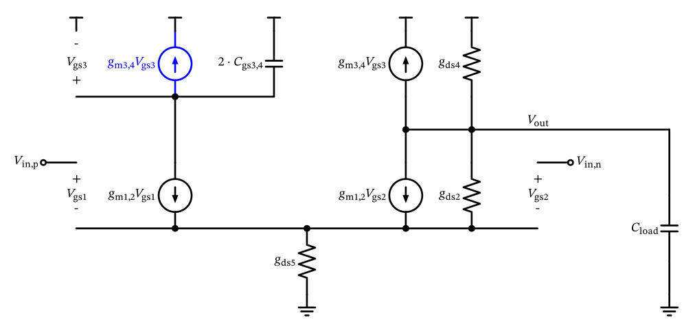
Figure 35: 5-transistor OTA open-loop small-signal model.
OTA Small-Signal Transfer Function
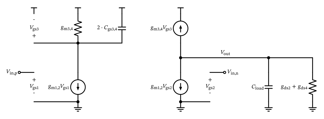
Figure 36: 5-transistor OTA small-signal model with further simplifications.
OTA Small-Signal Transfer Function
Realizing that \(V_\mathrm{gs1} = V_\mathrm{in,p} = V_\mathrm{in}/2\) and \(V_\mathrm{gs2} = V_\mathrm{in,n} = - V_\mathrm{in}/2\) we can formulate KCL at the output node to \[ -g_\mathrm{m3,4} V_\mathrm{gs3} - g_\mathrm{m1,2} \left( - \frac{V_\mathrm{in}}{2} \right) - V_\mathrm{out} (g_\mathrm{ds2} + g_\mathrm{ds4} + s C_\mathrm{load}) = 0. \tag{15}\]
\[ V_\mathrm{gs3} = -g_\mathrm{m1,2} \frac{V_\mathrm{in}}{2} \frac{1}{g_\mathrm{m3,4} + 2 \cdot s C_\mathrm{gs3,4}}. \tag{16}\]
OTA Small-Signal Transfer Function
\[ A(s) = \frac{V_\mathrm{out}(s)}{V_\mathrm{in}(s)} = \frac{g_\mathrm{m1,2}}{2} \frac{2 \cdot g_\mathrm{m3,4} + 2 \cdot s C_\mathrm{gs3,4}}{(g_\mathrm{m3,4} + 2 \cdot s C_\mathrm{gs3,4}) (g_\mathrm{ds2} + g_\mathrm{ds4} + s C_\mathrm{load})}. \tag{17}\]
\[ A(s \to 0) = A_0 = \frac{g_\mathrm{m1,2}}{g_\mathrm{ds2} + g_\mathrm{ds4}} \tag{18}\]
OTA Small-Signal Transfer Function
\[ A(s) \approx \frac{g_\mathrm{m1,2}}{2} \frac{2 g_\mathrm{m3,4}}{g_\mathrm{m3,4} \cdot s C_\mathrm{load}} = \frac{g_\mathrm{m1,2}}{s C_\mathrm{load}} \tag{19}\]
\[ f_\mathrm{ug} = \frac{g_\mathrm{m1,2}}{2 \pi C_\mathrm{load}} \tag{20}\]
OTA Small-Signal Transfer Function
Watch the Asymptote You Use
It is tempting to obtain \(f_\mathrm{ug}\) from the asymptote of Equation 17 for \(s \to \infty\), where both numerator and denominator are dominated by their \(s C_\mathrm{gs3,4}\) terms:
\[ A(s \to \infty) = \frac{g_\mathrm{m1,2}}{2 \cdot s C_\mathrm{load}} \tag{21}\]
OTA Small-Signal Transfer Function
Watch the Asymptote You Use
This differs from Equation 19 by a factor of two, and would predict a unity-gain frequency only half as large. The reason for the discrepancy is physical: Equation 21 describes the behavior above the doublet, where \(C_\mathrm{gs3,4}\) shorts out the current mirror so that the signal path through \(M_{3,4}\) is lost and only the direct path through \(M_2\) remains — hence half the transconductance. In a sensible design the doublet sits far above \(f_\mathrm{ug}\), so Equation 19 is the asymptote to use.
OTA Small-Signal Transfer Function
Looking at Equation 17, we see that we have a dominant pole at \(s_\mathrm{p}\) and a pole-zero doublet with \(s_\mathrm{pd}\)/\(s_\mathrm{zd}\): \[ s_\mathrm{p} = -\frac{g_\mathrm{ds2} + g_\mathrm{ds4}}{C_\mathrm{load}} \tag{22}\] \[ s_\mathrm{pd} = -\frac{g_\mathrm{m3,4}}{2 \cdot C_\mathrm{gs3,4}} \tag{23}\] \[ s_\mathrm{zd} = -\frac{g_\mathrm{m3,4}}{C_\mathrm{gs3,4}} \tag{24}\]
OTA Small-Signal Transfer Function
Why a Pole-Zero Doublet?
Looking at Equation 23 and Equation 24 we see that this pair is intimately linked by the same parameters and can only move together. Hence we call it a “doublet”. The effects of pole-zero doublets on the frequency response and settling time of OTAs can be found in (Kamath et al. 1974). This paper shows that doublets may cause severe degradation of settling time while only causing minor changes in the frequency response of the amplifier.
8.3.2 OTA Noise
OTA Noise
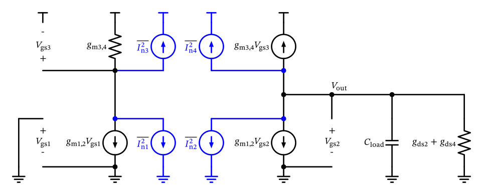
Figure 37: 5-transistor OTA small-signal model for noise calculation (added noise sources shown in blue).
OTA Noise
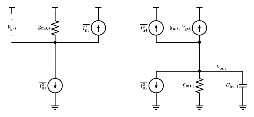
Figure 38: 5-transistor OTA simplified small-signal model for noise calculation.
OTA Noise
We see that \[ \overline{V_\mathrm{gs3}^2} = \frac{1}{g_\mathrm{m3,4}^2} \left( \overline{I_\mathrm{n1}^2} + \overline{I_\mathrm{n3}^2} \right). \]
OTA Noise
Noise Addition
Remember that uncorrelated noise quantities need to be power-summed (i.e., \(I^2 = I_1^2 + I_2^2\))!
OTA Noise
We can then sum the total output noise current \(\overline{I_\mathrm{n}}\) as \[ \overline{I_\mathrm{n}^2} = \overline{I_\mathrm{n2}^2} + \overline{I_\mathrm{n4}^2} + g_\mathrm{m3,4}^2 \frac{1}{g_\mathrm{m3,4}^2} \left( \overline{I_\mathrm{n1}^2} + \overline{I_\mathrm{n3}^2} \right) = 2 \left( \overline{I_\mathrm{n1,2}^2} + \overline{I_\mathrm{n3,4}^2} \right). \]
OTA Noise
\[ \begin{split} \overline{V_\mathrm{n,out}^2}(f) &= \frac{\overline{I_\mathrm{n}^2}}{\left| g_\mathrm{m1,2} + s C_\mathrm{load} \right|^{2}} = \frac{\overline{I_\mathrm{n}^2}}{g_\mathrm{m1,2}^2 + (2 \pi f C_\mathrm{load})^2} \\ &= \frac{8 k T (\gamma_{1,2} g_\mathrm{m1,2} + \gamma_{3,4} g_\mathrm{m3,4})}{g_\mathrm{m1,2}^2 + (2 \pi f C_\mathrm{load})^2}. \end{split} \]
OTA Noise
\[ V_\mathrm{n,out,rms}^2 = \int_0^\infty \overline{V_\mathrm{n,out}^2}(f) \cdot df = \frac{k T}{C_\mathrm{load}} \left( 2 \gamma_{1,2} + 2 \gamma_{3,4} \frac{g_\mathrm{m3,4}}{g_\mathrm{m1,2}} \right). \tag{25}\]
OTA Noise
Exercise: Derivation of 5T-OTA Performance
Please take your time and carefully go through the explanations and derivations for the 5-transistor-OTA in Section 8.2 and Section 8.3. Try to do the calculations yourself; if you get stuck, review the previous chapters. There are additional useful derivations in Section 18.
8.4 5T-OTA Sizing
5T-OTA Sizing
\[ V_\mathrm{ds,sat} = \frac{2}{g_\mathrm{m}/I_\mathrm{D}} \tag{26}\]
5T-OTA Sizing
Exercise: 5T-OTA Sizing
Please size the 5T-OTA according to the previous \(g_\mathrm{m}/I_\mathrm{D}\) and \(L\) suggestions. Please calculate the \(W\) of \(M_{1-6}\) and the total supply current. Please check whether gain error, total output noise, and turn-on settling are met with the calculated devices sizes and bias currents.
5T-OTA Sizing
Solution: 5T-OTA Sizing
Sizing for Basic 5T-OTA
Copyright 2024-2025 Harald Pretl
Licensed under the Apache License, Version 2.0 (the “License”); you may not use this file except in compliance with the License. You may obtain a copy of the License at http://www.apache.org/licenses/LICENSE-2.0
# define the given parameters as taken from the specification table or inital guesses
c_load = 50e-15
gm_id_m12 = 10
gm_id_m34 = 5
gm_id_m56 = 5
l_12 = 5
l_34 = 5
l_56 = 5
f_bw = 10e6 # -3dB bandwidth of the voltage buffer
i_total_limit = 10e-6
i_bias_in = 20e-6
output_voltage = 1.3
vin_min = 0.7
vin_max = 0.9
vdd_min = 1.45
vdd_max = 1.55
# we get the required gm of M1/2 from the -3dB bandwidth requirement of the voltage buffer specification
# note that the -3dB bandwidth of the voltage buffer with gain Av=1 is equal to the unity gain bandwidth
# of the ota, hence we set them equal here
# the unity-gain frequency of the 5T-OTA is f_ug = gm12 / (2*pi*C_load)
# on top of the bare specification we apply a design margin of:
# 3x for PVT variation plus the additional MOSFET parasitic loading
# 2x of reserve on dc gain and settling (the power budget allows for it)
bw_margin = 3 * 2
gm_m12 = bw_margin * 2*np.pi * f_bw * c_load
print('gm12 =', round(gm_m12/1e-3, 4), 'mS')gm12 = 0.0188 mS# since we know gm12 and the gmid we can calculate the bias current
id_m12 = gm_m12 / gm_id_m12
i_total = 2*id_m12
print('i_total (exact) =', round(i_total/1e-6, 1), 'µA')
# we round to 0.5µA bias currents
i_total = max(round(i_total / 1e-6 * 2) / 2 * 1e-6, 0.5e-6)
id_m12 = i_total/2
print('i_total (rounded) =', i_total/1e-6, 'µA')
if i_total < i_total_limit:
print('[info] power consumption target is met!')
else:
print('[info] power consumption target is NOT met!') i_total (exact) = 3.8 µA
i_total (rounded) = 4.0 µA
[info] power consumption target is met!# we calculate the dc gain
gm_gds_m12 = lv_nmos.lookup('GM_GDS', GM_ID=gm_id_m12, L=l_12, VDS=0.75, VSB=0)
gm_gds_m34 = lv_pmos.lookup('GM_GDS', GM_ID=gm_id_m34, L=l_34, VDS=0.75, VSB=0)
gds_m12 = gm_m12 / gm_gds_m12
gm_m34 = gm_id_m34 * i_total/2
gds_m34 = gm_m34 / gm_gds_m34
a0 = gm_m12 / (gds_m12 + gds_m34)
print('a0 =', round(20*np.log10(a0), 1), 'dB')a0 = 34.8 dB# we calculate the MOSFET capacitance which adds to Cload, to see the impact on the BW
gm_cgs_m12 = lv_nmos.lookup('GM_CGS', GM_ID=gm_id_m12, L=l_12, VDS=0.75, VSB=0)
gm_cdd_m12 = lv_nmos.lookup('GM_CDD', GM_ID=gm_id_m12, L=l_12, VDS=0.75, VSB=0)
gm_cdd_m34 = lv_pmos.lookup('GM_CDD', GM_ID=gm_id_m34, L=l_34, VDS=0.75, VSB=0)
c_load_parasitic = abs(gm_m12/gm_cgs_m12) + abs(gm_m12/gm_cdd_m12) + abs(gm_m34/gm_cdd_m34)
print('additional load capacitance =', round(c_load_parasitic/1e-15, 1), 'fF')
f_bw = gm_m12 / (2*np.pi * (c_load + c_load_parasitic))
print('unity gain bandwidth incl. parasitics =', round(f_bw/1e6, 2), 'MHz')additional load capacitance = 54.9 fF
unity gain bandwidth incl. parasitics = 28.59 MHz# we can now look up the VGS of the MOSFET
vgs_m12 = lv_nmos.look_upVGS(GM_ID=gm_id_m12, L=l_12, VDS=0.75, VSB=0.0)
vgs_m34 = lv_pmos.look_upVGS(GM_ID=gm_id_m34, L=l_34, VDS=0.75, VSB=0.0)
vgs_m56 = lv_nmos.look_upVGS(GM_ID=gm_id_m56, L=l_56, VDS=0.75, VSB=0.0)
print('vgs_12 =', round(float(vgs_m12), 3), 'V')
print('vgs_34 =', round(float(vgs_m34), 3), 'V')
print('vgs_56 =', round(float(vgs_m56), 3), 'V')vgs_12 = 0.367 V
vgs_34 = 0.729 V
vgs_56 = 0.591 Vslewing time = 0.034 µs
settling time = 0.028 µsvoltage gain error = -1.8 %# calculate total rms output noise
sth_m12 = lv_nmos.lookup('STH_GM', VGS=vgs_m12, L=l_12, VDS=0.75, VSB=0) * gm_m12
gamma_m12 = sth_m12/(4*1.38e-23*300*gm_m12)
sth_m34 = lv_pmos.lookup('STH_GM', VGS=vgs_m34, L=l_34, VDS=0.75, VSB=0) * gm_m34
gamma_m34 = sth_m34/(4*1.38e-23*300*gm_m34)
output_noise_rms = np.sqrt(1.38e-23*300 / (c_load + c_load_parasitic) * (2*gamma_m12 + 2*gamma_m34 * gm_m34/gm_m12))
print('output noise =', round(output_noise_rms/1e-6, 1), 'µVrms')output noise = 354.2 µVrms# calculate all widths
id_w_m12 = lv_nmos.lookup('ID_W', GM_ID=gm_id_m12, L=l_12, VDS=vgs_m12, VSB=0)
w_12 = id_m12 / id_w_m12
w_12_round = max(round(w_12*2)/2, 0.5)
print('M1/2 W =', round(w_12, 2), 'um, rounded W =', w_12_round, 'um')
id_m34 = id_m12
id_w_m34 = lv_pmos.lookup('ID_W', GM_ID=gm_id_m34, L=l_34, VDS=vgs_m34, VSB=0)
w_34 = id_m34 / id_w_m34
w_34_round = max(round(w_34*2)/2, 0.5)
print('M3/4 W =', round(w_34, 2), 'um, rounded W =', w_34_round, 'um')
id_w_m5 = lv_nmos.lookup('ID_W', GM_ID=gm_id_m56, L=l_56, VDS=vgs_m56, VSB=0)
w_5 = i_total / id_w_m5
w_5_round = max(round(w_5*2)/2, 0.5)
print('M5 W =', round(w_5, 2), 'um, rounded W =', w_5_round, 'um')
w_6 = w_5_round * i_bias_in / i_total
w_6_round = max(round(w_6*2)/2, 0.5)
print('M6 W =', round(w_6_round, 2), 'um')M1/2 W = 1.77 um, rounded W = 2.0 um
M3/4 W = 1.64 um, rounded W = 1.5 um
M5 W = 0.74 um, rounded W = 0.5 um
M6 W = 2.5 um# print out final design values
print('5T-OTA dimensioning:')
print('--------------------')
print('M1/2 W=', w_12_round, ', L=', l_12)
print('M3/4 W=', w_34_round, ', L=', l_34)
print('M5 W=', w_5_round, ', L=', l_56)
print('M6 W=', w_6_round, ', L=', l_56)
print()
print('5T-OTA performance summary:')
print('---------------------------')
print('supply current =', round(i_total/1e-6, 1), 'µA')
print('output noise =', round(output_noise_rms/1e-6, 1), 'µVrms')
print('voltage gain error =', round((gain_error-1)*100, 1), '%')
print('unity gain bandwidth incl. parasitics =', round(f_bw/1e6, 2), 'MHz')
print('turn-on time (slewing+settling) =', round((t_slew+t_settle)/1e-6, 3), 'µs')
print()
print('5T-OTA bias point check:')
print('------------------------')
print('headroom M1 =', round(vdd_min-vgs_m34+vgs_m12-vin_max, 3), 'V')
print('headroom M4 =', round(vdd_min-vin_max, 3), 'V')
print('headroom M5 =', round(vin_min-vgs_m12, 3), 'V')5T-OTA dimensioning:
--------------------
M1/2 W= 2.0 , L= 5
M3/4 W= 1.5 , L= 5
M5 W= 0.5 , L= 5
M6 W= 2.5 , L= 5
5T-OTA performance summary:
---------------------------
supply current = 4.0 µA
output noise = 354.2 µVrms
voltage gain error = -1.8 %
unity gain bandwidth incl. parasitics = 28.59 MHz
turn-on time (slewing+settling) = 0.062 µs
5T-OTA bias point check:
------------------------
headroom M1 = 0.188 V
headroom M4 = 0.55 V
headroom M5 = 0.333 V8.5 5T-OTA Simulation
5T-OTA Simulation
Exercise: 5T-OTA Design and Testbench
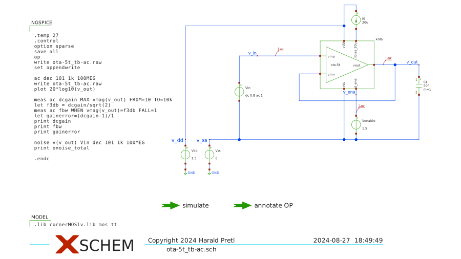
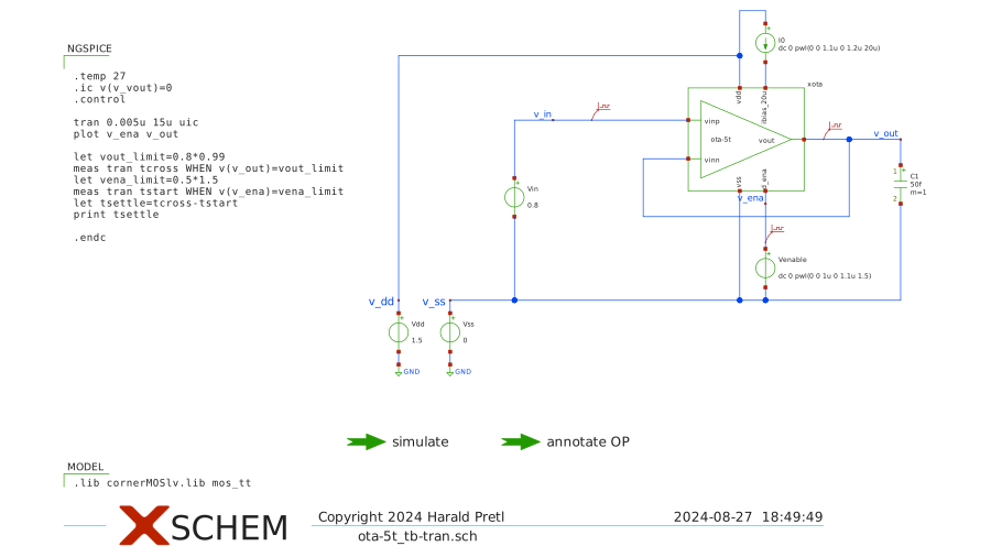
Please design the circuit of the 5T-OTA. Put the OTA circuit in a separate schematic, create a symbol for it, and use this symbol in a testbench you create in Xschem for this 5T-OTA used as a voltage buffer as shown in Figure 33. Use typical conditions for the simulation and check how well the specification in Table 2 is met and how well the derivations in Section 8.2 and Section 8.3 fit to the simulation results.
5T-OTA Simulation
Exercise: 5T-OTA Design and Testbench
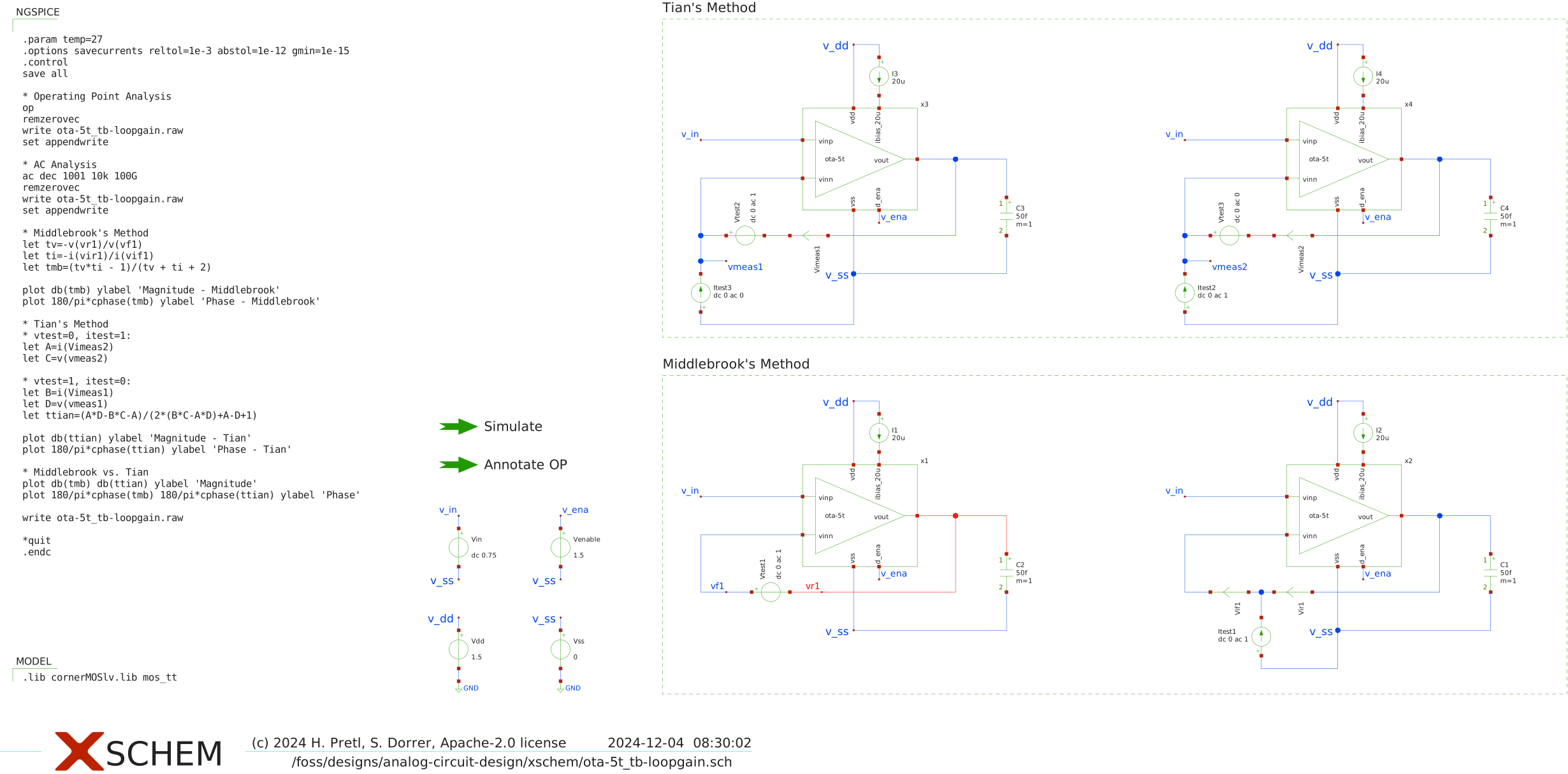
If you get stuck, you can find the testbench and 5T-OTA schematic here (for the small-signal analysis) and here (for the large-signal settling simulation). For interested students, the loop gain analysis with Middlebrook’s and Tian’s method of the 5T-OTA can be found here. A comprehensive technical white paper by Texas Instruments about operational amplifier stability theory and compensation methods can be found in (Kay and Wells 2025).
8.6 Component Mismatch
8.6.1 MOSFET Mismatch
- A variation of the threshold voltage (mainly due to variations in doping levels).
- A variation of the critical dimensions of the MOSFET (\(W\) and \(L\) as well as vertical dimensions).
MOSFET Mismatch
\[ \sigma\left\{\frac{\Delta I_\mathrm{D}}{I_\mathrm{D}}\right\} = \frac{A_\mathrm{mosfet}}{\sqrt{W L}} \tag{27}\]
MOSFET Mismatch
MOSFET Mismatch
Usually, the mismatch in MOSFETs is characterized via two mismatch parameters (Pelgrom et al. 1989):
- The threshold voltage mismatch standard deviation
\[ \sigma\left\{\Delta V_\mathrm{th}\right\} = \frac{A_\mathrm{vth}}{\sqrt{W L}} \tag{28}\]
- and standard deviation of the size mismatch
\[ \sigma\left\{\frac{\Delta (W/L)}{(W/L)}\right\} = \frac{A_\mathrm{k}}{\sqrt{W L}}. \tag{29}\]
The resulting standard deviation of the input offset voltage \(V_\mathrm{offs}\) of a differential pair with small \(g_\mathrm{m}/I_\mathrm{D}\) is then given by (Razavi 2017) \[ \sigma\left\{V_\mathrm{offs}\right\} = \sqrt{\left( \frac{V_\mathrm{GS}- V_\mathrm{th}}{2} \right)^2 \cdot \sigma^2\left\{\frac{\Delta (W/L)}{{(W/L)}}\right\} + \sigma^2\left\{\Delta V_\mathrm{th}\right\}}. \tag{30}\]
The mismatch in the drain current of two current-mirror transistors, characterized as the standard deviation and for small \(g_\mathrm{m}/I_\mathrm{D}\), is given by (Razavi 2017)
\[ \sigma^2\left\{\frac{\Delta I_\mathrm{D}}{I_\mathrm{D}}\right\} = \sigma^2\left\{\frac{\Delta (W/L)}{(W/L)}\right\} + 4 \cdot \sigma^2\left\{\frac{\Delta V_\mathrm{th}}{V_\mathrm{GS}- V_\mathrm{th}}\right\}. \tag{31}\]
MOSFET Mismatch
MOSFET Mismatch
To minimize the input offset voltage in a differential pair we should strive to minimize the overdrive voltage \(V_\mathrm{GS}- V_\mathrm{th}\) (i.e., to maximize \(g_\mathrm{m}/I_\mathrm{D}\), see Equation 30) and to minimize the mismatch in current mirrors we should target a large overdrive voltage (i.e., to minimize \(g_\mathrm{m}/I_\mathrm{D}\), see Equation 31). In both cases the MOSFET area \(W \cdot L\) needs to be large enough (see Equation 28 and Equation 29).
Mismatch: Design Rules
- Mismatch shrinks with gate area: \(\sigma\left\{\Delta V_\mathrm{th}\right\} = A_\mathrm{vth}/\sqrt{W L}\)
- Differential pair: small overdrive (high \(g_\mathrm{m}/I_\mathrm{D}\)) for low offset
- Current mirror: large overdrive (low \(g_\mathrm{m}/I_\mathrm{D}\)) for accurate currents
- Verify with Monte Carlo simulation (\(N \approx 250\) runs)
MOSFET Mismatch
Number of Monte Carlo Simulation Runs
The number of Monte Carlo simulation runs \(N\) has to be large enough to approach Gaussian distributions to allow estimation of the variances. However, this comes at the cost of a large simulation time, so a balance has to be found. Often, \(N = 250\) is a good compromise between simulation time and well-behaved parameter distributions.
8.6.2 Resistor Mismatch
\[ \sigma\left\{\frac{\Delta R}{R}\right\} = \frac{A_\mathrm{res}}{\sqrt{W L}} \tag{32}\]
Resistor Mismatch
- The current handling capability (the larger the \(W\), the more dc current a resistor can carry), and
- the resistor mismatch (the larger the \(W\), the larger the \(W L\) for a given \(L/W\)).
8.6.3 Capacitor Mismatch
\[ \sigma\left\{\frac{\Delta C}{C}\right\} = \frac{A_\mathrm{cap}}{\sqrt{W L}} \tag{33}\]
8.7 5T-OTA Simulation versus PVT and MC
5T-OTA Simulation versus PVT and MC
- The supply voltage of the circuit has tolerances, and thus we need to check the performance against this variation.
- The temperature at which the circuit is operated is likely changing. Also the performance against this has to be verified.
5T-OTA Simulation versus PVT and MC
- When manufacturing the wafers random variations in various process parameters lead to changed parameters of the integrated circuit components. In order to check for this effect, wafer foundries provide model files which shall cover these manufacturing excursions. Simplified, this leads to a slower or faster MOSFET, and usually NMOS and PMOS are not correlated, so we have the process corners SS, SF, TT, FS, and FF.
5T-OTA Simulation versus PVT and MC
- So far, we have only used the TT models in our simulations.
5T-OTA Simulation versus PVT and MC
- As an experienced designer you have a very solid understanding of the circuit, plus based on the analytic equations you can identify which combination of operating conditions will lead to a worst case performance. Thus, you can drastically reduce the number of corners to simulate, and you run them by hand.
- You are using a framework which highly automates this task of running a plethora of different simulations and evaluating the outcome. These frameworks are called simulation runners.
5T-OTA Simulation versus PVT and MC
Running CACE Simulation
The CACE simulation run can be started with
The simulation results are then placed into the cace/_docs folder. If in addition to the default Markdown report an HTML output is needed for easier review then using Pandoc it can be easily converted and viewed with with
5T-OTA Simulation versus PVT and MC
Note 2: CACE Summary for 5T-OTA
CACE Summary for ota-5t
netlist source: schematic
| Parameter | Tool | Result | Min Limit | Min Value | Typ Target | Typ Value | Max Limit | Max Value | Status |
|---|---|---|---|---|---|---|---|---|---|
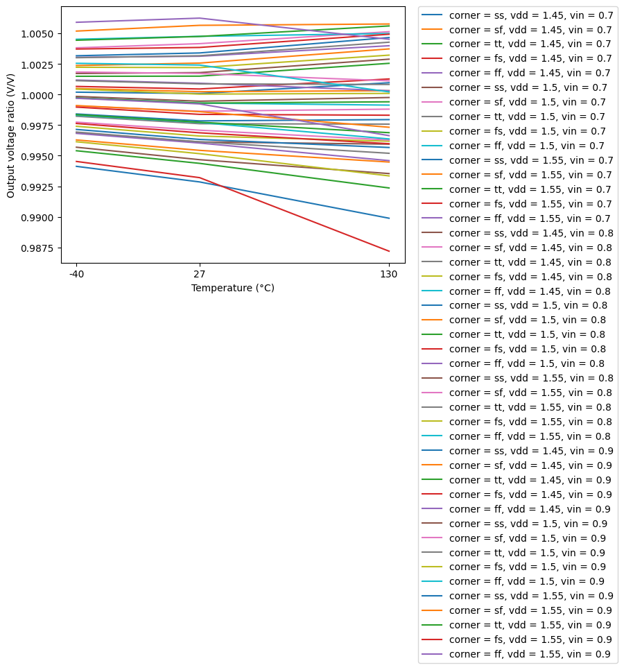
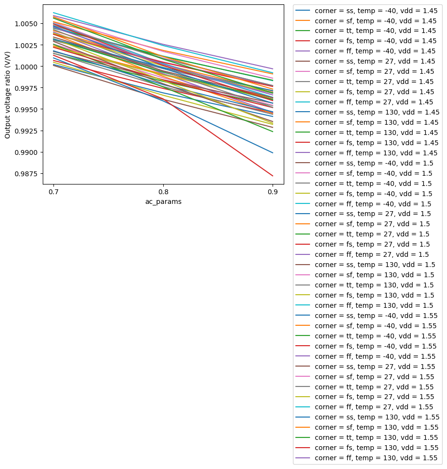
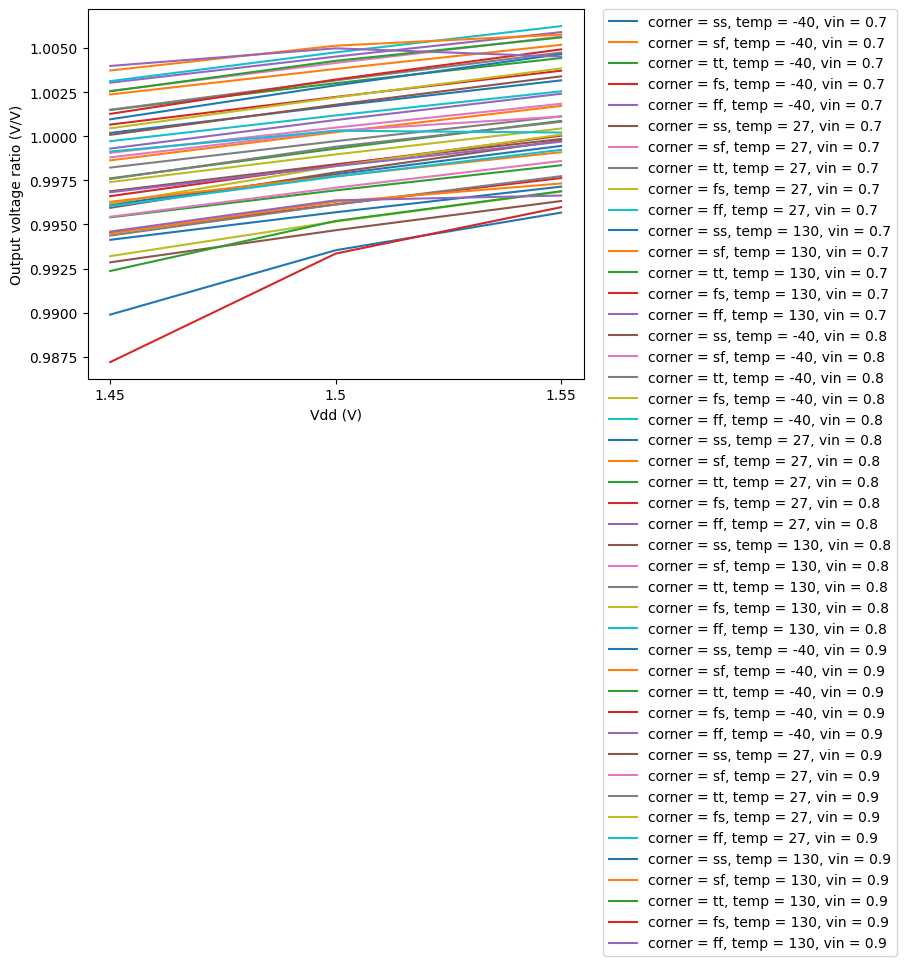
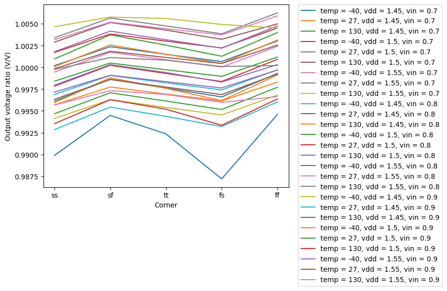
| Output voltage ratio | ngspice | gain | 0.97 V/V | 0.987 V/V | any | 1.000 V/V | 1.03 V/V | 1.007 V/V | Pass ✅ |
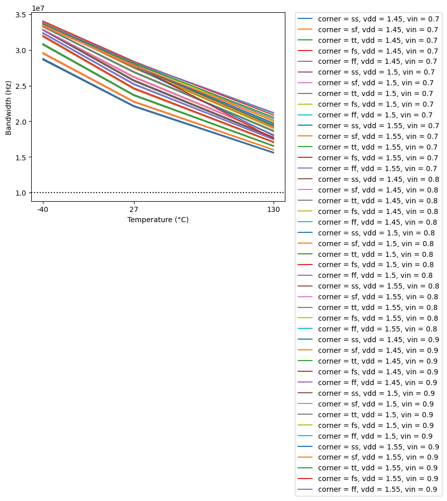
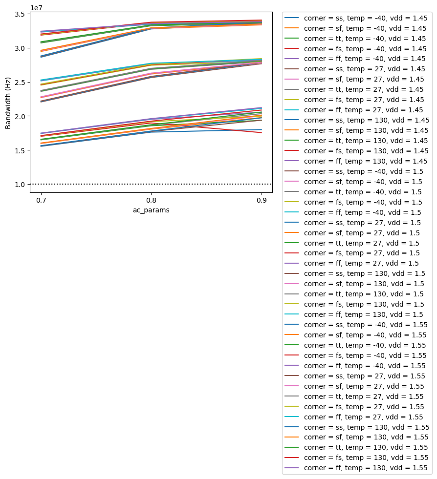
| Bandwidth | ngspice | bw | 10e6 Hz | 15550400.000 Hz | any | 26912100.000 Hz | any | 34052200.000 Hz | Pass ✅ |
| Output voltage ratio (MC) | ngspice | gain_mc | any | 0.994 V/V | any | 1.000 V/V | any | 1.005 V/V | Pass ✅ |
| Bandwidth (MC) | ngspice | bw_mc | 10e6 Hz | 26633900.000 Hz | any | 26917750.000 Hz | any | 27266300.000 Hz | Pass ✅ |
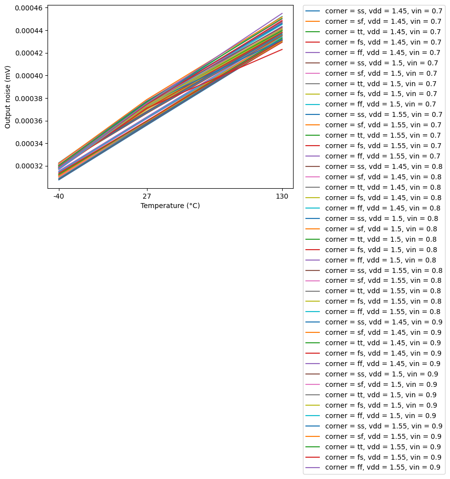
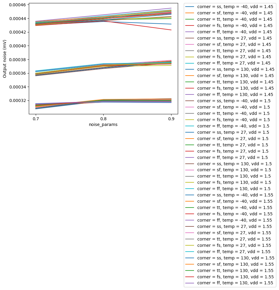
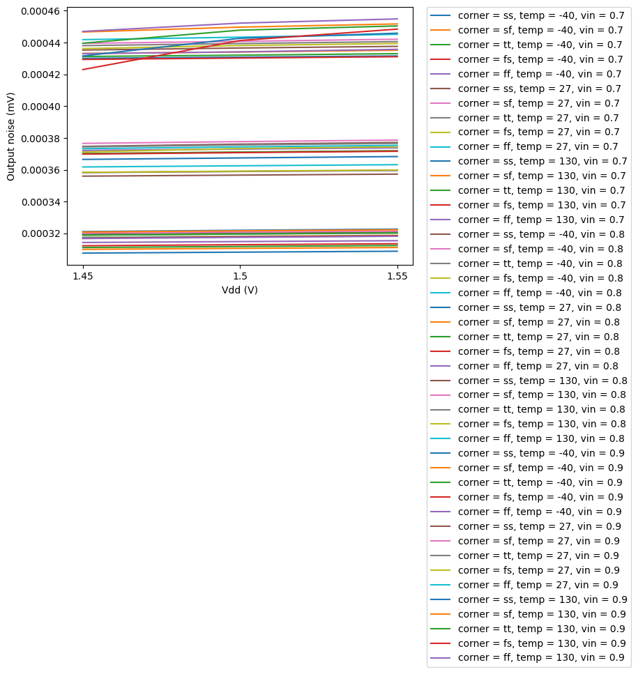
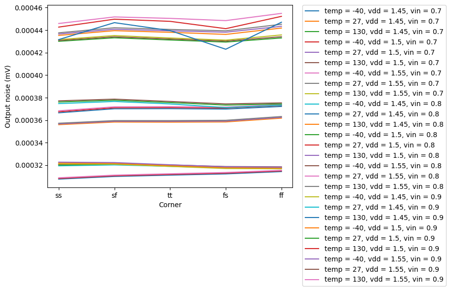
| Output noise | ngspice | noise | any | 0.308 mV | any | 0.371 mV | 1 mV | 0.454 mV | Pass ✅ |
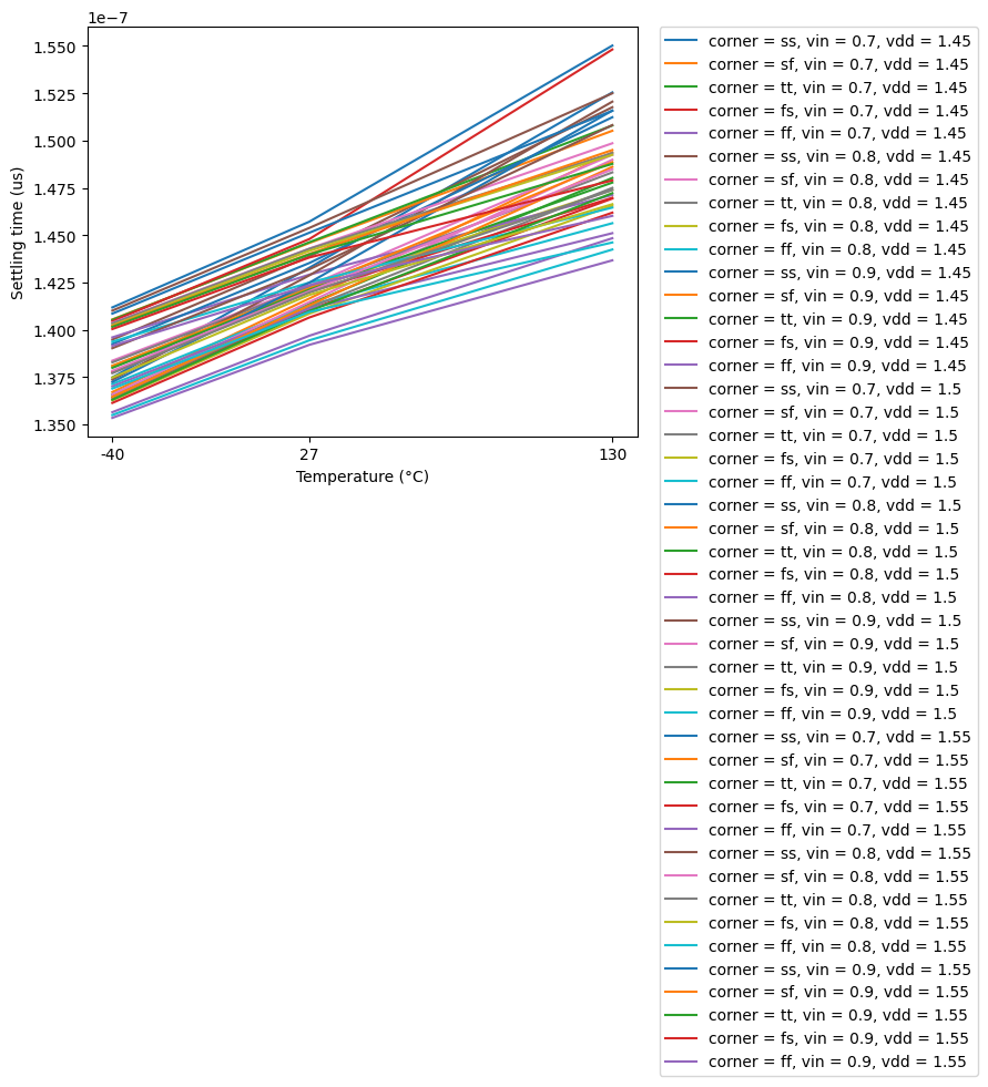
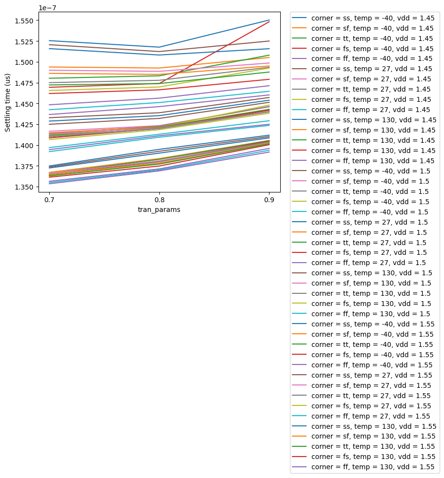
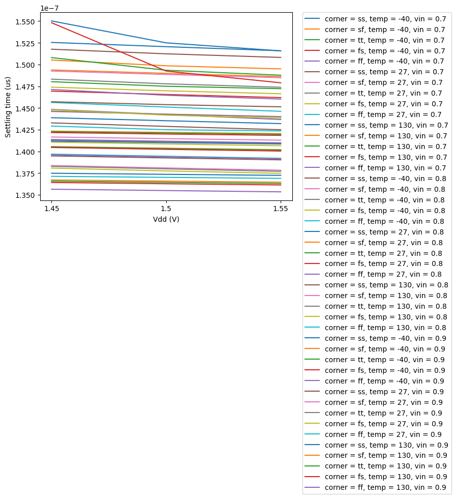
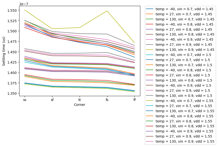
| Settling time | ngspice | tsettle | any | 0.137 us | any | 0.144 us | 10 us | 0.156 us | Pass ✅ |
Plots
gain_vs_temp
5T-OTA Simulation versus PVT and MC
CACE Summary for 5T-OTA
gain_vs_vin
5T-OTA Simulation versus PVT and MC
CACE Summary for 5T-OTA
gain_vs_vdd
5T-OTA Simulation versus PVT and MC
CACE Summary for 5T-OTA
gain_vs_corner
5T-OTA Simulation versus PVT and MC
CACE Summary for 5T-OTA
bw_vs_temp
5T-OTA Simulation versus PVT and MC
CACE Summary for 5T-OTA
bw_vs_vin
5T-OTA Simulation versus PVT and MC
CACE Summary for 5T-OTA
bw_vs_vdd
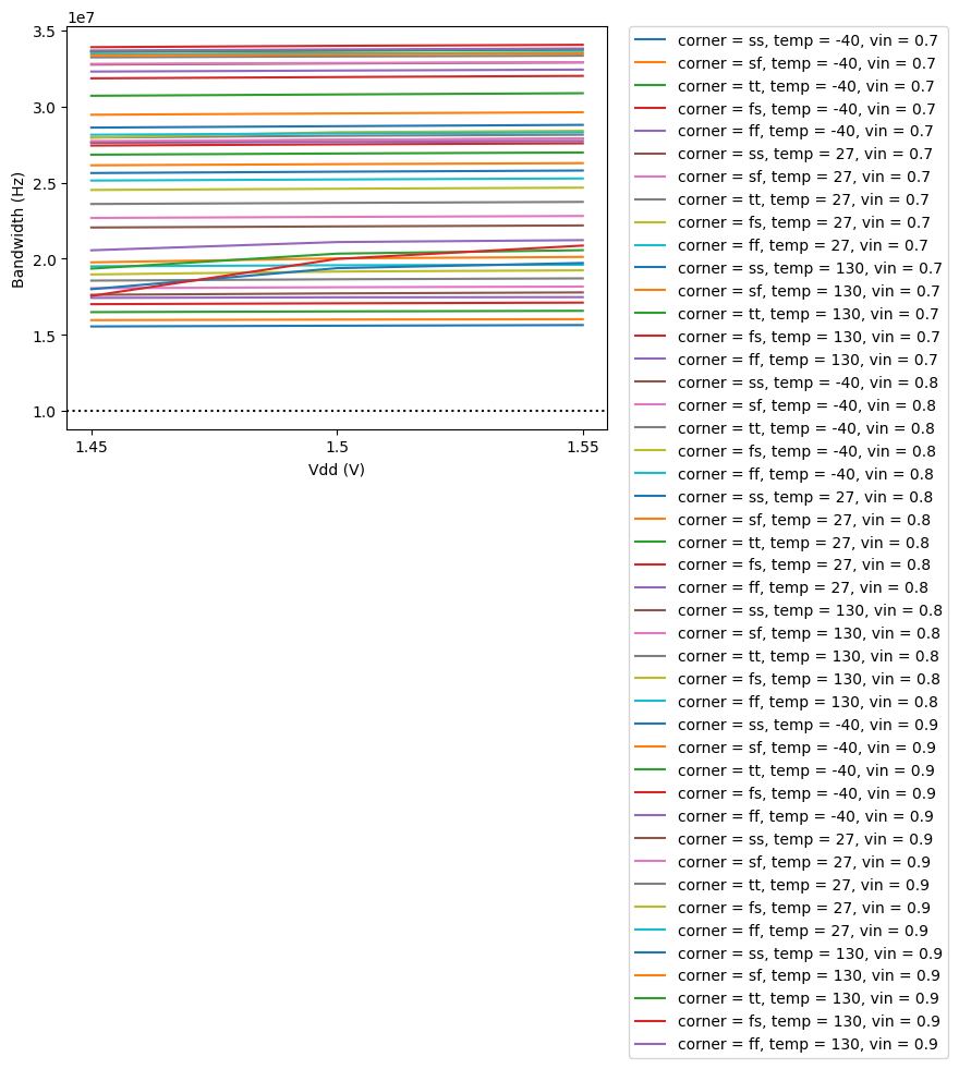
5T-OTA Simulation versus PVT and MC
CACE Summary for 5T-OTA
bw_vs_corner
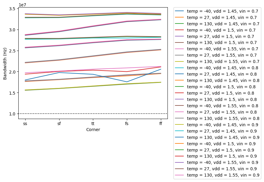
5T-OTA Simulation versus PVT and MC
CACE Summary for 5T-OTA
gain_mc
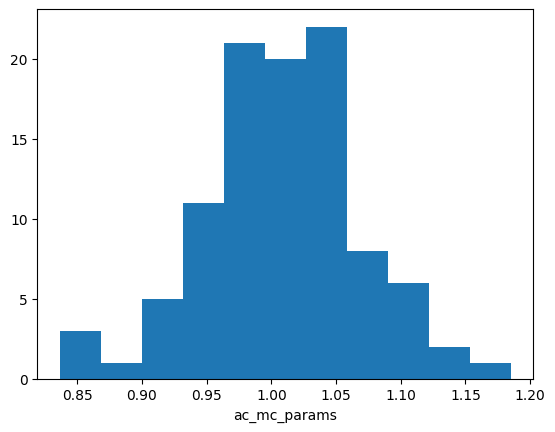
5T-OTA Simulation versus PVT and MC
CACE Summary for 5T-OTA
bw_mc
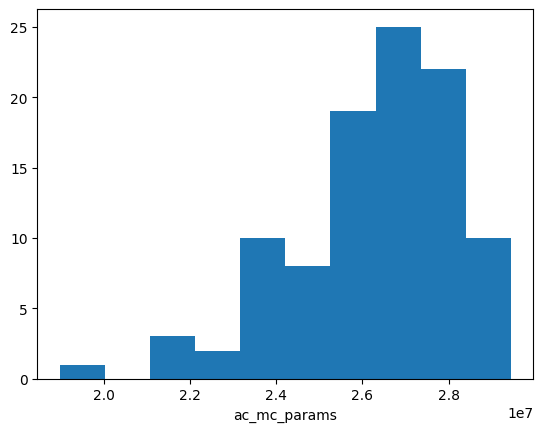
5T-OTA Simulation versus PVT and MC
CACE Summary for 5T-OTA
noise_vs_temp
5T-OTA Simulation versus PVT and MC
CACE Summary for 5T-OTA
noise_vs_vin
5T-OTA Simulation versus PVT and MC
CACE Summary for 5T-OTA
noise_vs_vdd
5T-OTA Simulation versus PVT and MC
CACE Summary for 5T-OTA
noise_vs_corner
5T-OTA Simulation versus PVT and MC
CACE Summary for 5T-OTA
settling_vs_temp
5T-OTA Simulation versus PVT and MC
CACE Summary for 5T-OTA
settling_vs_vin
5T-OTA Simulation versus PVT and MC
CACE Summary for 5T-OTA
settling_vs_vdd
5T-OTA Simulation versus PVT and MC
CACE Summary for 5T-OTA
settling_vs_corner
8.7.1 PVT Simulation Analysis
8.7.2 Monte Carlo Simulation Analysis
Monte Carlo Simulation Analysis
Exercise: Mismatch Sensitivity of the 5T-OTA
Go back to Section 8.4 and repeat the sizing procedure of the 5T-OTA with a significantly shorter \(L\) of the differential pair \(M_{1,2}\) and the current mirror \(M_{3,4}\), while keeping the \(g_\mathrm{m}/I_\mathrm{D}\) values. Estimate the expected input offset voltage with Equation 30 and Equation 31 first.
Monte Carlo Simulation Analysis
Exercise: Mismatch Sensitivity of the 5T-OTA
Then, update the transistor sizes in the 5T-OTA schematic and repeat the CACE simulations (PVT and Monte Carlo). How does the spread of the output voltage ratio compare to your estimate? How short can \(L\) become before the output voltage specification is violated, and what happens to the other performance parameters?
8.8 OTA Variants
OTA Variants
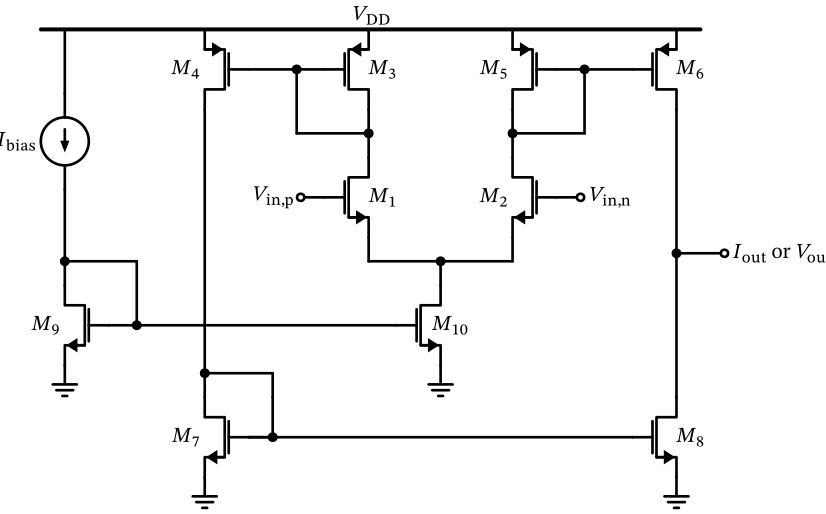
Figure 39: Single-ended OTA with rail-to-rail output stage.
OTA Variants
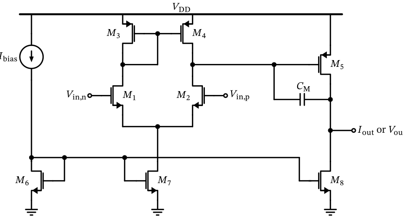
Figure 40: Single-ended two-stage OTA with rail-to-rail output.
OTA Variants
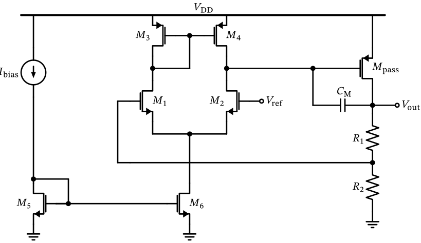
Figure 41: A basic low-dropout voltage regulator (LDO) with Miller compensation.
OTA Variants
\[ V_\mathrm{out} \approx V_\mathrm{ref} \left( 1 + \frac{R_1}{R_2} \right) \]
References
Baker, R. J. n.d. “Bad Circuit Design 3 - Compensating an Op-Amp.” https://cmosedu.com/cmos1/bad_design/bad_design3/bad_design_3.htm.
Gray, Paul R., Paul J. Hurst, Stephen H. Lewis, and Robert G. Meyer. 2009. Analysis and Design of Analog Integrated Circuits. Wiley.
Kamath, B. Y. T., R. G. Meyer, and P. R. Gray. 1974. “Relationship Between Frequency Response and Settling Time of Operational Amplifiers.” IEEE Journal of Solid-State Circuits 9 (6): 347–52. https://doi.org/10.1109/JSSC.1974.1050527.
Kay, A., and C. Wells. 2025. “Technical White Paper - Operational Amplifier Stability Theory and Compensation Methods.” Texas Instruments. https://www.ti.com/lit/wp/sboa626/sboa626.pdf.
Murmann, Boris. 2013. Analysis and Design of Elementary MOS Amplifier Stages. NTS Press.
Pelgrom, M. J. M., A. C. J. Duinmaijer, and A. P. G. Welbers. 1989. “Matching Properties of MOS Transistors.” IEEE Journal of Solid-State Circuits 24 (5): 1433–39. https://doi.org/10.1109/JSSC.1989.572629.
Razavi, Behzad. 2017. Design of Analog CMOS Integrated Circuits. McGraw-Hill.
Razavi, Behzad. 2019. “The Low Dropout Regulator [A Circuit for All Seasons].” IEEE Solid-State Circuits Magazine 11 (2): 8–13. https://doi.org/10.1109/mssc.2019.2910952.