Improved (Telescopic) OTA

Analog (Integrated) Circuit Design

11 Improved (Telescopic) OTA

Improved (Telescopic) OTA

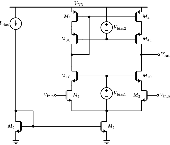
Figure 58: The improved OTA based on the 5T-OTA design.

Improved (Telescopic) OTA

Cascode Bias Voltage Generation

It is critically important for stable performance across PVT that the bias voltages for the cascode gates are created in a manner that tracks variations with process, temperature, and supply voltage!

Improved (Telescopic) OTA

Exercise: Cascode Current Mirror vs. High-Swing Cascode Current Mirror

Try to verify the above statement of equal drain-source voltages by deriving both, an equation for \(V_\mathrm{DS4}\) assuming a high-swing cascode current mirror (Figure 58) and \(V_\mathrm{DS4}\) in case of a simple cascode current mirror, where the reference branch \((M_\mathrm{3,3C})\) is comprised of two MOSFET diodes.

Improved (Telescopic) OTA

A simplified small-signal gain calculation of this improved OTA uses the result of Equation 18 and Equation 35 to arrive at the approximate dc gain of \[ A_0 \approx \frac{g_\mathrm{m12}}{g_\mathrm{ds2} \frac{g_\mathrm{ds2C}}{g_\mathrm{m2C}} + g_\mathrm{ds4} \frac{g_\mathrm{ds4C}}{g_\mathrm{m4C}}} \tag{45}\] leading to a significant boost in dc gain due to cascoding.

Improved (Telescopic) OTA

  1. save area (a smaller \(L\) will lead to a smaller \(W\) for a given \(W/L\) ratio) and
  2. push the additional poles and zeros at the inner nodes of the cascode transistors (e.g., the connection of the drain of \(M_4\) to the source of \(M_\mathrm{4C}\)) to higher frequencies to result in stable behavior and a reasonable gain transfer function (too many poles and zeros in the pass band of the amplifier create many issues with stability margin).

11.1 Sizing the Improved OTA

Sizing the Improved OTA

Improved OTA Sizing

Sizing for Basic (Improved) OTA

Copyright 2024-2025 Harald Pretl

Licensed under the Apache License, Version 2.0 (the “License”); you may not use this file except in compliance with the License. You may obtain a copy of the License at http://www.apache.org/licenses/LICENSE-2.0

# read table data
from pygmid import Lookup as lk
import numpy as np
lv_nmos = lk('sg13_lv_nmos.mat')
lv_pmos = lk('sg13_lv_pmos.mat')
# list of parameters: VGS, VDS, VSB, L, W, NFING, ID, VT, GM, GMB, GDS, CGG, CGB, CGD, CGS, CDD, CSS, STH, SFL
# if not specified, minimum L, VDS=max(vgs)/2=0.9 and VSB=0 are used 
# define the given parameters as taken from the specification table or initial guesses
c_load = 50e-15
gm_id_m12 = 13
gm_id_m12c = 13
gm_id_m34 = 13
gm_id_m34c = 13
gm_id_m56 = 13
l_12 = 0.5
l_12c = 0.5
l_34 = 0.5
l_34c = 0.5
l_56 = 5
f_bw = 10e6 # -3dB bandwidth of the voltage buffer
i_total_limit = 10e-6 # we plan 2x5uA in addition for additional bias voltage generation
i_bias_in = 5e-6
output_voltage = 1.3
vin_min = 0.7
vin_max = 0.9
vdd_min = 1.45
vdd_max = 1.55
vds_headroom = 0.2
# we get the required gm of M1/2 from the -3dB bandwidth requirement of the voltage buffer specification
# note that the -3dB bandwidth of the voltage buffer with gain Av=1 is equal to the unity gain bandwidth
# of the ota, hence we set them equal here
# the unity-gain frequency of the OTA is f_ug = gm12 / (2*pi*C_load)
# on top of the bare specification we apply a design margin of:
#   3x for PVT variation plus the additional MOSFET parasitic loading
#   3x to buy more dc gain (there is still power left in the budget)
#   2x of reserve on settling
bw_margin = 3 * 3 * 2
gm_m12 = bw_margin * 2*np.pi * f_bw * c_load
print('gm12 =', round(gm_m12/1e-3, 4), 'mS')
gm12 = 0.0565 mS
# since we know gm12 and the gmid we can calculate the bias current
id_m12 = gm_m12 / gm_id_m12
i_total = 2*id_m12
print('i_total (exact) =', round(i_total/1e-6, 1), 'µA')
# we round to 0.5µA bias currents
i_total = max(round(i_total / 1e-6 * 2) / 2 * 1e-6, 0.5e-6)
# here is a manual override to set the current; we keep a reserve of 2µA for bias branch
i_total = 8e-6
id_m12 = i_total/2

print('i_total (rounded) =', i_total/1e-6, 'µA')
if i_total < i_total_limit:
    print('[info] power consumption target is met!')
else:
    print('[info] power consumption target is NOT met!') 
i_total (exact) = 8.7 µA
i_total (rounded) = 8.0 µA
[info] power consumption target is met!
# we calculate the dc gain
gm_gds_m12 = lv_nmos.lookup('GM_GDS', GM_ID=gm_id_m12, L=l_12, VDS=vds_headroom, VSB=2*vds_headroom)
gm_gds_m12c = lv_nmos.lookup('GM_GDS', GM_ID=gm_id_m12c, L=l_12c, VDS=vds_headroom, VSB=3*vds_headroom)
gm_gds_m34 = lv_pmos.lookup('GM_GDS', GM_ID=gm_id_m34, L=l_34, VDS=vds_headroom, VSB=0)
gm_gds_m34c = lv_pmos.lookup('GM_GDS', GM_ID=gm_id_m34c, L=l_34c, VDS=vds_headroom, VSB=vds_headroom)
# conductance of lower cascoded differential pair
gds_m12 = gm_m12 / gm_gds_m12
gds_m12_casc = gds_m12 / gm_gds_m12c
# conductance of upper cascoded current mirror
gm_m34 = gm_id_m34 * i_total/2
gds_m34 = gm_m34 / gm_gds_m34
gds_m34_casc = gds_m34 / gm_gds_m34c

print('gds_12 =', round(gds_m12/1e-6, 3), 'µs')
print('gm_12c/gds_12c =',round(float(gm_gds_m12c), 1))
print('gds_34 =', round(gds_m34/1e-6, 3), 'µs')
print('gm_34c/gds_34c =', round(float(gm_gds_m34c), 1))

a0 = gm_m12 / (gds_m12_casc + gds_m34_casc)
print('a0 =', round(20*np.log10(a0), 1), 'dB')
gds_12 = 4.026 µs
gm_12c/gds_12c = 13.4
gds_34 = 2.031 µs
gm_34c/gds_34c = 24.9
a0 = 43.4 dB
# we calculate the MOSFET capacitance which adds to Cload, to see the impact on the BW
gm_cgs_m12 = lv_nmos.lookup('GM_CGS', GM_ID=gm_id_m12, L=l_12, VDS=vds_headroom, VSB=2*vds_headroom)
gm_cdd_m12c = lv_nmos.lookup('GM_CDD', GM_ID=gm_id_m12c, L=l_12c, VDS=vds_headroom, VSB=3*vds_headroom)
gm_cdd_m34c = lv_pmos.lookup('GM_CDD', GM_ID=gm_id_m34c, L=l_34c, VDS=vds_headroom, VSB=vds_headroom)

c_load_parasitic = abs(gm_m12/gm_cgs_m12) + abs(gm_m12/gm_cdd_m12c) + abs(gm_m34/gm_cdd_m34c)
print('additional load capacitance =', round(c_load_parasitic/1e-15, 1), 'fF')

f_bw = gm_m12 / (2*np.pi * (c_load + c_load_parasitic))
print('unity gain bandwidth incl. parasitics =', round(f_bw/1e6, 2), 'MHz')
additional load capacitance = 5.5 fF
unity gain bandwidth incl. parasitics = 81.15 MHz
# we can now look up the VGS of the MOSFET
vgs_m12 = lv_nmos.look_upVGS(GM_ID=gm_id_m12, L=l_12, VDS=vds_headroom, VSB=2*vds_headroom)
vgs_m12c = lv_nmos.look_upVGS(GM_ID=gm_id_m12c, L=l_12c, VDS=vds_headroom, VSB=3*vds_headroom)
vgs_m34 = lv_pmos.look_upVGS(GM_ID=gm_id_m34, L=l_34, VDS=vds_headroom, VSB=0.0) 
vgs_m34c = lv_pmos.look_upVGS(GM_ID=gm_id_m34c, L=l_34c, VDS=vds_headroom, VSB=vds_headroom) 
vgs_m56 = lv_nmos.look_upVGS(GM_ID=gm_id_m56, L=l_56, VDS=vds_headroom, VSB=0.0) 

print('vgs_12  =', round(float(vgs_m12), 3), 'V')
print('vgs_12c =', round(float(vgs_m12c), 3), 'V')
print('vgs_34  =', round(float(vgs_m34), 3), 'V')
print('vgs_34c =', round(float(vgs_m34c), 3), 'V')
print('vgs_56  =', round(float(vgs_m56), 3), 'V')
vgs_12  = 0.436 V
vgs_12c = 0.458 V
vgs_34  = 0.475 V
vgs_34c = 0.512 V
vgs_56  = 0.318 V
# calculate settling time due to slewing with the calculated bias current
t_slew = (c_load + c_load_parasitic) * output_voltage / i_total
print('slewing time  =', round(t_slew/1e-6, 3), 'µs')
t_settle = 5/(2*np.pi*f_bw)
print('settling time =', round(t_settle/1e-6, 3), 'µs')
slewing time  = 0.009 µs
settling time = 0.01 µs
# calculate voltage gain error
gain_error = a0 / (1 + a0)
print('voltage gain error =', round((gain_error-1)*100, 1), '%')
voltage gain error = -0.7 %
# calculate total rms output noise
sth_m12 = lv_nmos.lookup('STH_GM', VGS=vgs_m12, L=l_12, VDS=vds_headroom, VSB=2*vds_headroom) * gm_m12
gamma_m12 = sth_m12/(4*1.38e-23*300*gm_m12)

sth_m34 = lv_pmos.lookup('STH_GM', VGS=vgs_m34, L=l_34, VDS=vds_headroom, VSB=0) * gm_m34
gamma_m34 = sth_m34/(4*1.38e-23*300*gm_m34)

output_noise_rms = np.sqrt(1.38e-23*300 / (c_load + c_load_parasitic) * (2*gamma_m12 + 2*gamma_m34 * gm_m34/gm_m12))
print('output noise =', round(output_noise_rms/1e-6, 1), 'µVrms')
output noise = 555.4 µVrms
# calculate all widths
id_w_m12 = lv_nmos.lookup('ID_W', GM_ID=gm_id_m12, L=l_12, VDS=vds_headroom, VSB=2*vds_headroom)
w_12 = id_m12 / id_w_m12
w_12_round = max(round(w_12*2)/2, 0.5)
print('M1/2  W =', round(w_12, 2), 'um, rounded W =', w_12_round, 'um')

id_m12c = id_m12
id_w_m12c = lv_nmos.lookup('ID_W', GM_ID=gm_id_m12c, L=l_12c, VDS=vds_headroom, VSB=3*vds_headroom)
w_12c = id_m12c / id_w_m12c
w_12c_round = max(round(w_12c*2)/2, 0.5)
print('M1/2c W =', round(w_12c, 2), 'um, rounded W =', w_12c_round, 'um')

id_m34 = id_m12
id_w_m34 = lv_pmos.lookup('ID_W', GM_ID=gm_id_m34, L=l_34, VDS=vds_headroom, VSB=0)
w_34 = id_m34 / id_w_m34
w_34_round = max(round(w_34*2)/2, 0.5) 
print('M3/4  W =', round(w_34, 2), 'um, rounded W =', w_34_round, 'um')

id_m34c = id_m12
id_w_m34c = lv_pmos.lookup('ID_W', GM_ID=gm_id_m34c, L=l_34c, VDS=vds_headroom, VSB=vds_headroom)
w_34c = id_m34c / id_w_m34c
w_34c_round = max(round(w_34c*2)/2, 0.5) 
print('M3/4c W =', round(w_34c, 2), 'um, rounded W =', w_34c_round, 'um')

id_w_m5 = lv_nmos.lookup('ID_W', GM_ID=gm_id_m56, L=l_56, VDS=vds_headroom, VSB=0)
w_5 = i_total / id_w_m5
w_5_round = max(round(w_5*2)/2, 0.5)
print('M5    W =', round(w_5, 2), 'um, rounded W =', w_5_round, 'um')

w_6 = w_5_round * i_bias_in / i_total
print('M6    W =', round(w_6, 2), 'um')
M1/2  W = 0.83 um, rounded W = 1.0 um
M1/2c W = 0.8 um, rounded W = 1.0 um
M3/4  W = 3.28 um, rounded W = 3.5 um
M3/4c W = 2.99 um, rounded W = 3.0 um
M5    W = 14.2 um, rounded W = 14.0 um
M6    W = 8.75 um
# Print out final design values
print('Improved OTA dimensioning:')
print('--------------------------')
print('M1/2  W=', w_12_round, ', L=', l_12)
print('M1/2c W=', w_12c_round, ', L=', l_12c)
print('M3/4  W=', w_34_round, ', L=', l_34)
print('M3/4c W=', w_34c_round, ', L=', l_34c)
print('M5   W=', w_5_round, ', L=', l_56)
print('M6   W=', round(w_6, 2), ', L=', l_56)
print()
print('Improved OTA performance summary:')
print('---------------------------------')
print('supply current =', round(i_total/1e-6, 1), 'µA')
print('output noise =', round(output_noise_rms/1e-6, 1), 'µVrms')
print('voltage gain error =', round((gain_error-1)*100, 1), '%')
print('unity gain bandwidth incl. parasitics =', round(f_bw/1e6, 2), 'MHz')
print('turn-on time (slewing+settling) =', round((t_slew+t_settle)/1e-6, 3), 'µs')
print()
print('Improved OTA bias point check:')
print('------------------------------')
print('headroom M1+M1c =', round(vdd_min-vgs_m34+vgs_m12-vin_max, 3), 'V')
print('headroom M4+M4c =', round(vdd_min-vin_max, 3), 'V')
print('headroom M5     =', round(vin_min-vgs_m12, 3), 'V')
Improved OTA dimensioning:
--------------------------
M1/2  W= 1.0 , L= 0.5
M1/2c W= 1.0 , L= 0.5
M3/4  W= 3.5 , L= 0.5
M3/4c W= 3.0 , L= 0.5
M5   W= 14.0 , L= 5
M6   W= 8.75 , L= 5

Improved OTA performance summary:
---------------------------------
supply current = 8.0 µA
output noise = 555.4 µVrms
voltage gain error = -0.7 %
unity gain bandwidth incl. parasitics = 81.15 MHz
turn-on time (slewing+settling) = 0.019 µs

Improved OTA bias point check:
------------------------------
headroom M1+M1c = 0.512 V
headroom M4+M4c = 0.55 V
headroom M5     = 0.264 V

Sizing the Improved OTA

Exercise: Improved OTA Sizing

Please take a detailed look at the above sizing notebook and play with the numbers and calculations. Do you find a better trade-off for the input parameters? Can you understand the thinking process behind the choices and calculations?

11.2 Designing the Improved OTA

Designing the Improved OTA

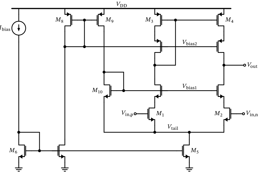
Figure 59: The improved OTA based on the 5T-OTA design with biasing details shown.

Designing the Improved OTA
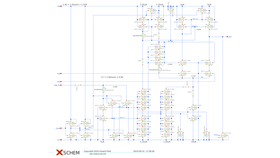
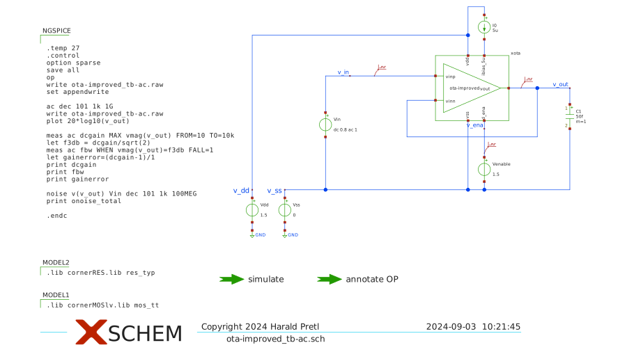
Figure 60: Improved OTA design in Xschem.

11.2.1 Discussion of the OTA Design

  1. For easier navigation, the device identifiers are consistent with the circuit sketch in Figure 58.

Discussion of the OTA Design

  1. Some MOSFET dimensions are rounded to make a better fit in the IC layout. Please also look carefully at \(W\), \(L\), and \(\mathrm{ng}\). The parameter \(\mathrm{ng}\) defines how the total \(W\) of a MOSFET should be split into individual MOSFET fingers with \(W_\mathrm{f} = W / \mathrm{ng}\). This is done to arrive at a suitably sized MOSFET physical implementation. As we will not deal with IC layout in this lecture we will leave it at that.

Discussion of the OTA Design

  1. In order to allow good matching in the IC layout, MOSFETs (and other components) have to be constructed from equal pieces. To that end, \(W/L\) scaling is done using unit elements (see finger width \(W_\mathrm{f}\)). Sometimes, besides \(W\) the length \(L\) has to be scaled, and this leads to the odd-looking series stacking of some MOSFETs (easily recognizable by the connected gates).

Discussion of the OTA Design

  1. In order to increase circuit readability, a subcircuit could be constructed hiding this series stacking of MOSFET, but it is sometimes easier to avoid subcircuits. There is a fine line in this trade-off, sometimes a depth of 4 is the decision point between subcircuit use/no-use.

Discussion of the OTA Design

  1. As you can (hopefully) see the circuit is carefully drawn to ease readability. Important nets are named, text comments state certain properties like nominal voltage levels, bias currents, etc. Current sensing elements are added to directly see the dc currents in the circuit simulation.

Discussion of the OTA Design

  1. The bias voltage generation for the cascodes is included as well. The voltage drop for the bottom transistors is developed by properly scaling the MOSFETs in the reference branch. We reduce the \(W/L\) ratio to increase the \(V_\mathrm{GS}\) to create a voltage headroom for the bottom MOSFET. We are using a dummy branch for bias generation (constructed with \(M_\mathrm{7-10}\)).

Discussion of the OTA Design

  1. The floating bias voltage \(V_\mathrm{bias1}\) is created by implementing a current source from \(V_\mathrm{DD}\) (\(M_\mathrm{9}\)), then a MOSFET diode \(M_{10}\), and an increased current towards \(V_\mathrm{SS}\) through \(M_\mathrm{5}\).

Discussion of the OTA Design

  1. Power-down transistors \(M_{\mathrm{pd,}x}\) are added to allow a proper shutdown of the circuit with a digital enable input. It is generally a good idea to clamp floating nodes in off-mode so that no issues during power-down (like increased leakage currents) or delayed startup or shutdown are occurring. It is further a good design principle to buffer all incoming digital signals with inverters (\(M_\mathrm{pd,1-4}\)) connected to the local supply.

Discussion of the OTA Design

  1. This lowers the risk of unwanted noise coupling or excessive slew rates on the incoming digital signals.
  2. Sensitive bias nodes are buffered with decoupling capacitors. We are using MOSFETs as nonlinear capacitors, which is not an issue in this application, but we value the increased capacitive density. Please note how the MOSFET are connected (some are tied to \(V_\mathrm{DD}\) while others are tied to \(V_\mathrm{SS}\)).

Discussion of the OTA Design

Parallel Connection

Note that a parallel connection of devices is effectively possible using the multiplier notation of Xschem.

11.3 Simulation of Improved OTA

Simulation of Improved OTA

Figure 61: Simulation testbench of the improved OTA design (small-signal).

Simulation of Improved OTA
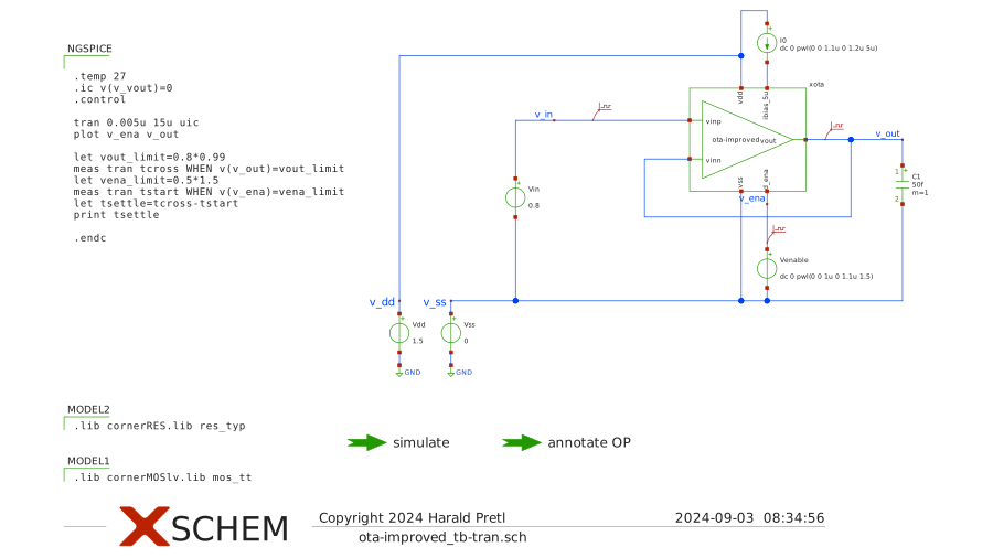
Figure 62: Simulation testbench of the improved OTA design (large-signal).

Simulation of Improved OTA
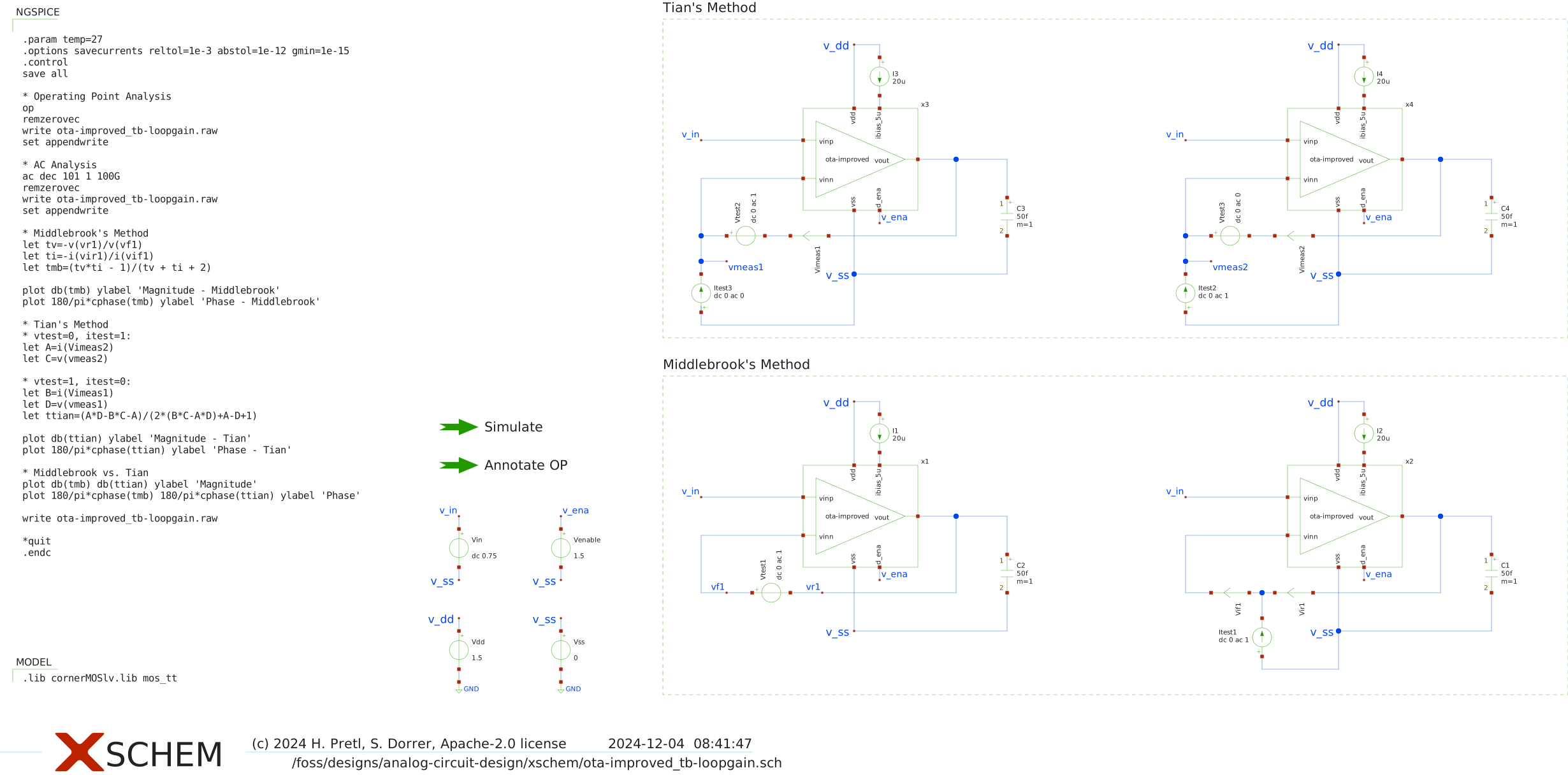
Figure 63: Simulation testbench of the improved OTA design (loop gain analysis).

Simulation of Improved OTA

Exercise: Improved OTA Initial Simulation

Please use the above testbenches to simulate the improved OTA:

  1. Check the dc bias points. Are they good? How stable are they across PVT variations?
  2. What are the small-signal parameters like gain, noise and bandwidth? Are they fitting the specification?
  3. What is large-signal performance? Is the settling fast enough? Is the settling well behaved, i.e., are there overshoots or other strange ringing indicating potential stability issues?

Simulation of Improved OTA

Exercise: Improved OTA Initial Simulation

  1. Try to improve the design. Change various device parameters and see what happens. Whenever you change something, check the dc operating point first. If the dc operating point is not good no further simulations make sense.

11.4 Corner Simulation of Improved OTA

Corner Simulation of Improved OTA

Note 3: CACE Summary for Improved OTA

CACE Summary for ota-improved

netlist source: schematic

Parameter Tool Result Min Limit Min Value Typ Target Typ Value Max Limit Max Value Status
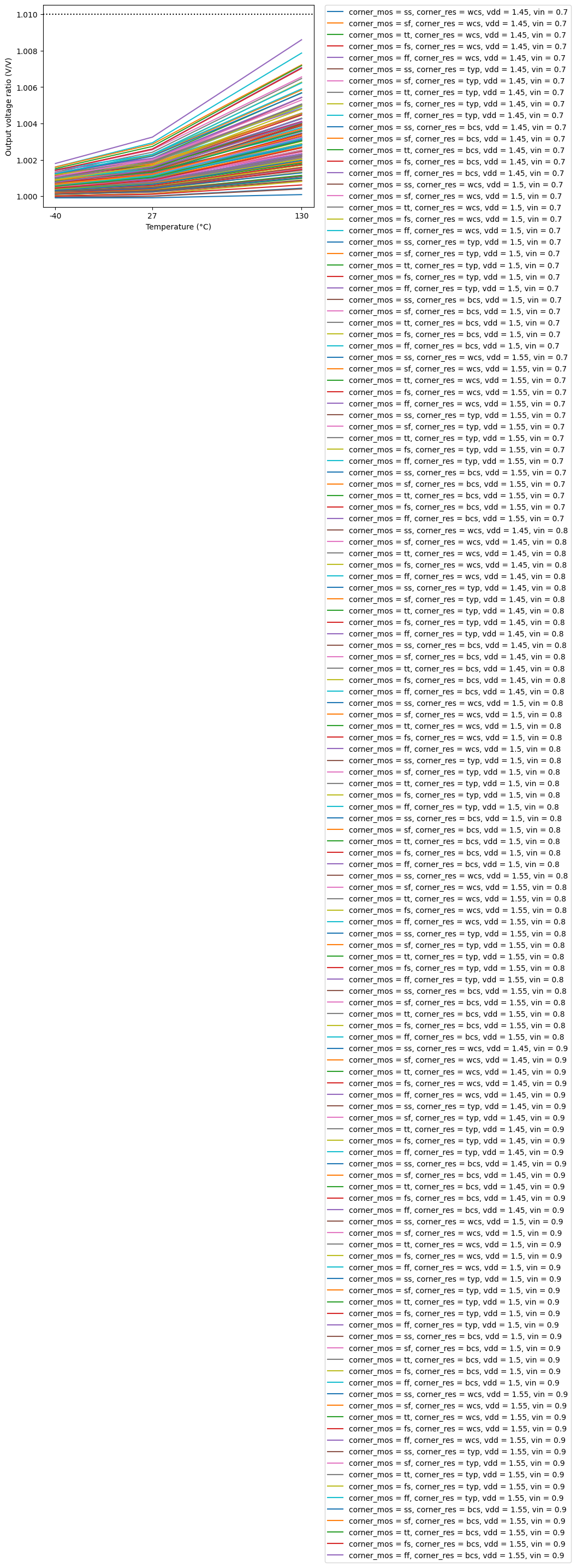
Output voltage ratio ngspice gain 0.99 V/V 1.000 V/V any 1.002 V/V 1.01 V/V 1.006 V/V Pass ✅
Bandwidth ngspice bw 10e6 Hz 146600000.000 Hz any 206653000.000 Hz any 254164000.000 Hz Pass ✅
Output voltage ratio (MC) ngspice gain_mc any 1.002 V/V any 1.002 V/V any 1.002 V/V Pass ✅
Bandwidth (MC) ngspice bw_mc 10e6 Hz 204156000.000 Hz any 207620500.000 Hz any 210269000.000 Hz Pass ✅
Output noise ngspice noise any 0.309 mV any 0.391 mV 0.6 mV 0.530 mV Pass ✅
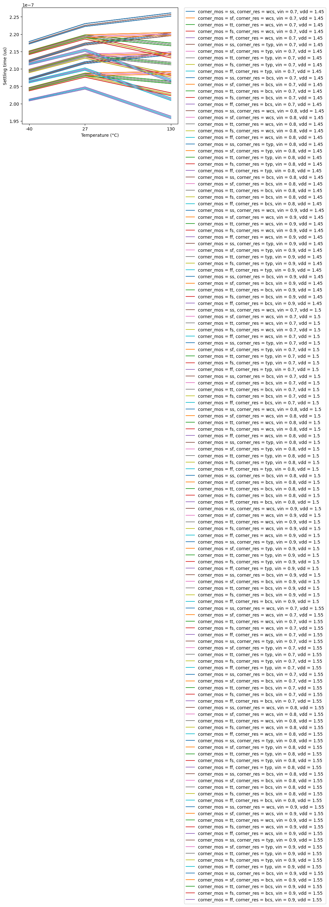
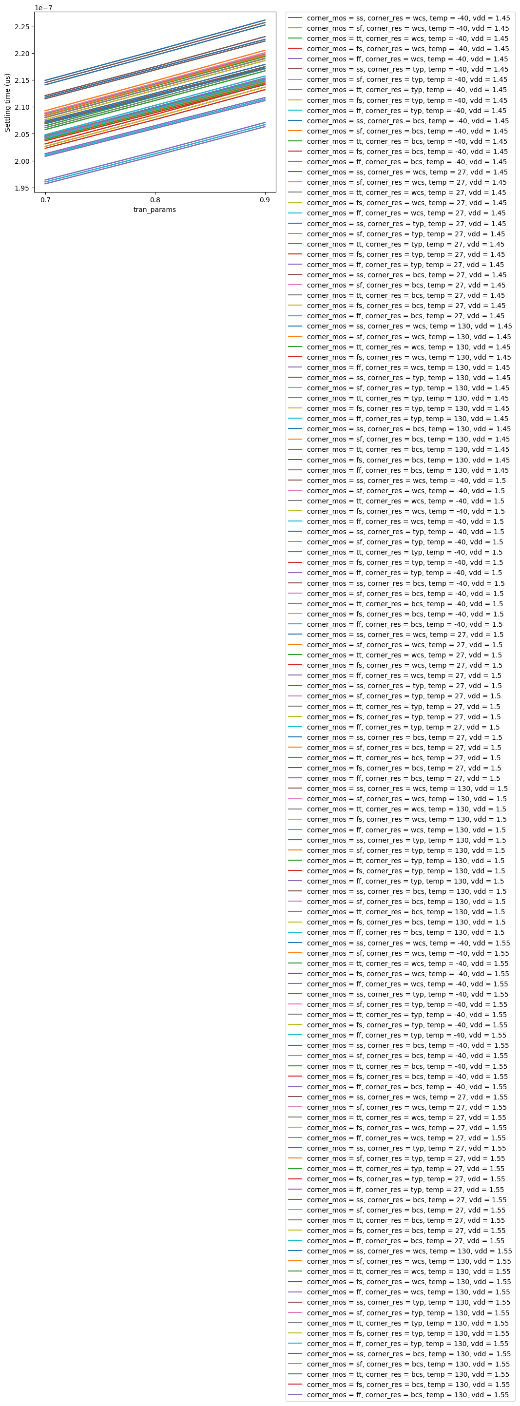
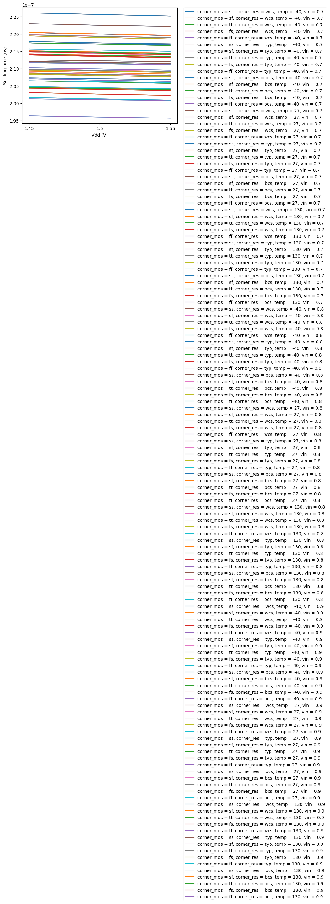
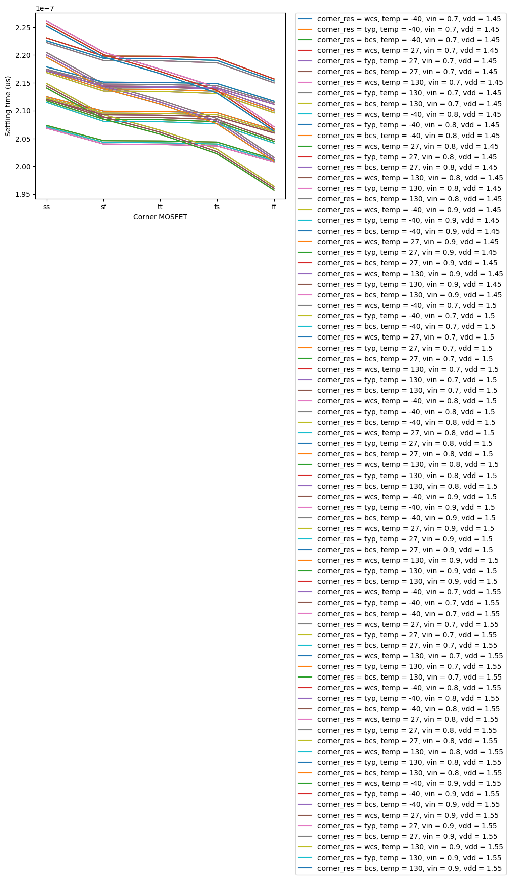
Settling time ngspice tsettle any 0.134 us any 0.141 us 1 us 0.151 us Pass ✅

Plots

gain_vs_temp

gain_vs_temp

Corner Simulation of Improved OTA

CACE Summary for Improved OTA

gain_vs_vin
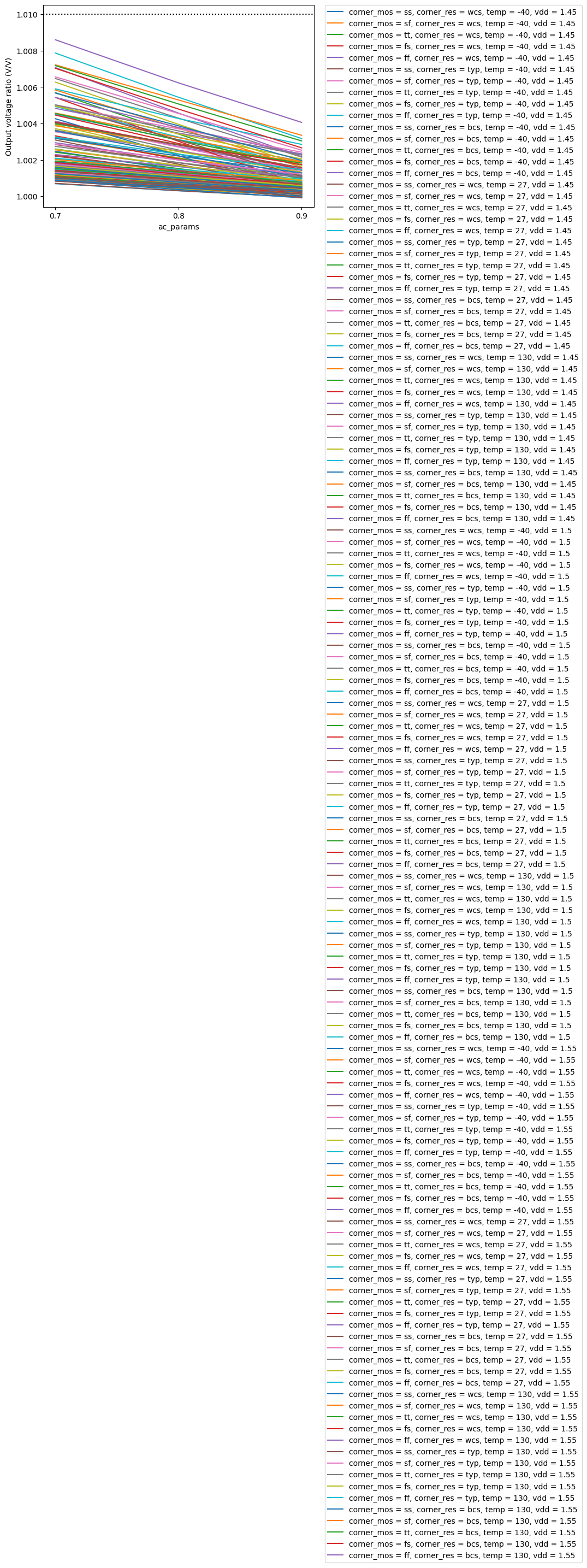
gain_vs_vin

Corner Simulation of Improved OTA

CACE Summary for Improved OTA

gain_vs_vdd
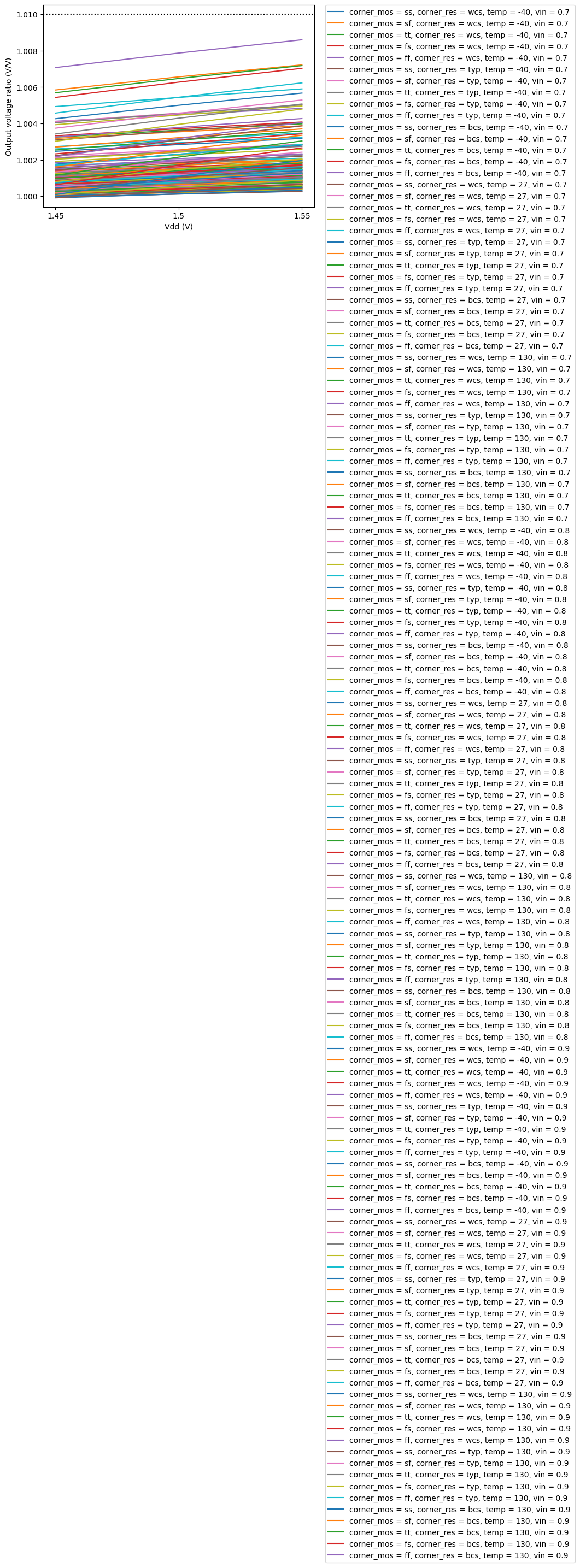
gain_vs_vdd

Corner Simulation of Improved OTA

CACE Summary for Improved OTA

gain_vs_corner
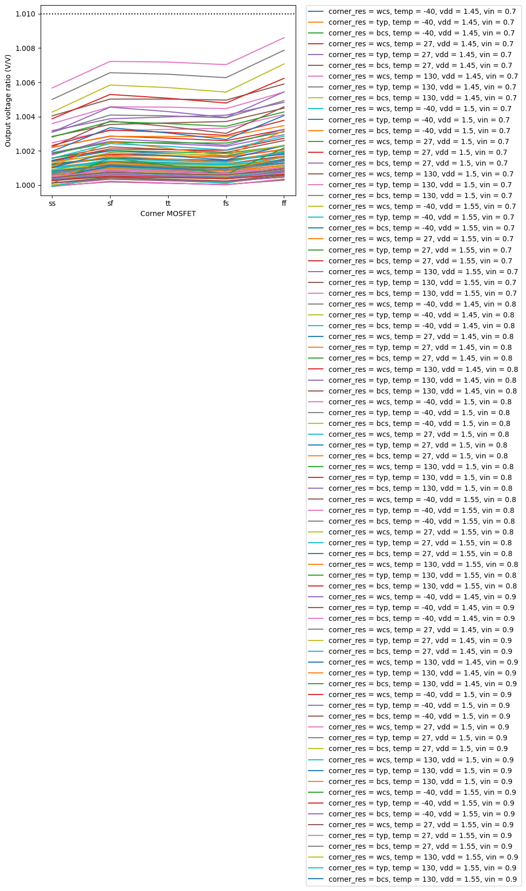
gain_vs_corner

Corner Simulation of Improved OTA

CACE Summary for Improved OTA

bw_vs_temp
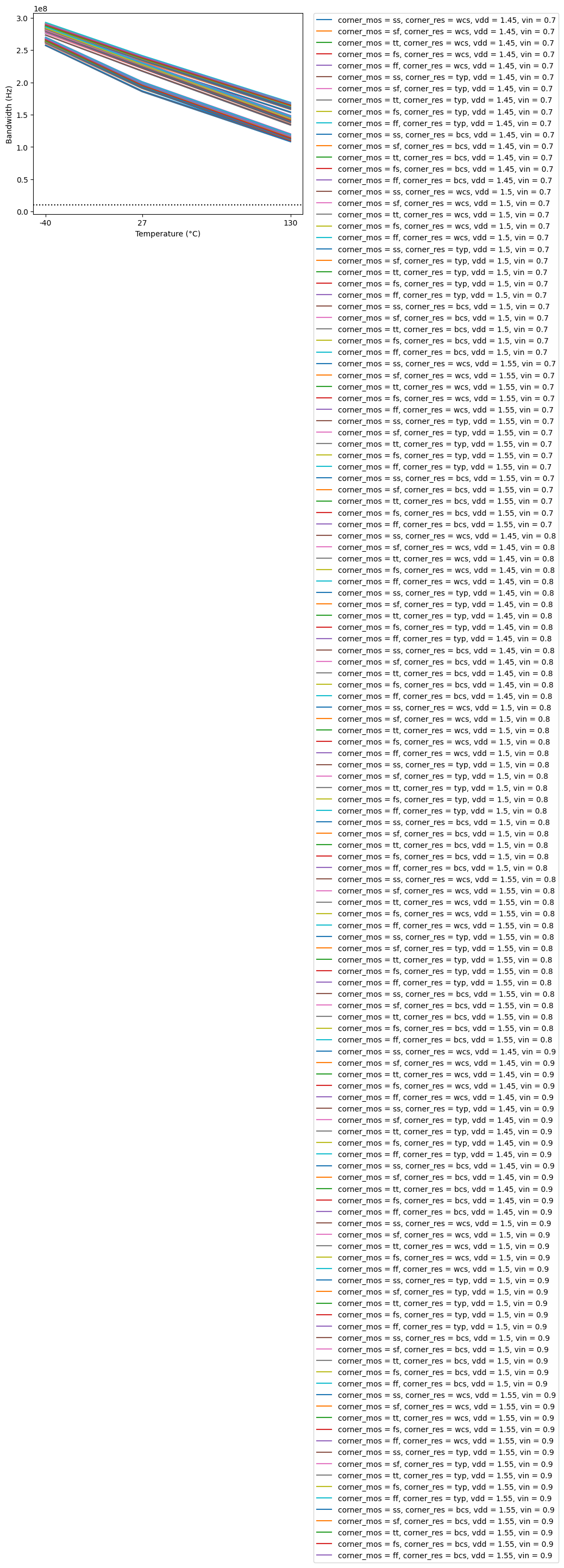
bw_vs_temp

Corner Simulation of Improved OTA

CACE Summary for Improved OTA

bw_vs_vin
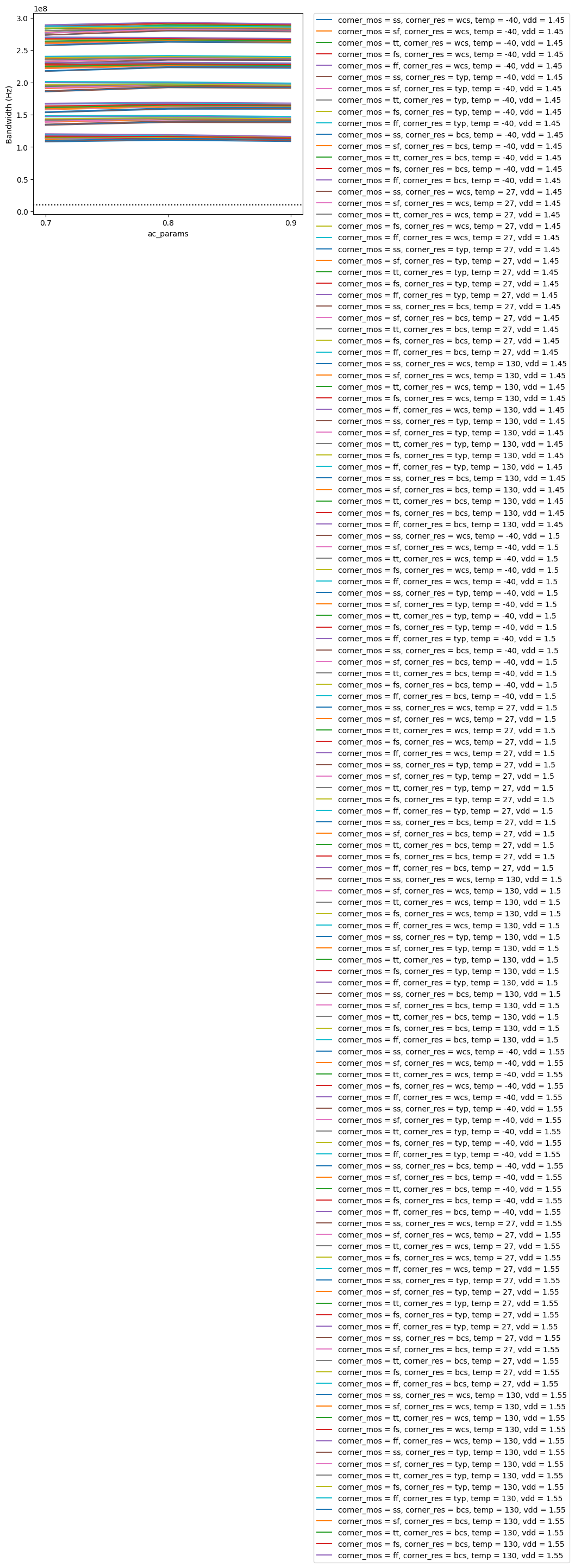
bw_vs_vin

Corner Simulation of Improved OTA

CACE Summary for Improved OTA

bw_vs_vdd
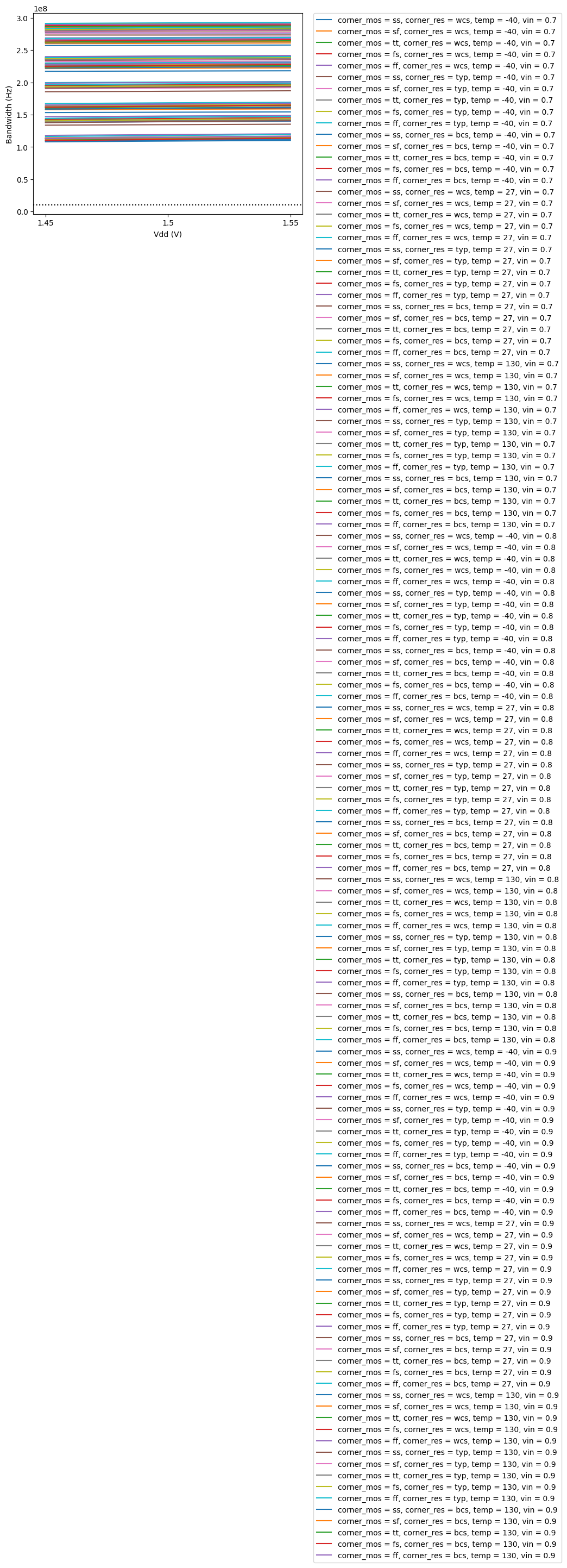
bw_vs_vdd

Corner Simulation of Improved OTA

CACE Summary for Improved OTA

bw_vs_corner
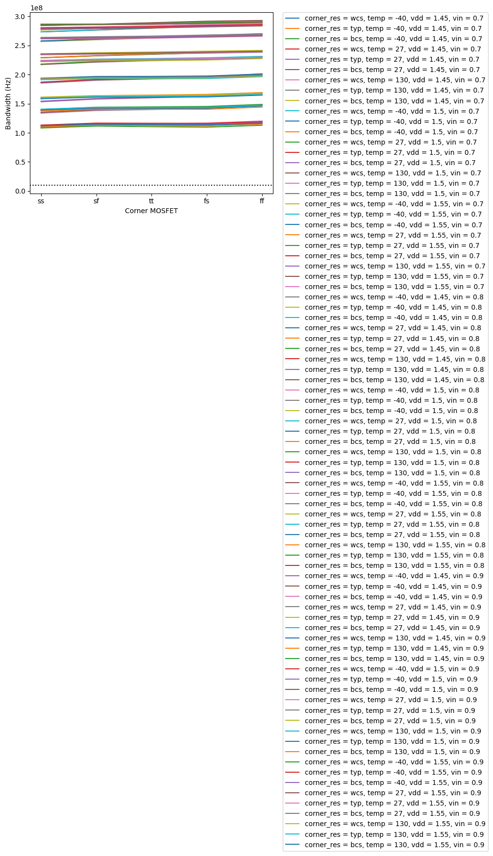
bw_vs_corner

Corner Simulation of Improved OTA

CACE Summary for Improved OTA

gain_mc
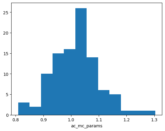
gain_mc

Corner Simulation of Improved OTA

CACE Summary for Improved OTA

bw_mc
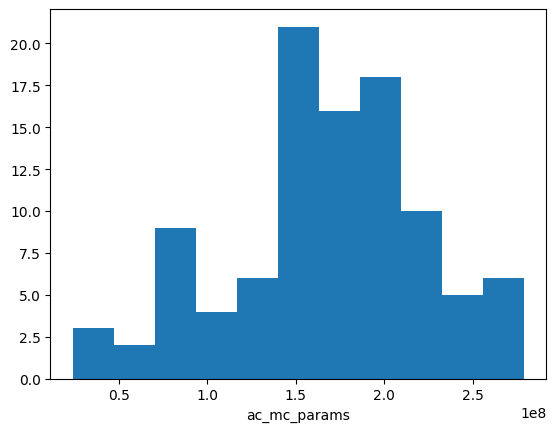
bw_mc

Corner Simulation of Improved OTA

CACE Summary for Improved OTA

noise_vs_temp
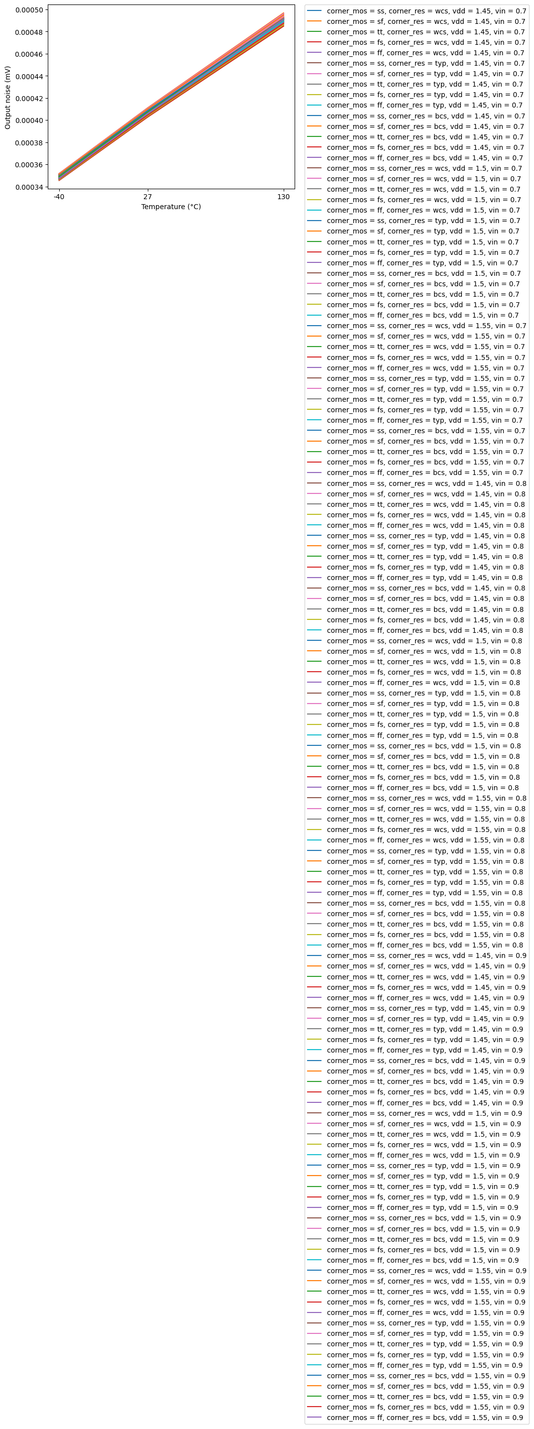
noise_vs_temp

Corner Simulation of Improved OTA

CACE Summary for Improved OTA

noise_vs_vin
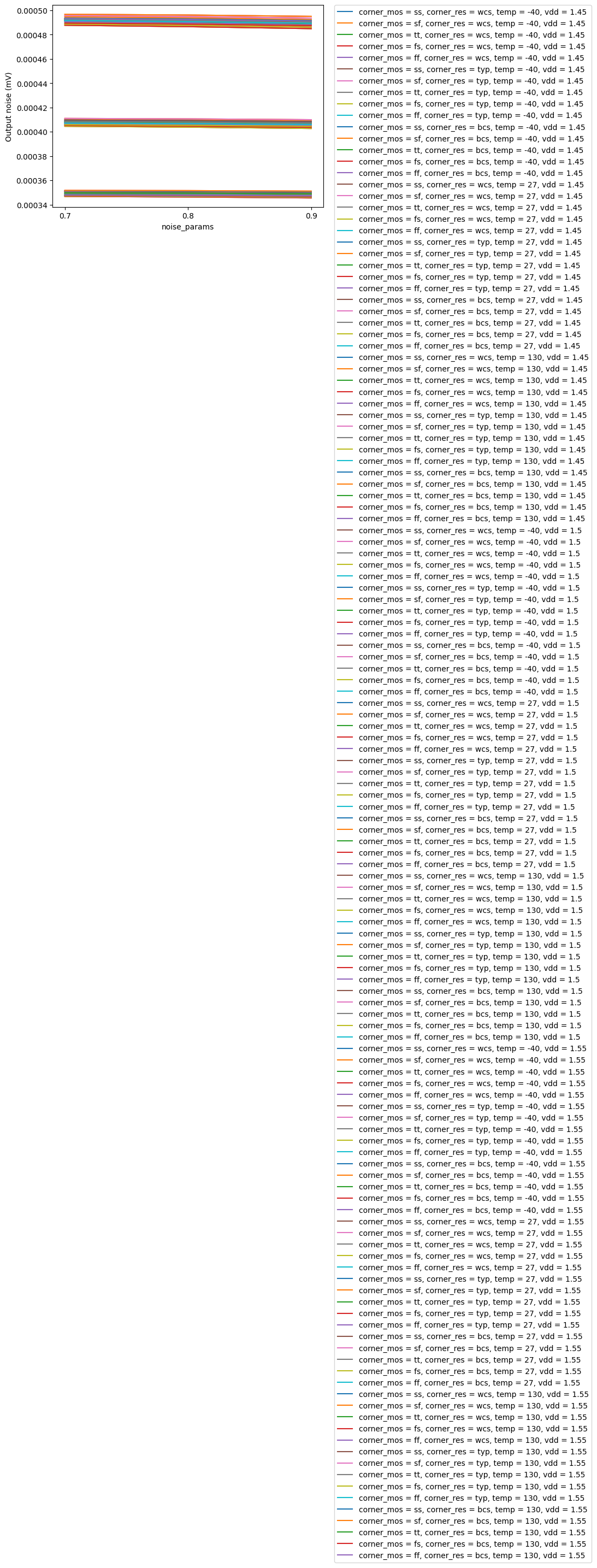
noise_vs_vin

Corner Simulation of Improved OTA

CACE Summary for Improved OTA

noise_vs_vdd
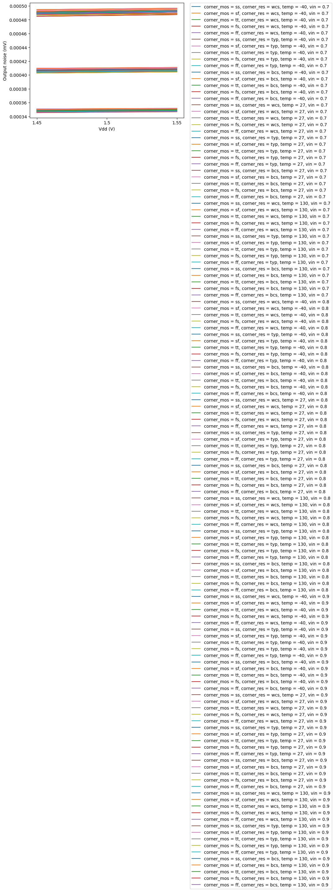
noise_vs_vdd

Corner Simulation of Improved OTA

CACE Summary for Improved OTA

noise_vs_corner
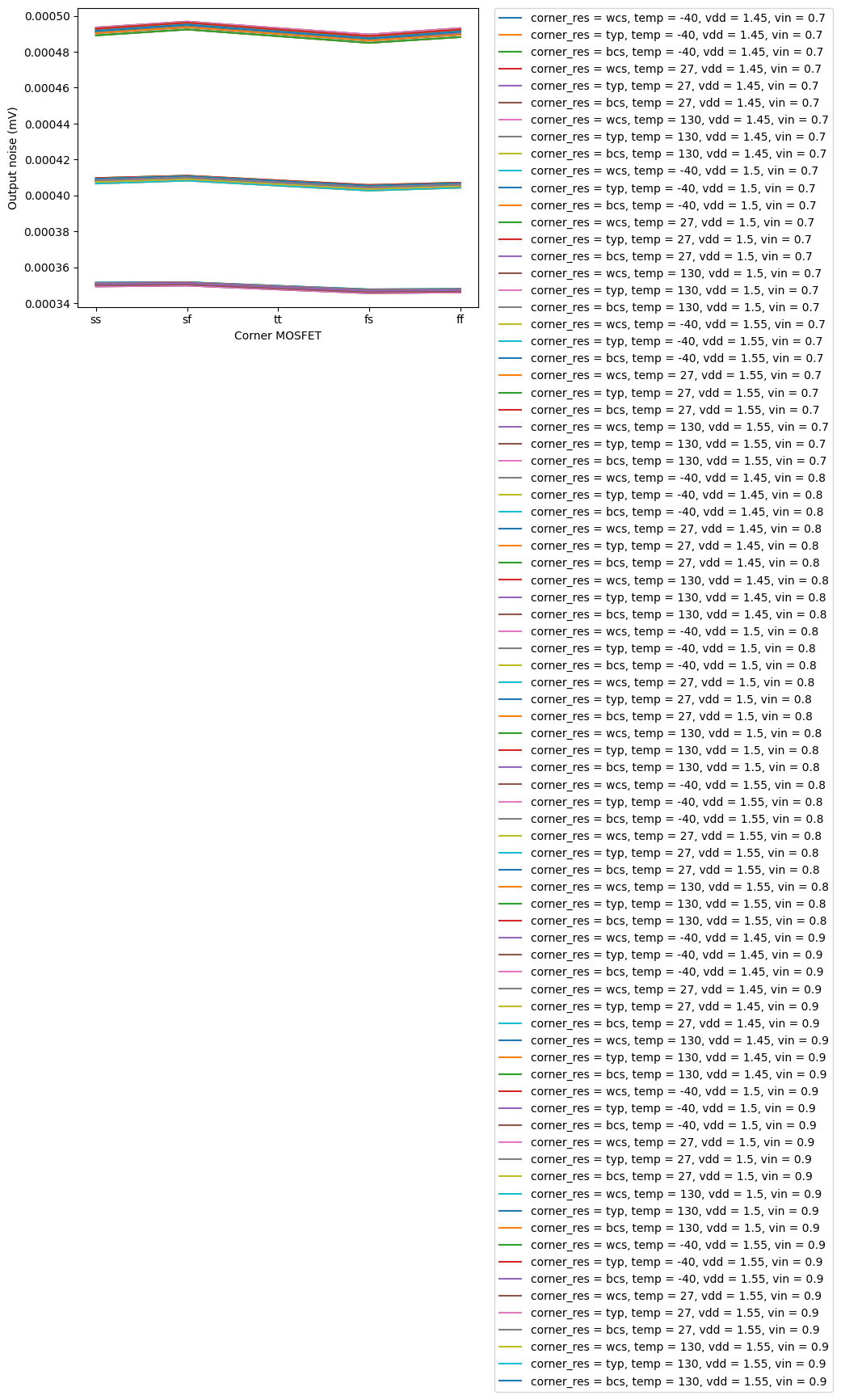
noise_vs_corner

Corner Simulation of Improved OTA

CACE Summary for Improved OTA

settling_vs_temp
settling_vs_temp

Corner Simulation of Improved OTA

CACE Summary for Improved OTA

settling_vs_vin
settling_vs_vin

Corner Simulation of Improved OTA

CACE Summary for Improved OTA

settling_vs_vdd
settling_vs_vdd

Corner Simulation of Improved OTA

CACE Summary for Improved OTA

settling_vs_corner
settling_vs_corner

Corner Simulation of Improved OTA

Table 5: Voltage buffer specification
Specification Basic 5T-OTA Improved OTA Unit
Output voltage error \(<3\) \(<1\) %
Total output noise (rms) \(<1\) \(<0.6\) mVrms
Supply current (as low as possible) \(<10\) \(<20\) µA
Turn-on time (settled to within 1%) \(<10\) \(<1\) µs
Externally provided bias current (nominal) \(20\) \(5\) µA

References

Jespers, Paul G. A., and Boris Murmann. 2017. Systematic Design of Analog CMOS Circuits: Using Pre-Computed Lookup Tables. Cambridge University Press.

References