Electrostatic Discharge and Latch-Up
Design of Complex Integrated Circuits
ESD Models for Testing
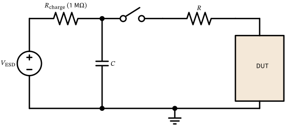
Figure 80: Equivalent circuit of the standardized ESD test models: the model capacitance \(C\) is charged to the test voltage via a high-ohmic resistor; closing the switch discharges it into the DUT through the model resistance \(R\).
ESD Models for Testing
ESD Protection Concept
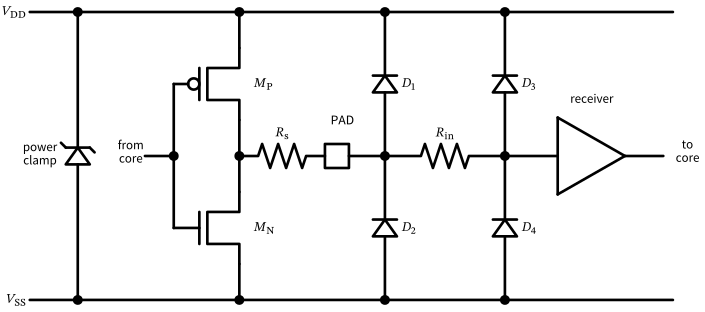
Figure 82: ESD protection of a bidirectional digital I/O pad: the primary diodes \(D_1\)/\(D_2\) carry the main discharge current to the rails, the series resistor \(R_\mathrm{in}\) limits the current into the secondary diodes \(D_3\)/\(D_4\), which protect the gate oxide of the input receiver; the output driver \(M_\mathrm{P}\)/\(M_\mathrm{N}\) is decoupled from the pad by the small drain series resistance \(R_\mathrm{s}\); the power clamp closes the discharge loop between \(V_\mathrm{DD}\) and \(V_\mathrm{SS}\).
Snapback Devices: The ggNMOS
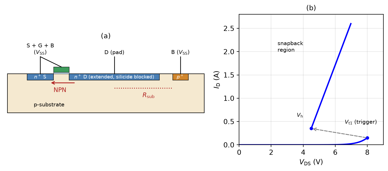
RC-Triggered Power Clamp
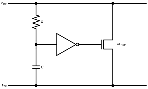
Figure 84: RC-triggered power-supply clamp: in normal operation, the capacitor is charged to \(V_\mathrm{DD}\), the inverter output is low, and the large clamp transistor \(M_\mathrm{ESD}\) is off.
The Silicon-Controlled Rectifier
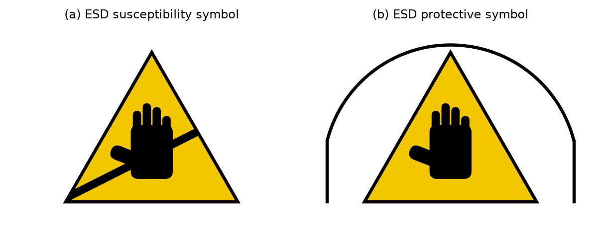
ESD-Protected Areas
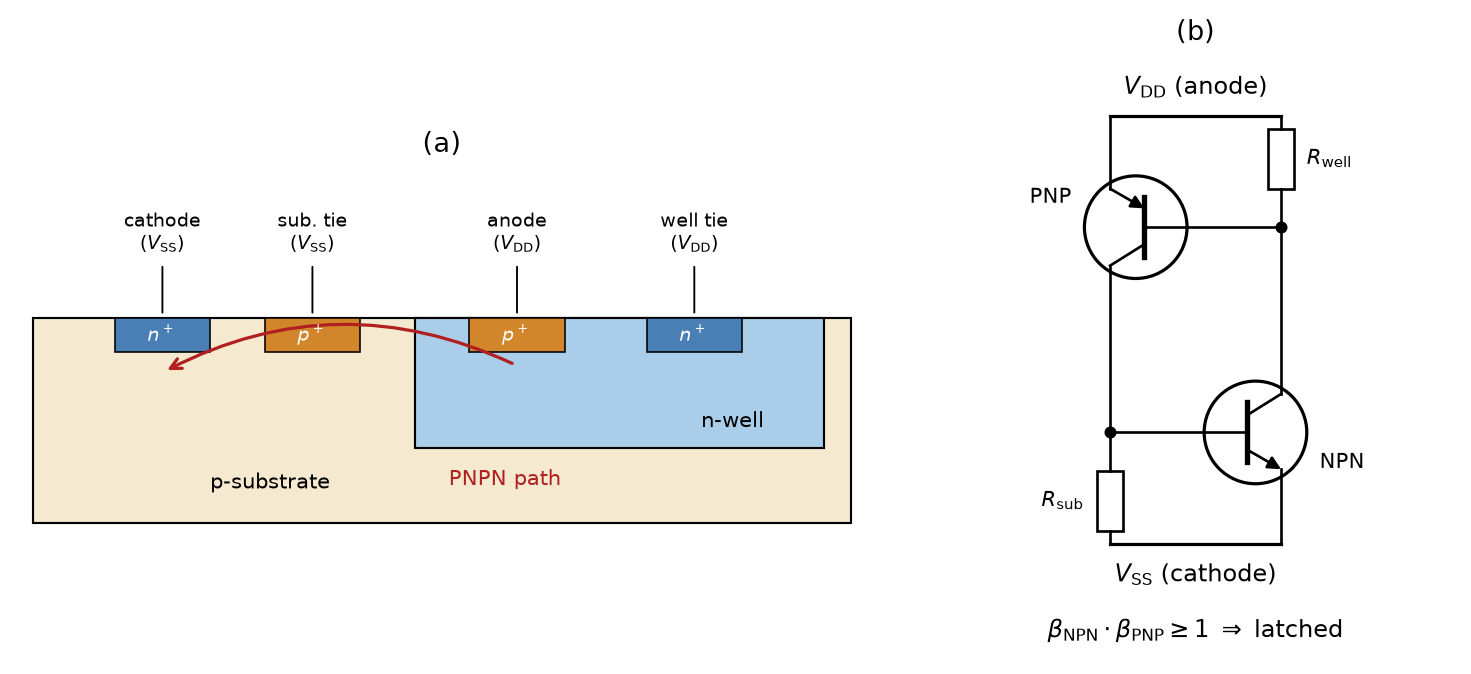
Latch-Up
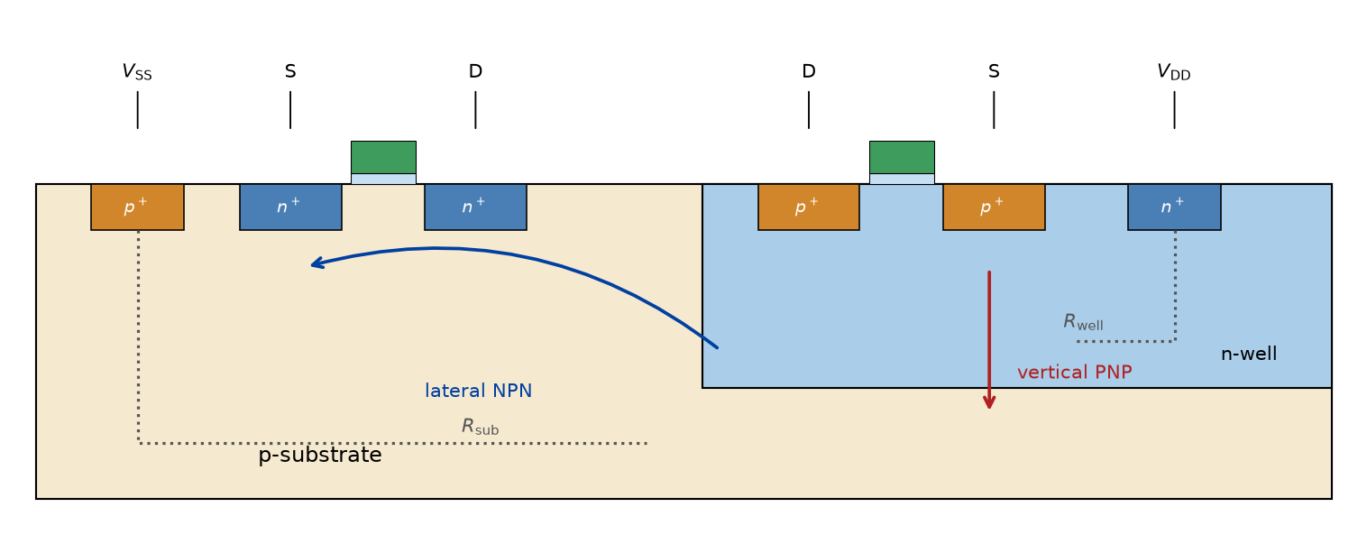
Latch-Up Prevention