
Design of Complex Integrated Circuits
1 Introduction
Integrated circuits (ICs) are ubiquitous in our modern society. The extremely high density of functions (computation, storage, signal processing, digitization, energy conversion) offered by microelectronics enables all the devices and infrastructure that we depend on: the control of factories and energy generation, computation in server farms, personal computers and mobile devices, communication by wires, optics, or wireless links, and sensing of the environment. All of these are driven by integrated circuits, implemented in various semiconductor technologies.
This course looks at integrated circuits from two complementary angles. In the first part, we discuss how ICs are built: the operation of the MOSFET, the CMOS manufacturing technology, the physical layout, packaging, production testing, and the economics of chip making. In the second part, we discuss how complex ICs are designed: design methodologies for digital and mixed-signal circuits, protection against electrostatic discharge and latch-up, robust design techniques, and the inner workings of circuit simulators.
It is assumed that readers are familiar with the contents of our Analog Circuit Design course; basic knowledge of digital and analog circuit design is a prerequisite for the later chapters.
Important
All course material (source code of this document, Python code for all figures, etc.) is made publicly available on GitHub and shared under the Apache-2.0 license.
Please feel free to submit pull requests to fix typos or add content! If you want to discuss something that is not clear, please open an issue.
The production of this document would be impossible without these (and many more) great open-source software products: VS Code, Quarto, Pandoc, LaTeX, Jupyter Notebook, Python, schemdraw, Numpy, Matplotlib, Pandas, Git, …
1.1 How Small Is a Nanometer?
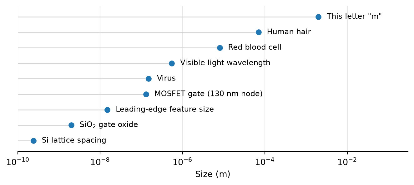
Modern CMOS technologies pattern structures with dimensions of a few nanometers. To develop a feeling for how small these dimensions really are, Figure 1 compares the feature sizes of integrated circuits with a few familiar objects: a human hair is roughly \(70\,\mu\text{m}\) thick, a red blood cell has a diameter of about \(8\,\mu\text{m}\), a virus measures around \(150\,\text{nm}\), and the distance between two silicon atoms in the crystal lattice is only \(0.24\,\text{nm}\). The minimum feature sizes of leading-edge CMOS processes are thus much smaller than a virus, and only about one order of magnitude away from the atomic spacing of the silicon crystal itself!
1.2 A Brief History of Semiconductors
The history of semiconductor electronics spans not even one century from the first observation of semiconductor rectification to today’s chips with billions of transistors. Figure 2 summarizes the key milestones which we briefly discuss in the following.
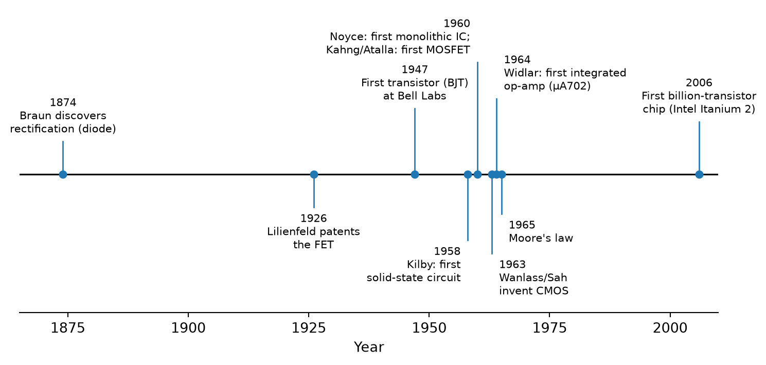
1874, the diode: Karl Ferdinand Braun discovers the rectifying effect of a particular type of mineral (galena, “Bleiglanz”). This effect is later exploited in radio receivers in the form of the crystal detector (the “cat’s whisker”), which is the first semiconductor electronic device.
1926, the field-effect transistor (FET): Julius Lilienfeld patents the field-effect transistor. Unfortunately, it takes several decades before such a device can actually be manufactured, as surface charges at the semiconductor interface cause malfunction of the early devices. Only in 1960 do Dawon Kahng and Mohamed Atalla finally demonstrate the metal-oxide-semiconductor field-effect transistor (MOSFET).
1947, the bipolar junction transistor (BJT): John Bardeen, William Shockley, and Walter Brattain demonstrate the first semiconductor transistor (using germanium) at Bell Labs. This was a big step towards the replacement of vacuum tubes. In the first point-contact transistor, the bottom piece of germanium formed the base terminal, hence the name “base.”
1958/1960, the first integrated circuit: After the first solid-state circuit demonstrated by Jack Kilby in 1958, Robert Noyce and his team at Fairchild build the first monolithic integrated circuit with pn-junction isolation in 1960: a flip-flop in transistor-resistor logic, integrated onto a wafer with 3 mm diameter.
1963, complementary MOS (CMOS): In an ISSCC paper, Frank Wanlass and Chih-Tang Sah of Fairchild Semiconductor show that logic built from p-channel and n-channel MOSFETs draws very little standby power—the invention of CMOS (Wanlass and Sah 1963).
1964, analog integrated circuits: Robert J. Widlar, the “Father of Analog Integrated Circuits,” designs the first integrated operational amplifier, the µA702.
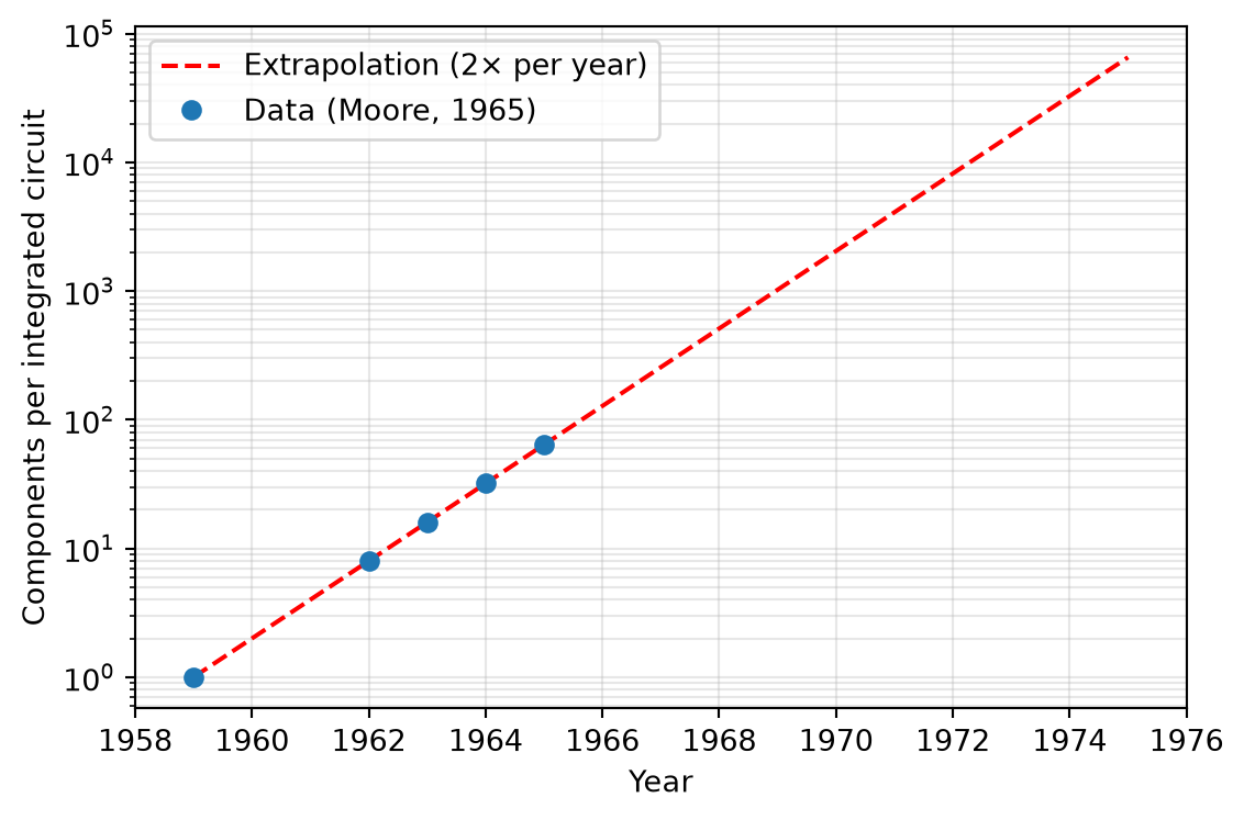
1965, Moore’s law: Gordon E. Moore, based on only a handful of data points, makes a bold prediction about the growth of the number of components per integrated circuit, which would eventually become known as “Moore’s law” (Moore 1965). Figure 3 shows the data available to Moore in 1965 together with his famous extrapolation: a doubling of the number of components per chip every year (later revised to a doubling every two years)—an exponential growth trend that the industry has followed for decades.
2006, the first billion-transistor logic chip: Intel announces the first microprocessor with more than one billion transistors, the Intel Itanium 2. The chip is manufactured in a 90 nm CMOS process and contains 1.72 billion transistors on a die with an area of 374 mm². The first demonstrated chip with one billion transistors is a 1 Gbit DRAM presented by NEC in 1995, manufactured in 0.25 µm technology (Sugibayashi et al. 1995).
For an excellent, much more detailed account of semiconductor history, visit the Silicon Engine timeline of the Computer History Museum.
2 The MOSFET
This chapter on the metal-oxide-semiconductor field-effect transistor (MOSFET) is largely based on (Hu 2010; Razavi 2014; Tsividis and McAndrew 2011), which are also recommended as further reading. In contrast to our Analog Circuit Design course, where we treated the MOSFET essentially as a numerically-characterized black box, we will derive a simple, first-order model of the MOSFET from the physics of the device, and then discuss the most important second-order effects. The goal is to understand the basic operation of the MOSFET and its \(I\)/\(V\) characteristic, which will be used in later chapters for circuit design.
2.1 MOSFET Operation in a Nutshell
The basic MOSFET structure consists of a gate (terminal \(G\)) that is insulated from a doped semiconductor and controls the surface charge in the semiconductor channel below, between the source (terminal \(S\)) and the drain (terminal \(D\)). The source provides the charge carriers, and an electric field pulls them toward the drain (hence a semiconductor device based on drift current). The electric potential of the semiconductor bulk (terminal \(B\)) acts on the channel as well and is the fourth terminal of the MOSFET. Ideally, the effect of the bulk is negligible.
Two complementary flavors of the device exist: the \(n\)-type MOSFET (“NMOS”) has \(n^+\)-doped source/drain regions on a \(p\)-type substrate and usually an \(n^{++}\)-doped gate, while the \(p\)-type MOSFET (“PMOS”) has \(p^+\)-doped source/drain regions in an \(n\)-type well and usually a \(p^{++}\)-doped gate.
NoteDoping Notation
In the doping notation, \(+\) indicates a higher doping concentration than the surrounding material, while \(++\) indicates an even higher doping concentration. For example, \(n^+\)-doped regions have a higher electron concentration than the \(n\)-type substrate, and \(n^{++}\)-doped gates have an even higher electron concentration than the \(n^+\)-doped source/drain regions.
To understand the operation of the NMOS transistor, it is instructive to follow the conditions in the semiconductor while the gate voltage is swept upwards, as illustrated in Figure 4:
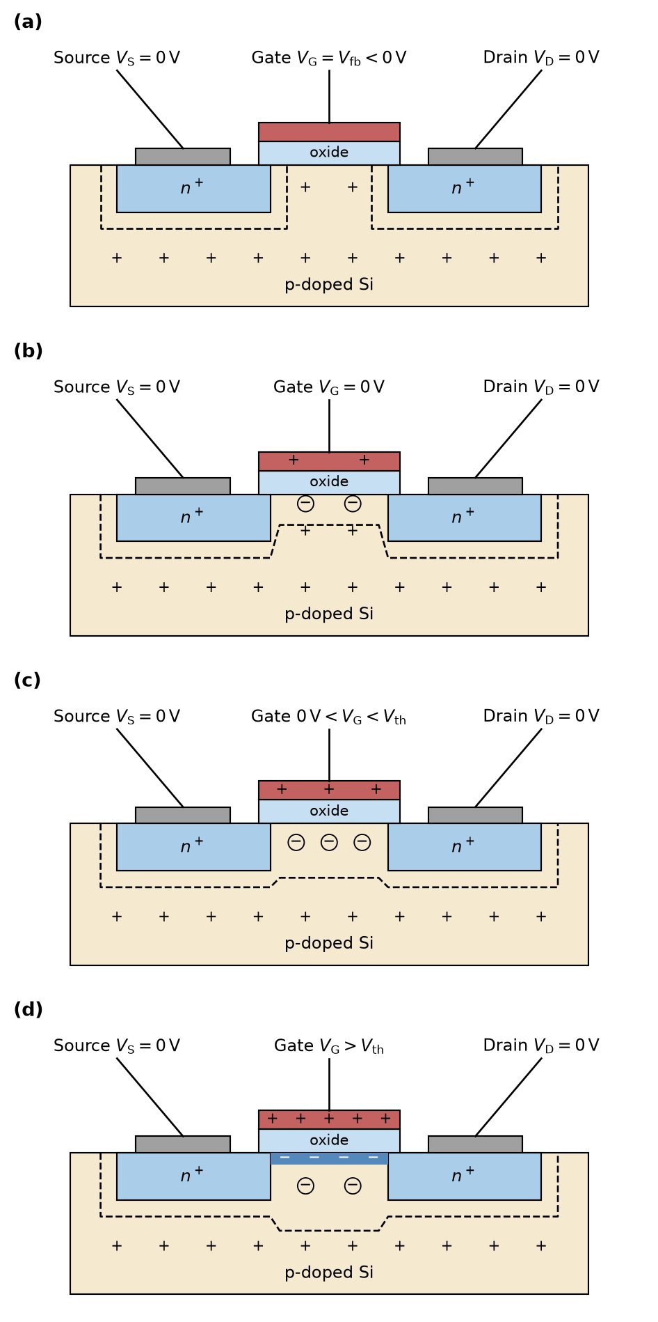
- Flatband (a): When the gate is at a specific negative voltage (the flatband voltage \(V_\mathrm{fb}\)), and all other terminals are at \(0\,\text{V}\), a depletion zone forms only around the drain and source junctions. No current can flow, since drain and source are \(n^+\)-doped while the substrate is \(p\)-type, so the two junctions form back-to-back diodes.
- Zero gate voltage (b): When the gate voltage is increased to \(0\,\text{V}\), a depletion zone also forms below the gate. The \(p\)-type acceptor ions in this region have captured an electron and are thus immobile, negatively charged sites (illustrated by the circled minus symbols)—still, no current can flow.
- Below threshold (c): When the gate voltage increases further (but stays below the threshold voltage), the depletion zone below the gate deepens, reaching a maximum depletion width \(W_\mathrm{dep}\) when \(V_\mathrm{GS}= V_\mathrm{th}\). There is still no conduction between drain and source, because there are no (or at least very few) free electrons in the channel region.
- Inversion (d): When the gate voltage rises above the threshold voltage \(V_\mathrm{th}\), inversion occurs: a thin layer of free electrons forms directly below the gate oxide, creating a conducting channel of electrons between drain and source. The source of the electrons in the inversion layer is the \(n^+\)-doped source region, which is connected to ground. The electrons are pulled from the source into the channel by the positive gate voltage, and they can now flow to the drain if a drain voltage is applied.
Once the channel exists, the drain voltage determines the mode of conduction, as shown in Figure 5:
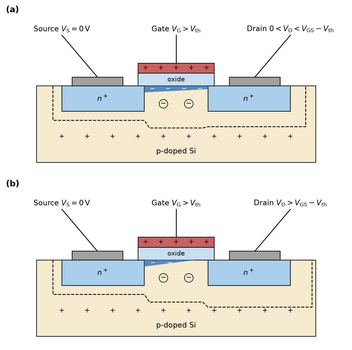
- Triode (a): If a small voltage is applied between drain and source, a current flows, and the depletion zone around the drain widens. The drain current is a function of both \(V_\mathrm{GS}\) and \(V_\mathrm{DS}\); the device operates in the triode region. The MOSFET operates like a voltage-controlled resistor in this region.
- Saturation (b): If the drain-source voltage is increased beyond \(V_\mathrm{DS}> V_\mathrm{GS}- V_\mathrm{th}\), the channel is pinched off at the drain side, and the drain current is (to first order) no longer a function of \(V_\mathrm{DS}\), only of \(V_\mathrm{GS}\)—the device is now in saturation. The MOSFET operates like a voltage-controlled current source in this region.
2.1.1 An Exemplary 130 nm Process Technology
Throughout this text we will use typical parameters of a 0.13 µm CMOS process technology, specifically IHP SG13 (process specification), for exemplary calculations. The key parameters are listed in Table 1.
| Parameter | Symbol | Typical value |
|---|---|---|
| Nominal supply voltage | \(V_\mathrm{DD}\) | 1.2 V (digital) / 1.5 V (analog) |
| Minimum gate length | \(L_\mathrm{min}\) | 130 nm |
| Oxide thickness | \(t_\mathrm{ox}\) | 2 nm |
| Threshold voltage NMOS | PMOS | \(V_\mathrm{th,n}\) | \(V_\mathrm{th,p}\) | 0.5 V | −0.47 V |
| Maximum voltage | \(|V_\mathrm{GS,max}|\), \(|V_\mathrm{DS,max}|\) | 2 V |
| Gate capacitance | \(C'_\mathrm{ox}\) | 17.3 fF/µm² |
| Process constant \(K_\mathrm{n}\) | \(K_\mathrm{p}\) | \(\mu_\mathrm{n}C'_\mathrm{ox}\) | \(\mu_\mathrm{p}C'_\mathrm{ox}\) | 280 µA/V² | 130 µA/V² |
2.2 Basic I/V Characteristic of the MOSFET
2.2.1 The MOS Capacitor and the Threshold Voltage
If source, drain, and substrate are grounded (\(V_\mathrm{S} = V_\mathrm{D} = V_\mathrm{B} = 0\,\text{V}\)), and a positive voltage \(V_\mathrm{GS}= V_\mathrm{G}\) is applied to the gate, then positive charge accumulates on the gate and negative charge in the \(p\)-type substrate, forming a depletion layer in the substrate.
If we assume a uniform charge density \(\rho = -q N_\mathrm{a}\) across this layer with \(N_\mathrm{a}\) being the doping concentration of the \(p\)-type substrate (in a practical device, this charge density is not uniform), then we can use Poisson’s equation. Note that with the boundary conditions assuming \(\Phi(0) = 0\) and \(d\Phi(0)/dy = 0\), \(y=0\) is the point where the depletion layer starts in the depth of the substrate, and \(y = W_\mathrm{dep}\) is the point where the depletion layer ends (the depletion width) at the substrate-oxide interface (\(\varepsilon_\mathrm{si}\) is the permittivity of silicon):
\[ \frac{d^2 \Phi(y)}{d y^2} = -\frac{\rho(y)}{\varepsilon_\mathrm{si}} = \frac{q N_\mathrm{a}}{\varepsilon_\mathrm{si}} \quad \rightarrow \quad \Phi(y) = \frac{q N_\mathrm{a}}{2 \varepsilon_\mathrm{si}} y^2 \tag{1}\]
The surface potential \(\Phi_\mathrm{S}= \Phi(W_\mathrm{dep})\) at the oxide-silicon interface is then related to the depletion width \(W_\mathrm{dep}\) by
\[ W_\mathrm{dep}= \sqrt{\frac{2 \varepsilon_\mathrm{si}\Phi_\mathrm{S}}{q N_\mathrm{a}}}. \tag{2}\]
With \(W_\mathrm{dep}\) we can also calculate the corresponding depletion capacitance (per unit area, indicated with the prime):
\[ C'_\mathrm{dep}= \frac{\varepsilon_\mathrm{si}}{W_\mathrm{dep}} = \sqrt{\frac{q N_\mathrm{a}\varepsilon_\mathrm{si}}{2 \Phi_\mathrm{S}}} \tag{3}\]
The charge per unit area \(Q'_\mathrm{dep}\) in this region is (negative, because of the captured electrons)
\[ Q'_\mathrm{dep} = - q N_\mathrm{a}W_\mathrm{dep}= - \sqrt{2 q N_\mathrm{a}\varepsilon_\mathrm{si}\Phi_\mathrm{S}} \tag{4}\]
The gate voltage is the result of the sum of the flatband voltage, the surface potential, and the voltage across the oxide
\[ V_\mathrm{G} = \Phi_\mathrm{fb}+ \Phi_\mathrm{S}+ V_\mathrm{ox} = \Phi_\mathrm{fb0} + \frac{-Q'_\mathrm{ss}}{C'_\mathrm{ox}} + \Phi_\mathrm{S}+ \frac{-Q'_\mathrm{sub}}{C'_\mathrm{ox}} \tag{5}\]
where \(\Phi_\mathrm{fb}\) is the work-function difference between the gate and the substrate material (the flatband voltage \(V_\mathrm{fb}\) used in Figure 4). Note that the negative sign in the last term arises because voltage and charge are taken from different electrodes of the gate capacitor: the voltage \(V_\mathrm{ox}\) at the top, and the substrate charge \(Q'_\mathrm{sub}\) as well as the interface charge \(Q'_\mathrm{ss}\) at the bottom.
An interface charge \(Q'_\mathrm{ss}\) can be present at the SiO2-Si interface due to crystal discontinuities. This interface charge can be accounted for by adapting the flatband voltage \(\Phi_\mathrm{fb0}\) to \(\Phi_\mathrm{fb}\) (going forward, we will just use \(\Phi_\mathrm{fb}\)).
Using Equation 2 to express \(\Phi_\mathrm{S}= q N_\mathrm{a}W_\mathrm{dep}^2 / (2 \varepsilon_\mathrm{si})\) and Equation 4 for \(Q'_\mathrm{sub} = Q'_\mathrm{dep}\), Equation 5 can be written as
\[ V_\mathrm{G} = \Phi_\mathrm{fb}+ \frac{q N_\mathrm{a}W_\mathrm{dep}^2}{2 \varepsilon_\mathrm{si}} + \frac{q N_\mathrm{a}W_\mathrm{dep}}{C'_\mathrm{ox}} \tag{6}\]
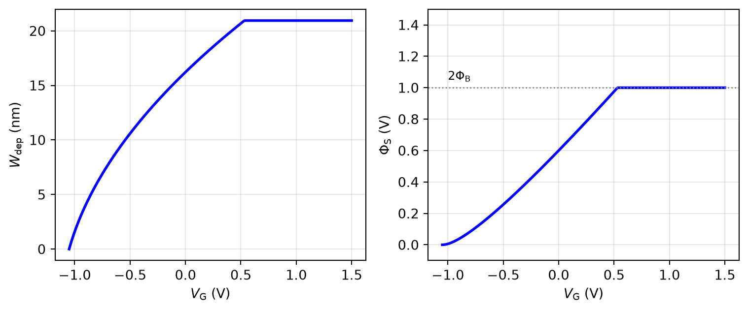
From Equation 6, the depletion width \(W_\mathrm{dep}\) can be calculated as a function of \(V_\mathrm{G}\), and from this \(\Phi_\mathrm{S}= f(V_\mathrm{G})\) using Equation 2.
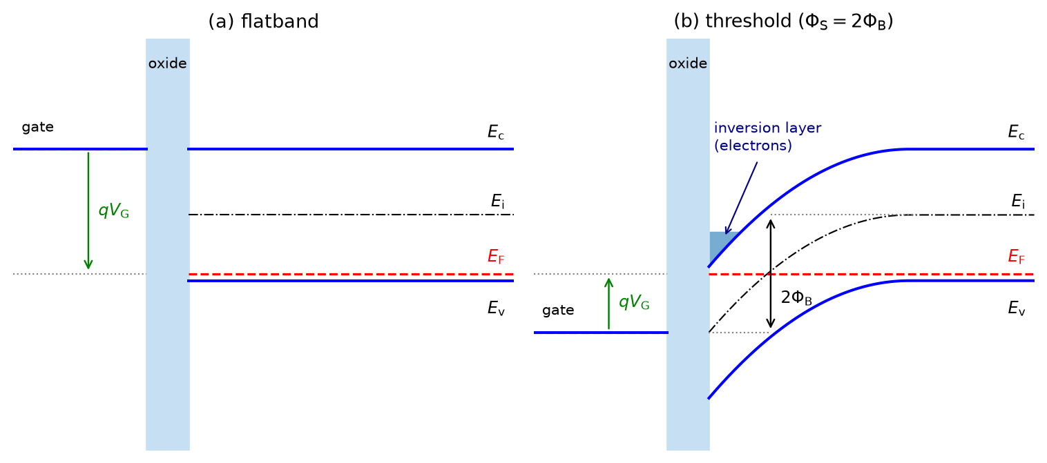
If the surface potential \(\Phi_\mathrm{S}\) reaches a critical level of twice the Fermi potential \(\Phi_\mathrm{B}\), then inversion occurs: a thin layer of electrons is induced directly under the oxide. The gate voltage that is minimally required to produce this inversion layer is called the threshold voltage \(V_\mathrm{th}= V_\mathrm{G}(\Phi_\mathrm{S}= 2 \Phi_\mathrm{B})\).
\[ V_\mathrm{th}= \Phi_\mathrm{fb}+ 2 \Phi_\mathrm{B}+ \frac{-Q'_\mathrm{dep}}{C'_\mathrm{ox}} = \Phi_\mathrm{fb}+ 2 \Phi_\mathrm{B}+ \frac{\sqrt{2 q N_\mathrm{a}\varepsilon_\mathrm{si}\cdot 2 \Phi_\mathrm{B}}}{C'_\mathrm{ox}} \tag{7}\]
with the Fermi potential
\[ \Phi_\mathrm{B}= \frac{k T}{q} \ln \frac{N_\mathrm{a}}{n_\mathrm{i}}. \tag{8}\]
Figure 6 illustrates the flatband and the threshold condition in terms of the energy bands of the MOS structure.
Note 1: Example Calculation of the Threshold Voltage
Let us assume a substrate doping level of \(N_\mathrm{a}= 3 \times 10^{18}\,\text{cm}^{-3}\). The Fermi potential can be calculated with Equation 8 (using the intrinsic carrier concentration of silicon \(n_\mathrm{i} = 1.0 \times 10^{10}\,\text{cm}^{-3}\) at room temperature \(T = 300\,\text{K}\)):
\[ \Phi_\mathrm{B}= \frac{k T}{q} \ln \frac{N_\mathrm{a}}{n_\mathrm{i}} = 0.50\,\text{V} \]
We further use \(C'_\mathrm{ox}= \varepsilon_\mathrm{ox}/ t_\mathrm{ox}= 17.3\,\text{fF}/\mu\text{m}^2\) for a \(t_\mathrm{ox}= 2\,\text{nm}\) gate oxide. The flatband voltage for an \(n^+\)-polysilicon gate on the \(p\)-substrate with doping \(N_\mathrm{a}\) is (with the silicon band-gap voltage \(\Phi_\mathrm{bg} = 1.12\,\text{V}\))
\[ \Phi_\mathrm{fb}= -\frac{\Phi_\mathrm{bg}}{2} - \Phi_\mathrm{B}= -1.06\,\text{V} \]
The resulting threshold voltage is thus (beware of units!)
\[ V_\mathrm{th}= \Phi_\mathrm{fb}+ 2 \Phi_\mathrm{B}+ \frac{\sqrt{2 q N_\mathrm{a}\varepsilon_\mathrm{si}\cdot 2 \Phi_\mathrm{B}}}{C'_\mathrm{ox}} = 0.53\,\text{V} \]
Using these values, we can also calculate the depletion width \(W_\mathrm{dep}\) in inversion, and the corresponding \(C'_\mathrm{dep}\) (compare \(W_\mathrm{dep}\) to \(t_\mathrm{ox}\), and \(C'_\mathrm{dep}\) to \(C'_\mathrm{ox}\)):
\[ W_\mathrm{dep}= \sqrt{\frac{2 \varepsilon_\mathrm{si}\cdot 2 \Phi_\mathrm{B}}{q N_\mathrm{a}}} = 21.0\,\text{nm} \quad \text{and} \quad C'_\mathrm{dep}= \frac{\varepsilon_\mathrm{si}}{W_\mathrm{dep}} = 5.0\,\text{fF}/\mu\text{m}^2 \]
Using Equation 6 and Equation 2 we can now visualize the depletion width \(W_\mathrm{dep}\) and the surface potential \(\Phi_\mathrm{S}\) as a function of the gate potential \(V_\mathrm{G}\), shown in Figure 7. Note how the surface potential saturates at \(2\Phi_\mathrm{B}\) once inversion is reached: any additional gate charge is then mirrored by electrons in the inversion layer rather than by a deeper depletion region.
2.2.2 Derivation of the I/V Characteristic
If we now apply a small \(V_\mathrm{DS}\), then a sufficiently large \(V_\mathrm{GS}> V_\mathrm{th}\) builds up the inversion charge \(Q'_\mathrm{inv} = C'_\mathrm{ox}(V_\mathrm{GS}- V_\mathrm{th})\) in the channel below the gate, which is then moved from source to drain by the electric field caused by \(V_\mathrm{DS}\), resulting in the drift current \(I_\mathrm{D}\) (\(\mu_\mathrm{n}\) is the electron mobility):
\[ I_\mathrm{D}= W Q'_\mathrm{inv} v = W Q'_\mathrm{inv} \mu_\mathrm{n}E = W Q'_\mathrm{inv} \mu_\mathrm{n}\frac{V_\mathrm{DS}}{L} = \mu_\mathrm{n}C'_\mathrm{ox}\frac{W}{L} (V_\mathrm{GS}- V_\mathrm{th}) V_\mathrm{DS} \tag{9}\]
If \(V_\mathrm{DS}\) increases further, the channel charge \(Q'_\mathrm{inv}(x)\) becomes a function of the position in the channel, because the drain current causes a potential gradient \(dV_\mathrm{cs}/dx\) along the channel (we assume that \(V_\mathrm{DS}\) is small enough so that the whole channel is still inverted). \(x=0\) is the source end of the channel, and \(x=L\) is the drain end.
\[ I_\mathrm{D}= W Q'_\mathrm{inv}(x) v = W C'_\mathrm{ox}( V_\mathrm{GS}- V_\mathrm{cs} - V_\mathrm{th}) \mu_\mathrm{n}\frac{dV_\mathrm{cs}}{dx} \]
Integrating along the channel from source to drain,
\[ \int_{0}^{L} I_\mathrm{D}\, dx = \mu_\mathrm{n}C'_\mathrm{ox}W \int_{0}^{V_\mathrm{DS}} ( V_\mathrm{GS}- V_\mathrm{cs} - V_\mathrm{th}) \, dV_\mathrm{cs}, \]
yields the well-known square-law characteristic
\[ I_\mathrm{D}= \mu_\mathrm{n}C'_\mathrm{ox}\frac{W}{L} \left[ ( V_\mathrm{GS}- V_\mathrm{th}) V_\mathrm{DS}- \frac{1}{2} V_\mathrm{DS}^2 \right]. \tag{10}\]
Note that this simple derivation of the MOSFET I/V characteristic is only valid for long-channel devices (\(L > 1\,\mu\text{m}\)) and does not account for second-order effects such as channel-length modulation, body effect, velocity saturation, mobility degradation with the vertical field, and subthreshold conduction. These effects will be discussed in the next section.
2.2.3 Triode Region
Equation 10 is valid only for classical, long-channel (\(L > 1\,\mu\text{m}\)) devices, and only as long as \(V_\mathrm{DS}\leq V_\mathrm{GS}- V_\mathrm{th}= V_\mathrm{od}\); this range of operation is the so-called triode region. The overdrive voltage
\[ V_\mathrm{od}= V_\mathrm{GS}- V_\mathrm{th} \tag{11}\]
is a frequently used quantity. The ratio \(W/L\) is a dimensionless quantity called the aspect ratio of the MOSFET—note that only the relative sizing of \(W\) and \(L\) impacts the transistor’s \(I\)/\(V\) characteristic!
For \(V_\mathrm{DS}\ll V_\mathrm{GS}- V_\mathrm{th}\), we can simplify Equation 10 and see that the MOSFET behaves like a voltage-controlled resistor:
\[ I_\mathrm{D}\approx \mu_\mathrm{n}C'_\mathrm{ox}\frac{W}{L} ( V_\mathrm{GS}- V_\mathrm{th}) V_\mathrm{DS}\quad \rightarrow \quad g_\mathrm{ds}= \frac{1}{r_\mathrm{o}}= \frac{\partial I_\mathrm{D}}{\partial V_\mathrm{DS}} = \mu_\mathrm{n}C'_\mathrm{ox}\frac{W}{L} ( V_\mathrm{GS}- V_\mathrm{th}) \tag{12}\]
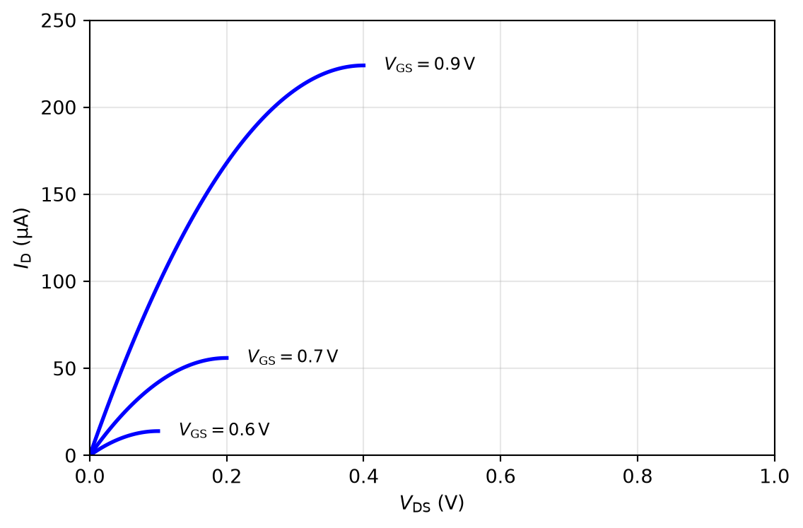
Figure 8 shows the resulting output characteristic in the triode region for three different gate voltages.
2.2.4 Saturation Region
If \(V_\mathrm{DS}> V_\mathrm{GS}- V_\mathrm{th}\), the assumption of a completely inverted channel leading up to Equation 10 is no longer valid. The channel gets pinched off at the drain side; this happens at \(V_\mathrm{DS,sat} = V_\mathrm{GS}- V_\mathrm{th}\), leading to a maximum (saturated) value of the drain current. Substituting \(V_\mathrm{DS}= V_\mathrm{DS,sat}\) into Equation 10 gives the drain current in the saturation region:
\[ I_\mathrm{D}= I_\mathrm{DS,sat} = \frac{1}{2} \mu_\mathrm{n}C'_\mathrm{ox}\frac{W}{L} ( V_\mathrm{GS}- V_\mathrm{th})^2 \tag{13}\]
In the saturation region, the MOSFET behaves like a voltage-controlled current source, so it is useful to define the transconductance
\[ g_\mathrm{m}= \frac{\partial I_\mathrm{D}}{\partial V_\mathrm{GS}}, \]
which can be expressed in various forms:
\[ g_\mathrm{m}= \mu_\mathrm{n}C'_\mathrm{ox}\frac{W}{L} (V_\mathrm{GS}-V_\mathrm{th}) = \sqrt{2 \mu_\mathrm{n}C'_\mathrm{ox}\frac{W}{L} I_\mathrm{D}} = \frac{2 I_\mathrm{D}}{V_\mathrm{GS}-V_\mathrm{th}} \tag{14}\]
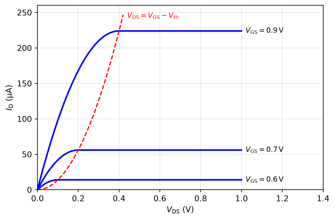
We see that \(g_\mathrm{m}\) is a linear function of the overdrive \(V_\mathrm{od}= V_\mathrm{GS}- V_\mathrm{th}\) (leading to a quadratic rise of the drain current), or a square-root function of \(I_\mathrm{D}\), or simply the drain current divided by half the overdrive voltage. Note that for a BJT \(g_\mathrm{m}= I_\mathrm{C} / V_\mathrm{T}\), so the MOSFET offers more degrees of freedom. Figure 9 shows the complete output characteristic including the boundary between triode and saturation.
2.2.5 Complementary MOS (CMOS)
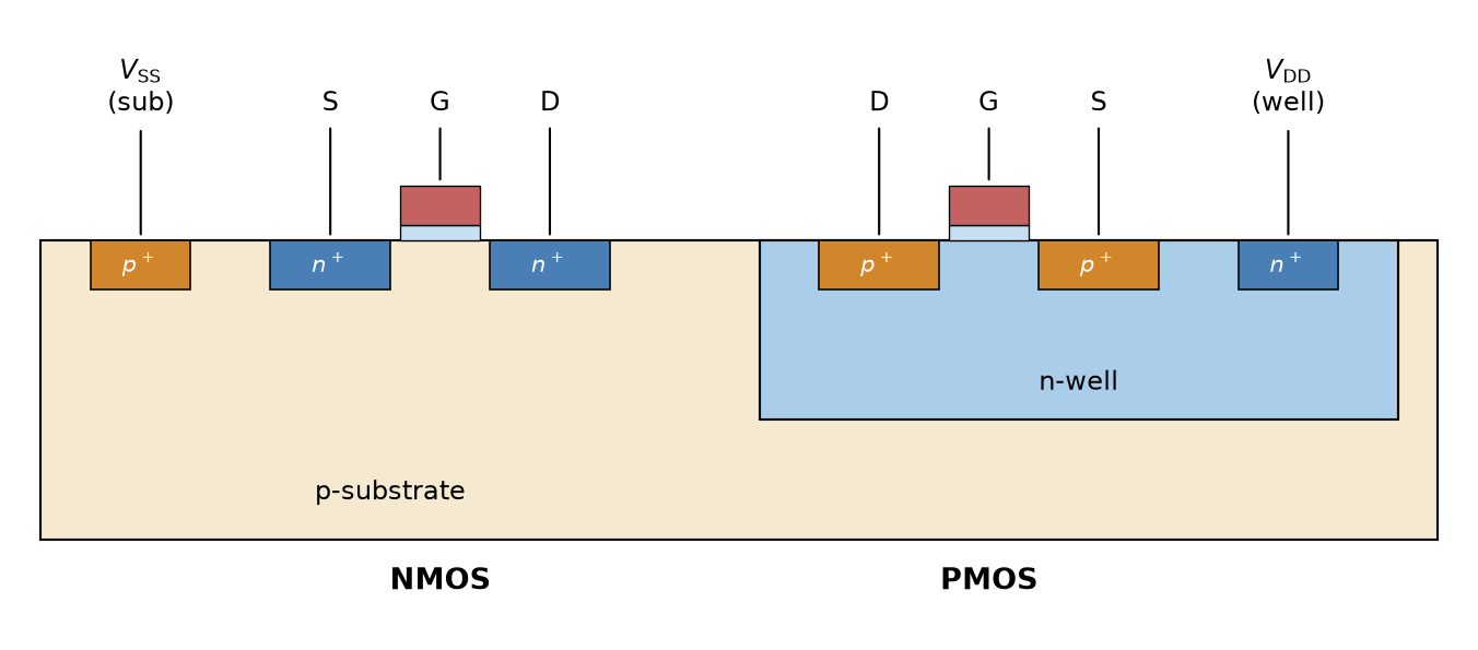
In CMOS technologies, both NMOS and PMOS devices are needed and fabricated on the same wafer, as shown in Figure 10. Usually, the PMOS is located in a local \(n\)-well, and this \(n\)-well is tied to the most positive supply voltage (\(V_\mathrm{DD}\)), while the \(p\)-substrate is tied to ground (\(V_\mathrm{SS}\)). The substrate contacts are realized with \(p^+\)-diffusions in the \(p\)-substrate (forming an ohmic contact), and the well contacts are realized with \(n^+\)-diffusions in the \(n\)-well.
For increased isolation (especially for analog applications), a triple-well (or “deep \(n\)-well,” DNW) option is sometimes available; the NMOS is then located in a local \(p\)-well which is fully enclosed by an \(n\)-well and thus isolated from the common substrate.
In Figure 11, we see a simple CMOS inverter consisting of a PMOS and an NMOS transistor. The PMOS is connected to the positive supply voltage \(V_\mathrm{DD}\), while the NMOS is connected to ground \(V_\mathrm{SS}\). The gates of both transistors are tied together and form the input \(A\) of the inverter, while the drains are also tied together and form the output \(Y\). When the input is low, the PMOS is on and the NMOS is off, pulling the output high. Conversely, when the input is high, the PMOS is off and the NMOS is on, pulling the output low.
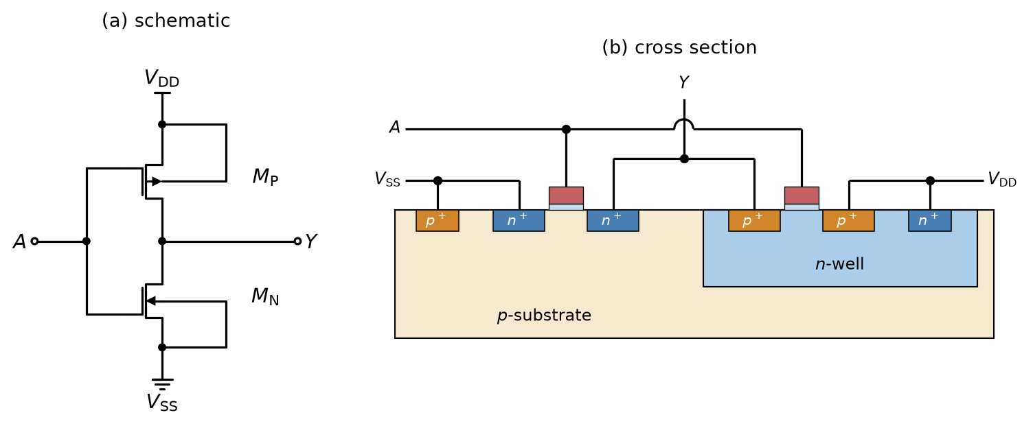
Note that in the CMOS technology shown in Figure 11, the bulk nodes of all the NMOS transistors are tied to the common substrate (\(V_\mathrm{SS}\)), while the bulk nodes of all the PMOS transistors are tied to the \(n\)-well (\(V_\mathrm{DD}\)). Since the \(n\)-wells are separated from the substrate (and can be separated between different PMOS devices), the bulk nodes of selected PMOS can be tied to different potentials than \(V_\mathrm{DD}\) (e.g., to the source of the PMOS), which is called body biasing. This can be used to adjust the threshold voltage of the PMOS transistors or to avoid the bulk effect (see Section 2.3.1).
2.3 Second-Order Effects in the MOSFET
The simple MOSFET model developed so far is only valid to first order for long-channel devices (\(L_\mathrm{min} > 1\,\mu\text{m}\)) under idealistic conditions. In the following, we discuss the most important second-order effects: the body effect, channel-length modulation, velocity saturation, mobility degradation with the vertical field, and subthreshold conduction.
2.3.1 Body Effect
In the derivation of Equation 7 we tied source, drain, and bulk together. Note that the inversion charge is a function of the bulk (substrate) potential \(V_\mathrm{B}\) versus the gate potential \(V_\mathrm{G}\), so when the source potential \(V_\mathrm{S}\) differs from \(V_\mathrm{B}\), the apparent \(V_\mathrm{th}\) becomes a function of \(V_\mathrm{SB}\), because inversion is reached at a surface potential of \(2 \Phi_\mathrm{B}+ V_\mathrm{SB}\) instead of \(2 \Phi_\mathrm{B}\).
This is the so-called body effect (or “back-gate effect”). The effective threshold voltage is given by (\(V_\mathrm{th0}\) is the threshold voltage with \(V_\mathrm{SB}= 0\))
\[ V_\mathrm{th}= V_\mathrm{th0} + \gamma \left( \sqrt{2 \Phi_\mathrm{B}+ V_\mathrm{SB}} - \sqrt{2 \Phi_\mathrm{B}} \right) \tag{15}\]
with the body-effect coefficient \(\gamma\) (the factor \(n\) will be introduced in Section 2.3.5)
\[ \gamma = \frac{\sqrt{2 q N_\mathrm{a}\varepsilon_\mathrm{si}}}{C'_\mathrm{ox}} = 2 (n - 1) \sqrt{2 \Phi_\mathrm{B}}. \tag{16}\]
Note that for \(n = 1\) (no body effect), \(\gamma = 0\) and thus \(V_\mathrm{th}= V_\mathrm{th0}\).
Note 2: Example Calculation of the Body Effect (NMOS)
Starting with the previously used values (\(N_\mathrm{a}= 3 \times 10^{18}\,\text{cm}^{-3}\), \(C'_\mathrm{ox}= 17.3\,\text{fF}/\mu\text{m}^2\), \(\Phi_\mathrm{B}= 0.50\,\text{V}\)), we get
\[ \gamma = \frac{\sqrt{2 q N_\mathrm{a}\varepsilon_\mathrm{si}}}{C'_\mathrm{ox}} = 0.58\,\text{V}^{1/2} \]
Let us consider the originally calculated \(V_\mathrm{th0} = 0.53\,\text{V}\) and assume the bulk is tied to \(V_\mathrm{SS}= V_\mathrm{B} = 0\,\text{V}\) while the source sits at \(V_\mathrm{S} = 0.5\,\text{V}\) (so \(V_\mathrm{SB}= 0.5\,\text{V}\)). Using Equation 15:
\[ V_\mathrm{th}= 0.53 + 0.58 \left( \sqrt{2 \cdot 0.50 + 0.5} - \sqrt{2 \cdot 0.50} \right) = 0.66\,\text{V} \]
In this case, the threshold voltage has been increased by 130 mV. Conversely, by tying the bulk to a higher potential than the source, the threshold voltage can also be decreased, but beware of the risk of forward-biasing the source-bulk pn-junction (see Figure 10)!
2.3.2 Channel-Length Modulation
In the derivation of the saturation current (Equation 13), we assumed that the channel is pinched off exactly at the drain when \(V_\mathrm{DS}= V_\mathrm{GS}- V_\mathrm{th}\). When \(V_\mathrm{DS}\) is increased further, this pinch-off point moves away from the drain towards the source. This can be viewed as an effective channel-length reduction, \(L_\mathrm{eff} = f(V_\mathrm{DS}) < L\), and we have to use \(L_\mathrm{eff}\) instead of \(L\) in Equation 13. Avoiding a direct calculation of \(L_\mathrm{eff}\), it is common to set \(1/L_\mathrm{eff} \approx (1 + \Delta L / L)/L\) with \(\Delta L/L = \lambda V_\mathrm{DS}\), so that
\[ I_\mathrm{D}= \frac{1}{2} \mu_\mathrm{n}C'_\mathrm{ox}\frac{W}{L} ( V_\mathrm{GS}- V_\mathrm{th})^2 (1 + \lambda V_\mathrm{DS}) \tag{17}\]
This so-called channel-length modulation leads to a reduced output impedance of the MOSFET, i.e., a nonzero output conductance (ideally, \(\lambda = 0\) and thus \(g_\mathrm{ds}= 0\)):
\[ g_\mathrm{ds}= \frac{\partial I_\mathrm{D}}{\partial V_\mathrm{DS}} = I_\mathrm{D}\rvert_{\lambda = 0} \cdot \lambda \tag{18}\]
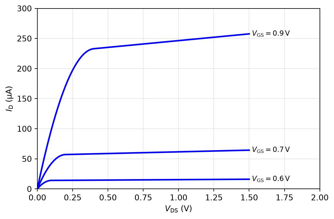
Since \(\lambda \propto 1/L\), the output resistance can be improved by increasing \(L\) beyond the minimum length, which is usually done when using the MOSFET as a current source. By scaling \(W\) along with \(L\), the aspect ratio can be kept constant. Figure 12 shows the output characteristic including channel-length modulation; note the finite slope of the curves in saturation.
2.3.3 Velocity Saturation
In the derivation of Equation 9, we assumed that the velocity of the carriers in the channel is given by \(v = \mu_\mathrm{n}E_\mathrm{DS}\). This is only true up to a certain speed limit of the carriers in silicon, which is around \(v_\mathrm{sat} = 10^7\,\text{cm/s}\). To take this velocity saturation into account, the following empirical model for the effective velocity can be used in the derivation:
\[ v_\mathrm{eff} = \begin{cases} \dfrac{\mu_\mathrm{n}E_\mathrm{DS}}{1 + {E_\mathrm{DS}}/{E_\mathrm{sat}}} & \text{if } E_\mathrm{DS} \leq E_\mathrm{sat} = {2 v_\mathrm{sat}}/{\mu_\mathrm{n}} \\[1ex] v_\mathrm{sat} & \text{otherwise} \end{cases} \tag{19}\]
If the MOSFET enters the velocity-saturation regime, the square-law relation no longer holds, and the drain current is given by
\[ I_\mathrm{D}= v_\mathrm{sat} C'_\mathrm{ox}W (V_\mathrm{GS}- V_\mathrm{th}). \tag{20}\]
In velocity saturation, \(I_\mathrm{D}\) is not a quadratic but a linear function of the overdrive voltage, and the transconductance hence saturates at
\[ g_\mathrm{m,sat} = v_\mathrm{sat} C'_\mathrm{ox}W \tag{21}\]
This result means that increasing the drain current beyond the velocity-saturation point does not result in an increased \(g_\mathrm{m}\), which is usually not useful.
In sub-micron technologies, it is relatively easy to reach velocity saturation: with \(\mu_\mathrm{n}= 280\,\text{cm}^2/(\text{V}\cdot\text{s})\), the resulting critical field is \(E_\mathrm{sat} = 7.1\,\text{V}/\mu\text{m}\), which is reached in a 0.13 µm CMOS technology at an overdrive of \(V_\mathrm{od}\approx 0.9\,\text{V}\)—achievable with a supply voltage of \(V_\mathrm{DD}= 1.5\,\text{V}\) and \(V_\mathrm{th}= 0.5\,\text{V}\)! Note that the stated \(\mu_\mathrm{n}\) is considerably lower than the mobility of pure silicon, because doping reduces mobility—yet another trade-off.1
2.3.4 Mobility Degradation with Vertical Field
With high \(V_\mathrm{GS}\), the channel is confined to a narrow region at the surface, leading to more carrier scattering and thus lower mobility (remember that at the SiO\(_2\)-silicon interface, scattering is more pronounced). We can model this effect empirically by setting
\[ \mu_\mathrm{n,eff} = \frac{\mu_\mathrm{n}}{1 + \Theta (V_\mathrm{GS}- V_\mathrm{th})} \tag{22}\]
and using this \(\mu_\mathrm{n,eff}\) instead of \(\mu_\mathrm{n}\) in the saturation current (Equation 13):
\[ I_\mathrm{D}= \frac{1}{2} \frac{\mu_\mathrm{n}C'_\mathrm{ox}}{1 + \Theta V_\mathrm{od}} \frac{W}{L} V_\mathrm{od}^2 \approx \frac{1}{2} \mu_\mathrm{n}C'_\mathrm{ox}\frac{W}{L} ( V_\mathrm{od}^2 - \Theta V_\mathrm{od}^3 ) \tag{23}\]
This introduces a cubic nonlinearity into an otherwise quadratic relationship, which can be relevant for precision analog and high-frequency circuits, with \(\Theta \approx (10^{-9}\,\text{m/V}) / t_\mathrm{ox}= 0.5\,\text{V}^{-1}\) for \(t_\mathrm{ox}= 2\,\text{nm}\).
2.3.5 Subthreshold Conduction
In the derivation of Equation 7, we assumed that inversion sets in abruptly when the surface potential reaches \(2 \Phi_\mathrm{B}\). However, even before reaching this level, there are already electrons present in the channel (for the NMOS; holes for the PMOS), which lead to conduction between drain and source even for \(V_\mathrm{GS}< V_\mathrm{th}\).
This mode of operation is called subthreshold conduction, and it leads to a leakage current based on diffusion when the MOSFET should be off. The drain current in this regime is described by
\[ I_\mathrm{D}= I_0 \frac{W}{L} e^{\frac{V_\mathrm{GS}}{n V_\mathrm{T}}} \left( 1 - e^{-\frac{V_\mathrm{DS}}{V_\mathrm{T}}} \right) = \mu_\mathrm{n}C'_\mathrm{ox}\frac{W}{L} \, 2 n V_\mathrm{T}^2 \, e^{\frac{V_\mathrm{GS}- V_\mathrm{th}}{n V_\mathrm{T}}} \left( 1 - e^{-\frac{V_\mathrm{DS}}{V_\mathrm{T}}} \right). \tag{24}\]
The nonideality factor (or slope factor) \(n\) is defined by (see Equation 16)
\[ n = 1 + \frac{C'_\mathrm{dep}}{C'_\mathrm{ox}} \tag{25}\]
and is on the order of 1 (perfect MOSFET) to 2 (pretty bad). Using the values of \(C'_\mathrm{ox}\) and \(C'_\mathrm{dep}\) from the previous examples, we get \(n = 1.29\). \(V_\mathrm{T}= k T / q\) is the well-known thermal voltage of \(25.8\,\text{mV}\) at \(300\,\text{K}\), and
\[ I_0 = \mu_\mathrm{n}C'_\mathrm{ox}\, 2 n V_\mathrm{T}^2 \, e^{-\frac{V_\mathrm{th}}{n V_\mathrm{T}}}. \]
Note that the depletion capacitance \(C'_\mathrm{dep}\) is given by Equation 3 evaluated at \(\Phi_\mathrm{S}= 2\Phi_\mathrm{B}\):
\[ C'_\mathrm{dep}= \sqrt{\frac{q N_\mathrm{a}\varepsilon_\mathrm{si}}{2 \cdot 2 \Phi_\mathrm{B}}} \]
The inversion condition used in the derivation of the threshold voltage in Equation 7 is the point where the electron concentration at the surface equals the bulk doping concentration \(N_\mathrm{a}\)—but even before this condition is met, there are electrons in the channel. Another way to look at this is that the surface potential effectively forward-biases the channel-source junction (since the channel region is \(p\)-type and the source is \(n^+\)), which can be seen in the plot of \(\Phi_\mathrm{S}\) in Figure 7. When the forward bias of this junction is gradually increased, electrons are injected into the channel area (similar to a BJT), moving across the channel by diffusion, and collected by the drain. At the point where the channel switches from \(p\)- to \(n\)-type due to inversion, this “diode” approaches an ohmic connection linking drain and source.
Although this weak inversion mode of the MOSFET is generally unwanted in digital circuits (as it leads to leakage currents), it is very useful for low-power analog (and digital) operation. Assuming \(V_\mathrm{DS}> 4 V_\mathrm{T}\approx 100\,\text{mV}\), then
\[ I_\mathrm{D}\approx I_0 \frac{W}{L} e^{\frac{V_\mathrm{GS}}{n V_\mathrm{T}}} \]
and the resulting transconductance is
\[ g_\mathrm{m}= \frac{\partial I_\mathrm{D}}{\partial V_\mathrm{GS}} = \frac{I_\mathrm{D}}{n V_\mathrm{T}} \tag{26}\]
This transconductance in weak inversion is similar to that of a BJT, except for the reduction by the factor \(n\)!
2.3.6 MOSFET I/V Characteristic Including the Body Effect
In the earlier derivation of the square law (Equation 10), we made a deliberate error: when the channel potential \(V_\mathrm{cs}\) departs from \(V_\mathrm{S}\) towards \(V_\mathrm{D}\), we need to take the body effect along the channel into account by using \(n V_\mathrm{cs}\) instead of \(V_\mathrm{cs}\), so \(Q'_\mathrm{inv}(x) = C'_\mathrm{ox}(V_\mathrm{GS}- n V_\mathrm{cs} - V_\mathrm{th})\). The corrected derivation is then
\[ \int_{0}^{L} I_\mathrm{D}\, dx = \mu_\mathrm{n}C'_\mathrm{ox}W \int_{0}^{V_\mathrm{DS}} ( V_\mathrm{GS}- n V_\mathrm{cs} - V_\mathrm{th}) \, dV_\mathrm{cs} \]
resulting in
\[ I_\mathrm{D}= \mu_\mathrm{n}C'_\mathrm{ox}\frac{W}{L} \left[ ( V_\mathrm{GS}- V_\mathrm{th}) V_\mathrm{DS}- \frac{n}{2} V_\mathrm{DS}^2 \right] \tag{27}\]
In the deep-triode region, there is no difference from the previous result, as the term \(n V_\mathrm{DS}^2 / 2\) vanishes for small \(V_\mathrm{DS}\). The saturation voltage is now \(V_\mathrm{DS,sat} = (V_\mathrm{GS}- V_\mathrm{th}) / n\), and the drain current in saturation becomes (compare to Equation 13)
\[ I_\mathrm{D}= I_\mathrm{DS,sat} = \frac{1}{2 n} \mu_\mathrm{n}C'_\mathrm{ox}\frac{W}{L} (V_\mathrm{GS}- V_\mathrm{th})^2. \tag{28}\]
The corrected expressions for the transconductance are
\[ g_\mathrm{m}= \mu_\mathrm{n}C'_\mathrm{ox}\frac{W}{L} \frac{V_\mathrm{GS}- V_\mathrm{th}}{n} = \sqrt{\frac{2}{n} \mu_\mathrm{n}C'_\mathrm{ox}\frac{W}{L} I_\mathrm{D}} = \frac{2 I_\mathrm{D}}{V_\mathrm{GS}- V_\mathrm{th}}. \tag{29}\]
2.4 MOSFET AC Operation
So far, we have only considered the dc operation of the MOSFET, but the physical construction of the transistor leads to unwanted capacitances and resistances, which need to be accounted for in dynamic operation. The most important capacitive elements are:
- The oxide capacitance between the gate and the channel, \(C_\mathrm{gg}= C'_\mathrm{ox}W L\).
- The gate-drain and gate-source overlap capacitances \(C_\mathrm{ov} = C'_\mathrm{ov} W\).
- The junction capacitance between drain/source and substrate, \(C_\mathrm{j} = C_\mathrm{j0} / (1 + V_\mathrm{DB | SB} / \Phi_\mathrm{B})^m\) with \(m \approx 0.3 \ldots 0.4\). \(C_\mathrm{j0}\) is defined by the area and perimeter of the drain/source regions.
- The depletion capacitance between the channel (the inversion layer) and the substrate, \(C_\mathrm{dep} = C'_\mathrm{dep}W L\).
To identify the dominant capacitive elements between gate-source (\(C_\mathrm{GS}\)) and gate-drain (\(C_\mathrm{GD}\)), we need to distinguish between the triode and the saturation region, see Table 2.
| Operating region | \(C_\mathrm{GS}\) | \(C_\mathrm{GD}\) |
|---|---|---|
| Triode | \(\frac{1}{2} C_\mathrm{gg}+ C_\mathrm{ov}\) | \(\frac{1}{2} C_\mathrm{gg}+ C_\mathrm{ov}\) |
| Saturation | \(\frac{2}{3} C_\mathrm{gg}+ C_\mathrm{ov}\) | \(C_\mathrm{ov}\) |
In addition to these capacitances, the resistance of the gate connection is usually dominant among the parasitic resistances. The end-to-end resistance of the gate stripe is \(R_\square \cdot W / L\) (with the sheet resistance \(R_\square\) set by the gate material). Due to the distributed nature of the gate along the width of the transistor, a reasonable lumped model for a single-sided gate contact is
\[ R_\mathrm{G} = \frac{1}{3} R_\square \frac{W}{L} \tag{30}\]
Using a double-sided gate contact, the effective gate resistance is reduced to
\[ R_\mathrm{G} = \left( \frac{1}{3} R_\square \frac{W}{2 \cdot L} \right) \parallel \left( \frac{1}{3} R_\square \frac{W}{2 \cdot L} \right) = \frac{1}{12} R_\square \frac{W}{L} \tag{31}\]
The impact of \(R_\mathrm{G}\) on performance can be further minimized by constructing a large transistor out of \(m\) smaller transistors connected in parallel (“fingers”). If the total width is \(W = m W'\) (with each finger having width \(W'\)), the gates of all unit transistors are connected in parallel, and the effective single-sided gate resistance becomes
\[ R_\mathrm{G,eff} = \frac{R'_\mathrm{G}}{m} = \frac{\frac{1}{3} R_\square \frac{W}{m \cdot L}}{m} = \frac{1}{m^2} R_\mathrm{G} \tag{32}\]
A typical analog/RF layout therefore splits a wide transistor into several fingers of limited length (a few µm), uses double-sided gate contacts, and surrounds the device with a closed well-contact ring; the multi-finger layout technique is discussed in detail in Section 4.5.
2.5 MOSFET Small-Signal Model
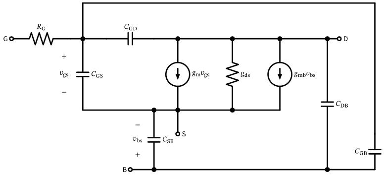
The complete small-signal model of a MOSFET in saturation is shown in Figure 13. The transconductance \(g_\mathrm{m}\) is modeled by a voltage-controlled current source, as is the body effect, which contributes a back-gate transconductance
\[ g_\mathrm{mb}= g_\mathrm{m}\frac{\gamma}{2 \sqrt{2 \Phi_\mathrm{B}+ V_\mathrm{SB}}}. \]
2.5.1 High-Frequency Operation
For high-frequency operation, the definition of the transit frequency \(f_\mathrm{T}\) is useful; this is the frequency where the magnitude of the current gain \(|I_\mathrm{ds}| / |I_\mathrm{gs}|\) falls to one. The ac drain current can be calculated based on the small-signal model:
\[ I_\mathrm{ds} (j \omega)= I_\mathrm{gs}(j \omega) \frac{g_\mathrm{m}- j \omega C_\mathrm{GD}}{j \omega (C_\mathrm{GS}+ C_\mathrm{GD})} \]
The transit frequency is thus (extrapolating the low-frequency transfer function)
\[ \omega_\mathrm{T} = 2 \pi f_\mathrm{T}\approx \frac{g_\mathrm{m}}{C_\mathrm{GS}+ C_\mathrm{GD}} \approx \frac{g_\mathrm{m}}{C_\mathrm{GG}} \approx \frac{3}{2 n} \frac{\mu}{L^2} (V_\mathrm{GS}- V_\mathrm{th}). \tag{33}\]
In addition, the maximum oscillation frequency \(f_\mathrm{max}\) is a useful metric; it is the frequency where the maximum available power gain drops to one (\(\text{MAG} = 0\,\text{dB}\)):
\[ f_\mathrm{max} \approx \sqrt{\frac{f_\mathrm{T}}{8 \pi R_\mathrm{G} C_\mathrm{GD}}} \tag{34}\]
2.5.2 Simplified Small-Signal Models
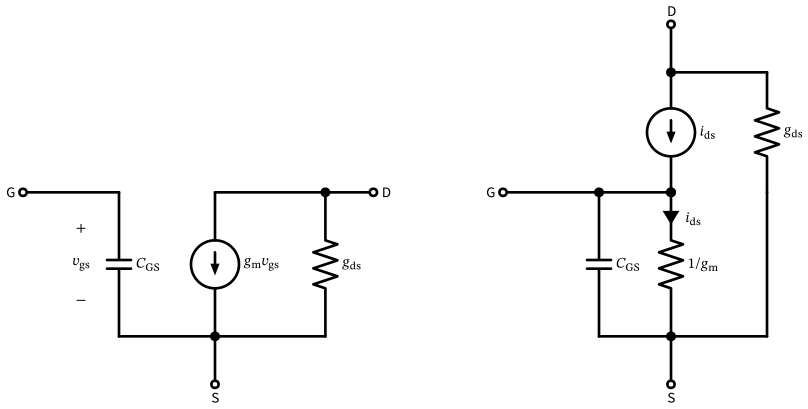
In most cases, a simplified model is sufficient for hand calculations. Neglecting most model elements, the two models shown in Figure 14 can be used in the saturation region. The left π-model is usually better suited for circuits with the signal input at the gate (like in a common-source or common-drain amplifier), whereas the right \(\tau\)-model is advantageous when the input is at the source (like in a common-gate amplifier).
2.6 MOSFET Scaling
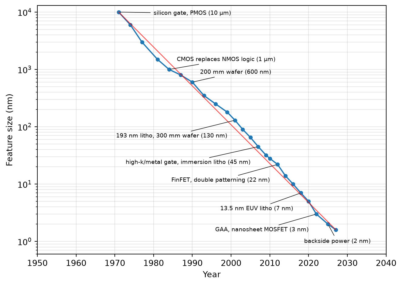
Making MOSFETs smaller has benefits for power, performance, and area (PPA). Traditionally, every 2–3 years a scaled (= smaller) CMOS technology node has been introduced. In Figure 15, the technology nodes are plotted versus their year of first volume production; note the logarithmic axis!
In the beginning, the node name stated the minimum feature size of the given technology, which is usually the minimum gate length (\(L_\mathrm{min}\)): in a 130 nm technology, \(L_\mathrm{min} = 130\,\text{nm}\). This holds well down to about the 90 nm node; from there on the printed gate length is already shorter than the node name (the 65 nm node used a physical gate length of roughly 35 nm), and from the 22/20 nm node onwards the technology name is merely a “label.” Since traditionally a scaling factor of \(\sqrt{2}\) has been used, the node names reflect this: 350 → 250 → 180 → 130 → 90 → 65 → 45 → 32/28 → 22/20 → 16/14 → 10 → 7 → 5 → 3 → 2 → 1.6 nm.
2.6.1 Scaling Theory
The ideal scaling theory follows three rules, formulated by R. Dennard in 1974 (Dennard et al. 1974), to generate the next CMOS technology node from the current one:
- Reduce all lateral and vertical dimensions by \(\alpha\) (\(\alpha = \sqrt{2}\) for classical scaling; the area of a MOSFET thus shrinks by \(\alpha^2 = 2\)).
- Reduce the threshold voltage \(V_\mathrm{th}\) and the supply voltage \(V_\mathrm{DD}\) by \(\alpha\).
- Increase all doping levels by \(\alpha\).
This scaling is called constant-field scaling. If we apply these rules, the MOSFET parameters in the shrunken technology (marked by \(^*\)) scale as follows. The drain saturation current is reduced by \(\alpha\):
\[ I^*_\mathrm{D} = \frac{1}{2} \mu_\mathrm{n}(\alpha C'_\mathrm{ox}) \frac{W / \alpha}{L / \alpha} \left( \frac{V_\mathrm{GS}}{\alpha} - \frac{V_\mathrm{th}}{\alpha} \right)^2 = \frac{1}{\alpha} I_\mathrm{D} \]
This is offset by the fact that the input capacitance is also reduced:
\[ C^*_\mathrm{gg} = \frac{W}{\alpha} \frac{L}{\alpha} (\alpha C'_\mathrm{ox}) = \frac{1}{\alpha} C_\mathrm{gg} \]
To estimate the scaling of the gate delay of logic gates built from scaled devices, we use the simple model \(T_\mathrm{d} \propto C_\mathrm{gg}V_\mathrm{DD}/ I_\mathrm{D}\), which relates the gate delay to the time it takes to charge or discharge the load capacitance of a driven gate between the supply rails. The scaled delay is
\[ T^*_\mathrm{d} = \frac{C_\mathrm{gg}/ \alpha}{I_\mathrm{D}/ \alpha} \frac{V_\mathrm{DD}}{\alpha} = \frac{1}{\alpha} T_\mathrm{d} \]
The speed of digital circuits thus benefits from scaling, as the gate delay shrinks in each new technology node! Using a simple model for the dynamic power consumption of CMOS logic, \(P_\mathrm{dyn} = f_\mathrm{clk} C_\mathrm{dyn} V_\mathrm{DD}^2\) (where \(f_\mathrm{clk}\) is the clock frequency and \(C_\mathrm{dyn} \propto C_\mathrm{gg}\) is the total switched capacitance), we see that
\[ P^*_\mathrm{dyn} = f_\mathrm{clk} \frac{C_\mathrm{dyn}}{\alpha} \left( \frac{V_\mathrm{DD}}{\alpha} \right)^2 = \frac{1}{\alpha^3} P_\mathrm{dyn} \]
so the dynamic power consumption of a scaled logic circuit benefits dramatically. Note that the power per function, clocked at the same frequency, scales by \(\alpha^{-3}\)—but since we can also increase the clock frequency by \(\alpha\), and can integrate \(\alpha^2\) more gates per area, the total power consumption would stay constant if we fully exploited the scaling benefit. To improve power, performance, and area (PPA) simultaneously, a trade-off has to be found.
2.6.2 Analog Scaling
While there is a clear scaling benefit for digital circuits, the benefits for analog circuits are less clear. Generally, the reduction of \(V_\mathrm{DD}\) is a drawback, since it likely reduces the dynamic range when processing voltage signals. The transconductance scales like
\[ g^*_\mathrm{m} = \mu_\mathrm{n}(\alpha C'_\mathrm{ox}) \frac{W / \alpha}{L / \alpha} \frac{V_\mathrm{GS}- V_\mathrm{th}}{\alpha} = g_\mathrm{m} \]
so it seems to be scale-invariant. However, there is a benefit in device speed, as the transit frequency scales like
\[ f^*_\mathrm{T} = \frac{1}{2 \pi} \frac{g_\mathrm{m}}{C_\mathrm{gg}/ \alpha} = \alpha f_\mathrm{T} \]
so the speed of the MOSFET increases, opening the door to better analog and RF performance, albeit at lower supply voltages.
2.6.3 Scaling Summary
Table 3 summarizes the constant-field scaling factors derived above. Scaling equations fitted to real technology data from 180 nm down to 7 nm can be found in (Stillmaker and Baas 2017).
| Parameter | Symbol | Scaling factor |
|---|---|---|
| Gate length | \(L_\mathrm{min}\) | \(\alpha^{-1}\) |
| MOSFET area | \(W L\) | \(\alpha^{-2}\) |
| Gate oxide thickness | \(t_\mathrm{ox}\) | \(\alpha^{-1}\) |
| Substrate doping | \(N_\mathrm{a}\) | \(\alpha\) |
| Drain current in saturation | \(I_\mathrm{D}\) | \(\alpha^{-1}\) |
| Gate capacitance | \(C_\mathrm{GS}\) | \(\alpha^{-1}\) |
| Supply voltage | \(V_\mathrm{DD}\) | \(\alpha^{-1}\) |
| Threshold voltage | \(V_\mathrm{th}\) | \(\alpha^{-1}\) |
| Gate delay | \(T_\mathrm{d}\) | \(\alpha^{-1}\) |
| Clock frequency | \(f_\mathrm{clk}\) | \(\alpha\) |
| Dynamic power consumption per gate | \(P_\mathrm{dyn}\) | \(\alpha^{-3}\) |
2.6.4 Interconnect Scaling
As the MOSFETs get smaller, the metal wiring also needs to scale to finer dimensions. We assume that, along with the lateral dimensions, the metal thickness and the dielectric inter-metal insulation scale down as well. The resistance per length of a scaled metal wire (with thickness \(t\) and width \(w\)) scales as
\[ \frac{R^*}{l} = \rho \frac{1}{(t / \alpha) (w / \alpha)} = \alpha^2 \frac{R}{l} \]
so the wires get significantly more resistive! The wire-to-wire fringe capacitance per length for a minimum-width wire with minimum spacing \(s\) scales as
\[ \frac{C^*_\mathrm{f}}{l} = \varepsilon_\mathrm{ox}\frac{t / \alpha}{s / \alpha} = \frac{C_\mathrm{f}}{l} \]
and the vertical coupling capacitance per length (with insulator thickness \(h\)) scales as
\[ \frac{C^*_\mathrm{p}}{l} = \varepsilon_\mathrm{ox}\frac{w / \alpha}{h / \alpha} = \frac{C_\mathrm{p}}{l} \]
so both capacitance values are, to first order, invariant to scaling. The RC wire delay per squared length is thus
\[ \frac{T^*_\mathrm{wire}}{l^2} \propto \frac{R^*}{l} \left( \frac{C^*_\mathrm{f}}{l} + \frac{C^*_\mathrm{p}}{l} \right) = \alpha^2 \frac{T_\mathrm{wire}}{l^2} \]
For short routes, this increased relative delay is offset by the length scaling, so that
\[ T^*_\mathrm{wire} \propto \left( \frac{l}{\alpha} \right)^2 \frac{T^*_\mathrm{wire}}{l^2} = T_\mathrm{wire} \]
For long routes, however, the wire delay increases significantly. To cope with this delay, other solutions are needed: using multiple wiring levels (lower metals levels scaled for density, higher ones un-scaled for speed), or adapting the architecture, e.g., pipelining long-range data transfers.
2.7 MOSFET Short-Channel Effects
As the MOSFET gate length is scaled below \(1\,\mu\text{m}\), various imperfections kick in. We discuss subthreshold conduction and leakage, gate oxide leakage, and drain-induced barrier lowering (DIBL). Other effects, like random dopant fluctuation (RDF), poly depletion, or quantum-mechanical effects, are not covered here.
2.7.1 Subthreshold Leakage
Revisiting Equation 24 and neglecting the \(V_\mathrm{DS}\)-dependent term, we can re-formulate the subthreshold drain current as
\[ I_\mathrm{D}= 100\,\text{nA} \cdot \frac{W}{L} \, e^{\frac{V_\mathrm{GS}- V_\mathrm{th}}{n V_\mathrm{T}}} \tag{35}\]
Here, \(V_\mathrm{th}\) has been re-defined as the \(V_\mathrm{GS}\) at which \(I_\mathrm{D}= 100\,\text{nA} \cdot W / L\), which is a quite practical definition for leakage current discussions. The nonideality factor can also be written as
\[ n = 1 + \frac{C'_\mathrm{dep}}{C'_\mathrm{ox}} = 1 + \underbrace{\frac{\varepsilon_\mathrm{si}}{\varepsilon_\mathrm{ox}}}_{\approx 3} \frac{t_\mathrm{ox}}{W_\mathrm{dep}} \tag{36}\]
Using Equation 35, we see that the leakage current in the off-state (\(V_\mathrm{GS}= 0\)) is impacted by only two parameters (\(W/L\) is usually fixed by the circuit design):
\[ I_\mathrm{leak} = 100\,\text{nA} \cdot \frac{W}{L} \, e^{-\frac{V_\mathrm{th}}{n V_\mathrm{T}}} \tag{37}\]
- The threshold voltage \(V_\mathrm{th}\): a lower \(V_\mathrm{th}\) increases the overdrive when the MOSFET is turned on and thus reduces the gate delay, but it exponentially increases the leakage current.
- The nonideality factor \(n\) (ideally, \(n = 1\)).
2.7.2 Subthreshold Slope
To quantify the “turn-off” behavior of a MOSFET, the subthreshold slope \(S\) is defined, starting from Equation 35, and consisting of the two only parameters \(V_\mathrm{T}\) and \(n\):
\[ S = \left[ \frac{\partial (\log_{10} I_\mathrm{D})}{\partial V_\mathrm{GS}} \right]^{-1} = \frac{n V_\mathrm{T}}{\log_{10}(e)} = 2.3 \, n V_\mathrm{T} \tag{38}\]
The subthreshold slope expresses which change of \(V_\mathrm{GS}\) lowers (or increases) the drain current by a factor of ten. Ideally, \(S\) should be as small as possible, meaning that the MOSFET can be turned off rapidly with a small change of \(V_\mathrm{GS}\):
- The lower bound is \(S = 2.3 V_\mathrm{T}= 59.4\,\text{mV/dec}\) at \(300\,\text{K}\).
- Using \(n = 1.29\) from the previous example, \(S = 76.6\,\text{mV/dec}\), which is a good value; \(S\) for bulk CMOS is in the range of 80 to 120 mV/dec.
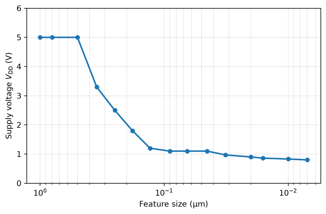
The impact of the subthreshold slope essentially stopped the scaling of \(V_\mathrm{DD}\) and \(V_\mathrm{th}\), as the leakage current would otherwise become impractically large. This issue is exacerbated by the temperature dependence of the threshold voltage of \(\approx -1\,\text{mV/K}\) and its process variation on the order of \(\pm 50\,\text{mV}\). A threshold-voltage shift of a hundred millivolts may not sound like much, but it enters the leakage exponentially and thus has a drastic impact! Figure 16 shows how the supply voltage stopped scaling at around 0.8 V.
2.7.3 Gate Oxide Leakage
As can be seen in Equation 36, to minimize \(n\) (and thus the subthreshold slope), and also to increase the drain current in saturation, \(C'_\mathrm{ox}\) needs to be maximized. This has driven the scaling down of the gate oxide thickness, as discussed in the scaling rules. Over the years, the oxide thickness has been reduced from 300 nm to 1.2 nm, but severe issues appear once the oxide is only a few nanometers thick:
- The breakdown voltage of the oxide is reduced, mandating a low \(V_\mathrm{DD}\).
- The gate leakage current increases dramatically due to quantum-mechanical tunneling.
An alternative is needed to increase \(C'_\mathrm{ox}\) without further reducing \(t_\mathrm{ox}\): the introduction of alternative gate dielectrics with increased permittivity, the so-called high-k gate dielectrics. One suitable material is hafnium dioxide: while SiO2 has \(\varepsilon_\mathrm{r} = 3.9\), HfO2 offers \(\varepsilon_\mathrm{r} = 24\). However, there are potential manufacturing issues, like chemical reactions with the silicon substrate and the gate material, reliability concerns, and reduced surface mobility. Still, high-k dielectrics are now widely used in modern CMOS processes.
2.7.4 Drain-Induced Barrier Lowering (DIBL)
In scaled MOSFETs, there exists another parasitic effect that lowers \(V_\mathrm{th}\) as a function of \(L\), called drain-induced barrier lowering (DIBL). (Remember that lowering \(V_\mathrm{th}\) has an exponential effect on the leakage current!) This lowering of \(V_\mathrm{th}\) with decreasing \(L\) is also called the short-channel effect (SCE). Note that there is also a reverse short-channel effect (RSCE), which increases \(V_\mathrm{th}\) with decreasing \(L\), caused by halo implants around drain and source in modern CMOS processes. Effectively, \(V_\mathrm{th}= f(L)\) can be a wild function of the MOSFET length, so devices will only match if constructed with the same \(L\)! Note that \(V_\mathrm{th}\) also depends on \(V_\mathrm{DS}\) due to DIBL, and on device \(W\), as well as temperature, and other second-order effects, so ultimately \(V_\mathrm{th}= f(L, W, V_\mathrm{DS}, T)\)!
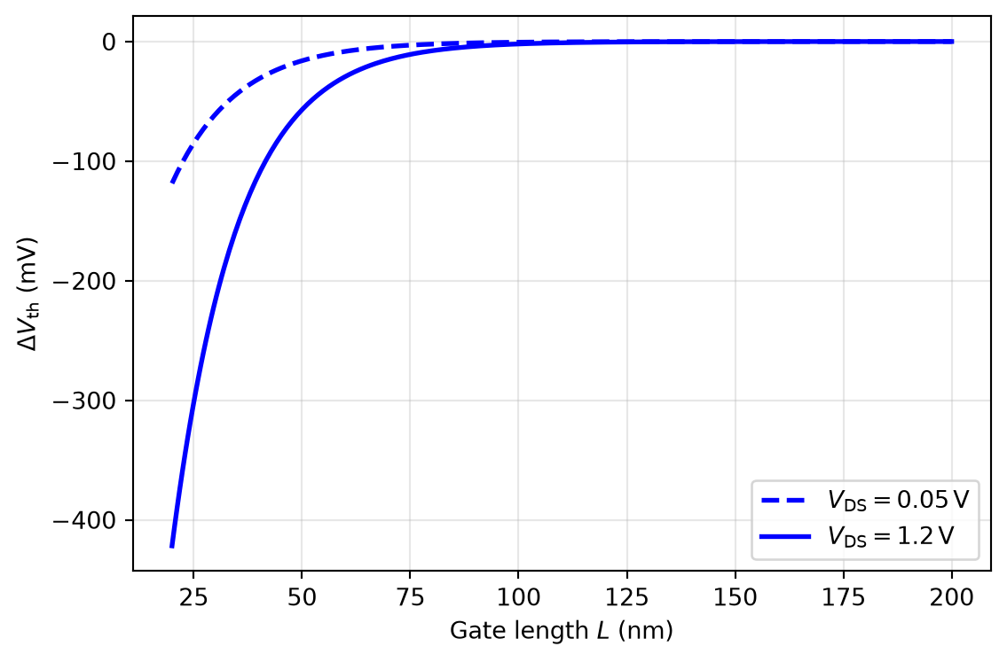
The impact of \(L\) and \(V_\mathrm{DS}\) on \(V_\mathrm{th}\) can be modeled by
\[ \Delta V_\mathrm{th}= - (V_\mathrm{DS}+ 0.4\,\text{V}) \, e^{-L/l_\mathrm{d}} \tag{39}\]
and is illustrated in Figure 17. The DIBL characteristic length is \(l_\mathrm{d} \propto \sqrt[3]{t_\mathrm{ox}W_\mathrm{dep}X_\mathrm{j}}\). To reduce \(l_\mathrm{d}\), one or all of these parameters must be reduced:
- The oxide thickness \(t_\mathrm{ox}\), which has already been discussed in the context of gate leakage.
- The depletion width \(W_\mathrm{dep}\).
- The drain junction depth \(X_\mathrm{j}\).
Reducing the depletion width and the junction depth requires increasing \(N_\mathrm{a}\) (see Equation 2). However, increasing \(N_\mathrm{a}\) also increases \(V_\mathrm{th}\) (see Equation 7), which must be counteracted by increasing \(C'_\mathrm{ox}\)—but there are limits due to gate leakage and breakdown, as discussed before. In addition, increasing \(N_\mathrm{a}\) increases the subthreshold slope (see Equation 36) and lowers the mobility due to dopant scattering. So an alternative to ever-increasing substrate doping had to be found.
2.7.5 Solving DIBL: The Ultra-Thin-Body MOSFET
As scaling up \(N_\mathrm{a}\) to constrain the vertical dimensions has reached its limits, an alternative solution is to remove the silicon under the channel to physically constrain \(W_\mathrm{dep}\) and \(X_\mathrm{j}\). In the ultra-thin-body (UTB) MOSFET, the silicon channel is realized on top of a layer of SiO2, so the depletion and junction depths are limited to the silicon film thickness \(t_\mathrm{si} \leq L/4\). This is called silicon-on-insulator (SOI) technology; the structure is shown in Figure 18 (a). Additional advantages are:
- Since much less body doping \(N_\mathrm{a}\) is needed, the carrier mobility is higher.
- There is no (or only a small) body effect, since the body is floating and fully depleted.
- The drain/source-to-bulk capacitance is largely reduced and almost constant.
The disadvantage is the higher cost of the SOI wafers, as manufacturing the Si-SiO2-Si stack is expensive.
2.7.6 Solving DIBL: FinFET and Nanosheet
Another alternative is to tilt the silicon channel by 90°, so that it sticks out of the wafer like a “fin,” and to wrap the gate around this fin on three sides: the FinFET (or tri-gate MOSFET), shown in Figure 18 (b). FinFETs have a few important differences compared to bulk MOSFETs:
- The device width is quantized, with \(W = W_\mathrm{F} + 2 H_\mathrm{F}\) per fin (\(W_\mathrm{F}\) is the width and \(H_\mathrm{F}\) the height of the fin), so the circuit design style must be adapted (the design parameter is the number of fins \(N_\mathrm{F}\) instead of \(W\)).
- Drain and source are contacted at the ends of the fin, so the series resistances \(R_\mathrm{S}\) and \(R_\mathrm{D}\) are higher, degrading the transconductance due to series feedback: \(g_\mathrm{m,eff} = g_\mathrm{m}/ (1 + g_\mathrm{m}R_\mathrm{S})\).
- Since the subthreshold slope is improved (smaller), the leakage current is lower, which allows lowering \(V_\mathrm{th}\) and \(V_\mathrm{DD}\).
- DIBL and thus \(g_\mathrm{ds}\) are lower, so the MOSFET self-gain \(g_\mathrm{m}/ g_\mathrm{ds}\) is high.
- There is practically no body effect, and due to the low channel doping the mobility is high, leading to improved \(g_\mathrm{m}/I_\mathrm{D}\) and \(\mu_\mathrm{n}\approx \mu_\mathrm{p}\).
- The silicon fins are isolated and surrounded by SiO2, so self-heating of the fin can be an issue.
- The 3D structure increases the coupling capacitance \(C_\mathrm{ov}\).
- A drawback is that SRAM and digital standard cells often use minimum-size transistors, and for yield reasons a minimum-sized FinFET requires two fins—a strong constraint when, e.g., the PMOS needs to be sized differently from the NMOS (the next step up is three fins, a large quantization step).
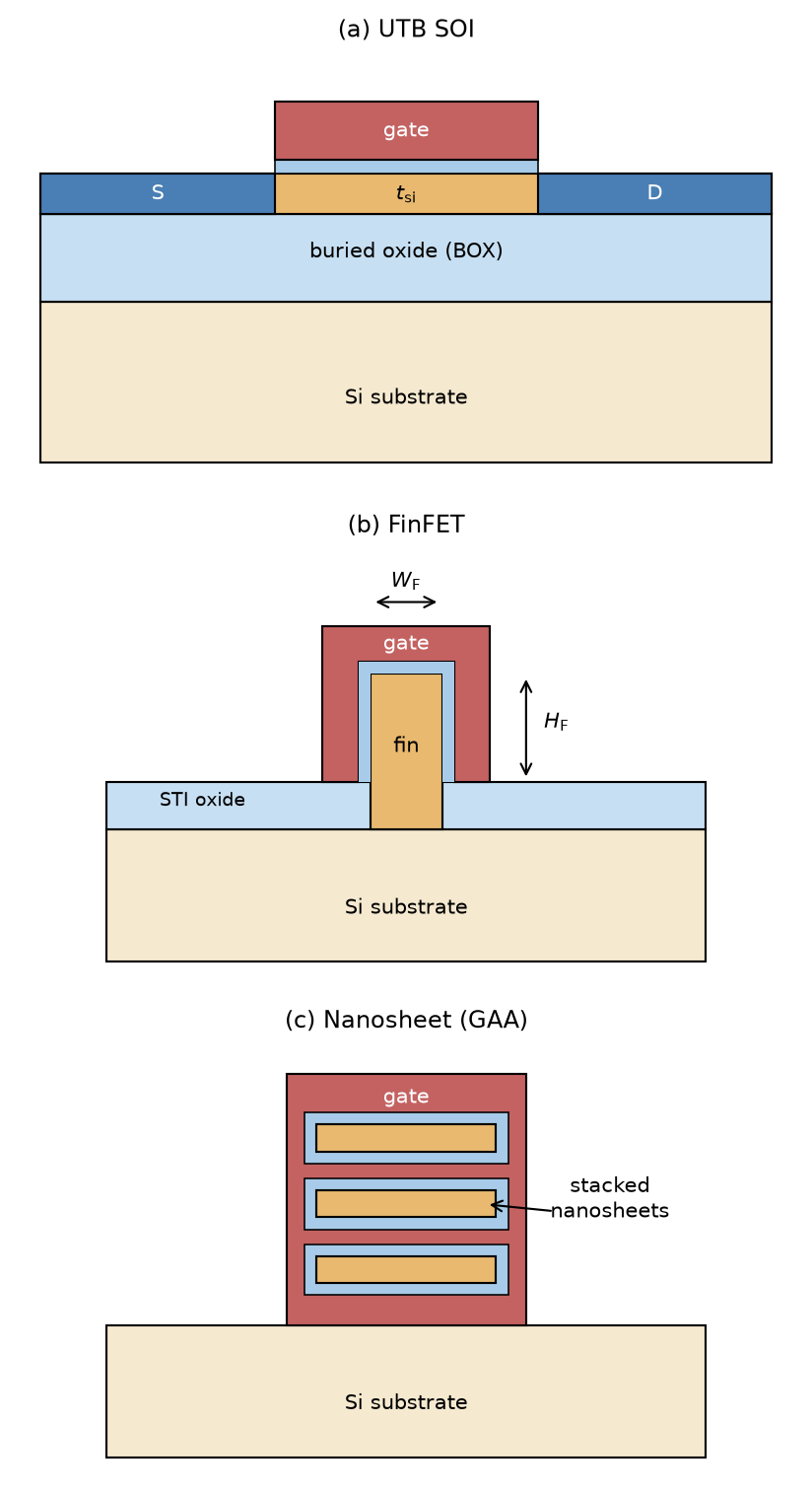
The evolution of the FinFET is the nanosheet MOSFET, first introduced at the 3 nm node (and used by all foundries at 2 nm) and shown in Figure 18 (c). One advantage is the even better electrostatic control of the gate over the channel, as the stacked channels are completely wrapped by the gate—hence also called gate-all-around (GAA) MOSFET. In addition, the stacked channels can be either \(n\)- or \(p\)-type (or mixed), and could even use different materials, like SiGe or GaAs, opening the door to 3D integration.
2.8 Simulated Characteristics in IHP SG13
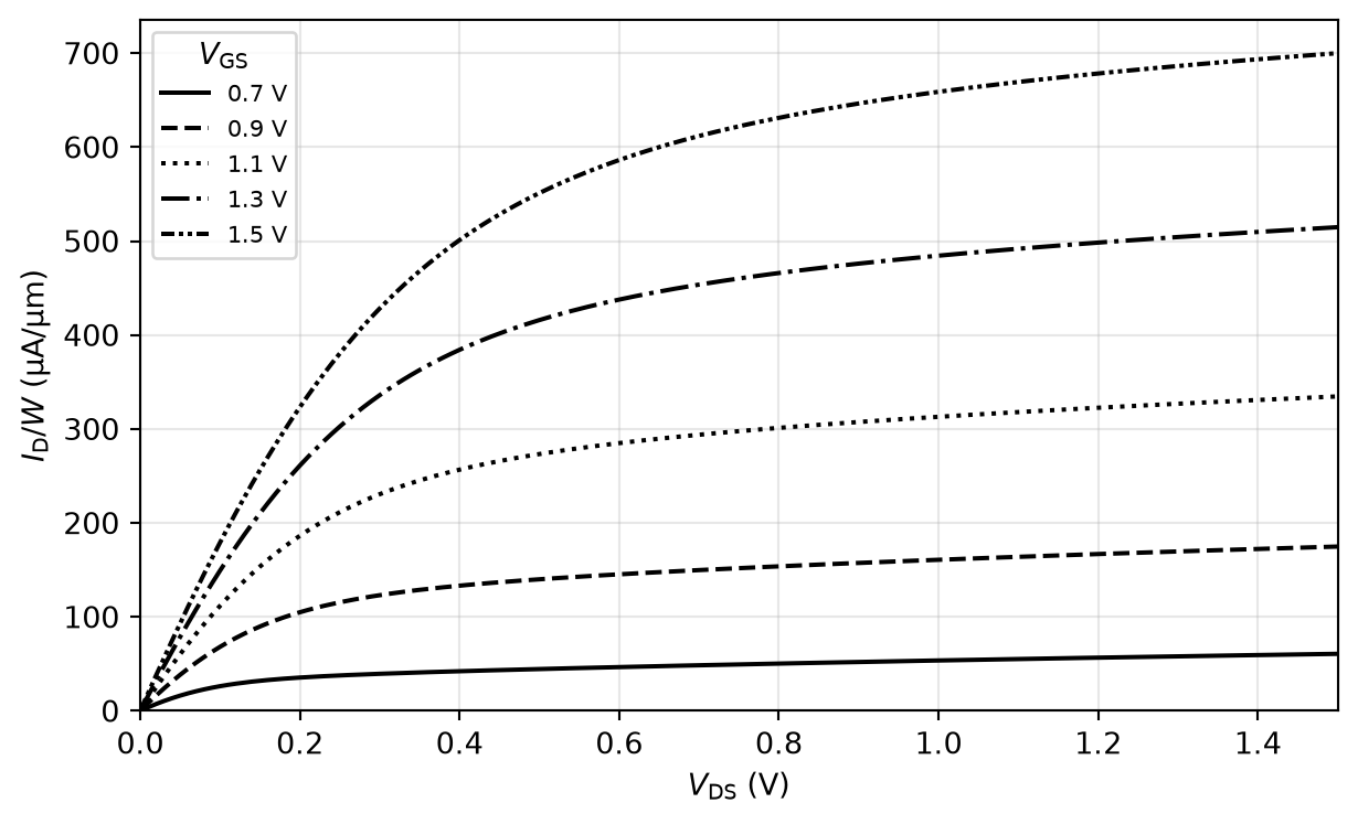
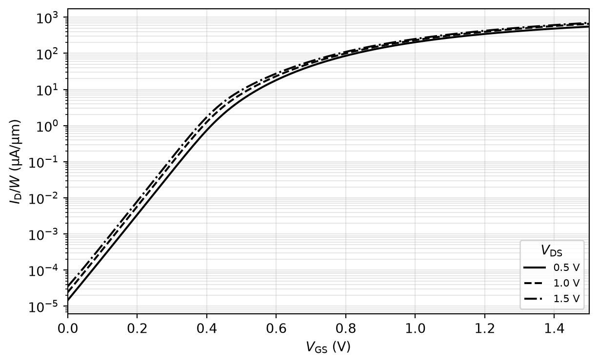
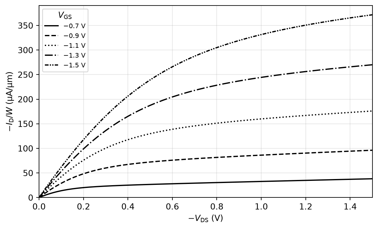
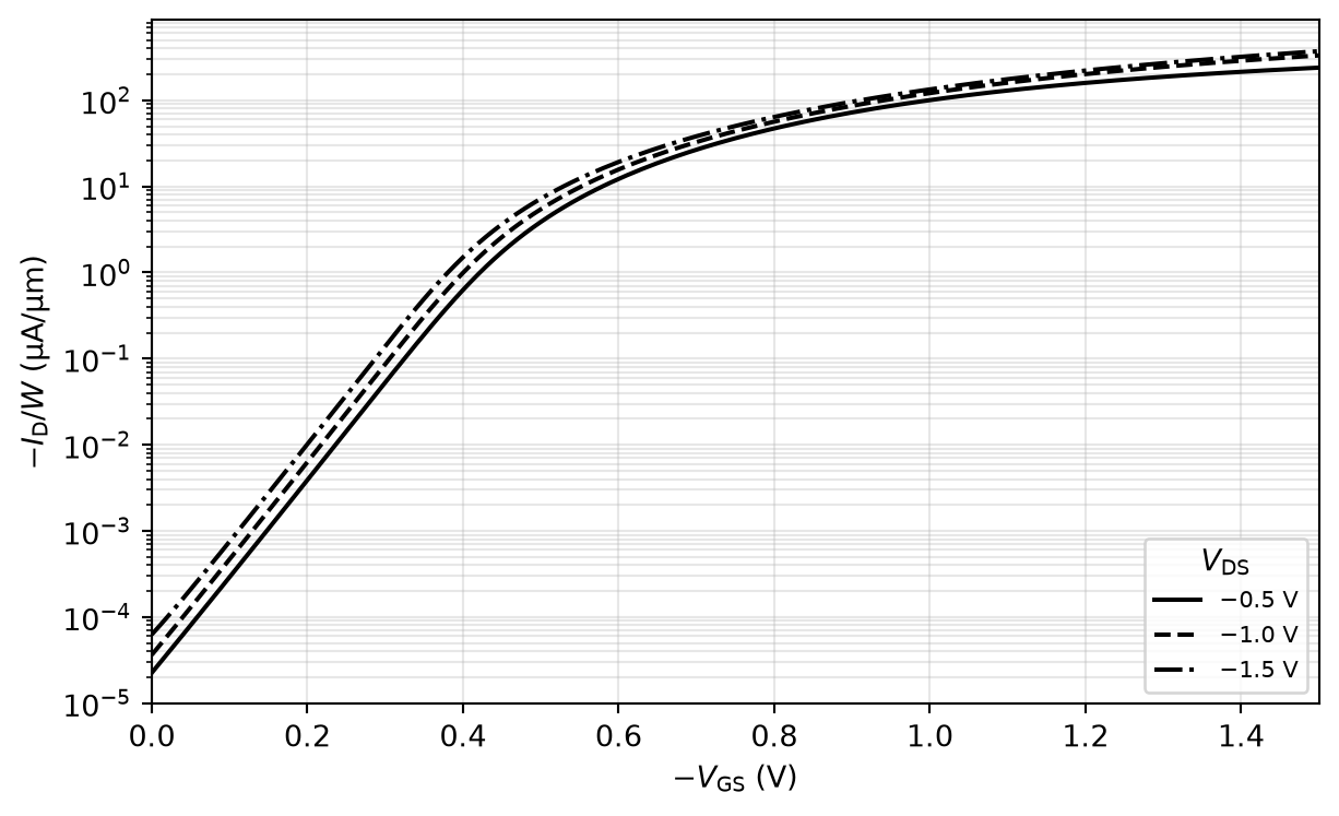
To connect the simple models we derived earlier to reality, Figure 19 to Figure 22 show simulated I/V characteristics of NMOS and PMOS devices (\(W = 1.3\,\mu\text{m}\), \(L = 0.13\,\mu\text{m}\), \(V_\mathrm{SB}= 0\)) in the IHP SG13 130 nm CMOS technology, using the foundry’s PSP models. The output characteristics show the triode and saturation regions including channel-length modulation, while the logarithmic transfer characteristics clearly show the exponential subthreshold region and the drain-current dependence on \(V_\mathrm{DS}\) caused by DIBL.
2.9 MOSFET Sizing
2.9.1 The \(g_\mathrm{m}/I_\mathrm{D}\) Method
When designing a circuit with MOSFETs, how should one select the parameters like \(I_\mathrm{D}\), \(V_\mathrm{GS}\), \(W\), and \(L\)? For digital designs, this is relatively straightforward: \(L\) is (usually) set to the minimum length, \(W\) is sized according to the driving requirements of the logic circuit, \(V_\mathrm{GS}\) swings between \(V_\mathrm{SS}\) and \(V_\mathrm{DD}\), and no static drain current flows. For analog, mixed-signal, and RF designs, the sizing question is more involved.
In the Analog Circuit Design course, the \(g_\mathrm{m}/I_\mathrm{D}\) method is used to find the proper sizing of a MOSFET depending on the circuit requirements. This method is the “go-to” method, as it uses numerical data found by evaluating the PDK models in a circuit simulator, and it describes the MOSFET correctly in all operating regions.
2.9.2 The Inversion-Coefficient Method
Despite the practical advantages of the \(g_\mathrm{m}/I_\mathrm{D}\) method, alternative approaches exist, and they can be helpful by providing relatively simple and unified analytical equations which are valid in all MOSFET operating regions. One such method is based on the inversion coefficient, which has been popularized as a design methodology by W. Sansen (Sansen 2015; Sansen 2006). Let us define a specific current
\[ I_\mathrm{S} = \mu C'_\mathrm{ox}\frac{W}{L} \cdot 2 n V_\mathrm{T}^2. \tag{40}\]
Then, the inversion coefficient \(\mathrm{IC}\) is defined as
\[ \mathrm{IC}= \frac{I_\mathrm{D}}{I_\mathrm{S}} = \left[ \ln \left( 1 + e^{\frac{V_\mathrm{GS}- V_\mathrm{th}}{2 n V_\mathrm{T}}} \right) \right]^2 \tag{41}\]
The beauty of this approach is that these equations work all the way from weak inversion (subthreshold operation, \(\mathrm{IC}< 0.1\)) through moderate inversion (\(\mathrm{IC}\approx 1\)) to strong inversion (\(\mathrm{IC}> 10\)). Based on the selected \(\mathrm{IC}\), the important device properties can be calculated. The drain current is
\[ I_\mathrm{D}= I_\mathrm{S} \cdot \mathrm{IC} \tag{42}\]
the transconductance is given by
\[ g_\mathrm{m}= \frac{I_\mathrm{D}}{n V_\mathrm{T}} \frac{1 - e^{-\sqrt{\mathrm{IC}}}}{\sqrt{\mathrm{IC}}} \tag{43}\]
and the speed of the MOSFET is
\[ f_\mathrm{T}= \frac{1}{2 \pi} \frac{3}{2} \frac{\mu}{L^2} V_\mathrm{T}\left( \sqrt{1 + 4 \, \mathrm{IC}} -1 \right) \tag{44}\]
Let us check the asymptotic behavior of these equations against the earlier results (see Table 4).
| Equation | \(V_\mathrm{GS}\ll V_\mathrm{th}\) (weak inversion) | \(V_\mathrm{GS}\gg V_\mathrm{th}\) (strong inversion) |
|---|---|---|
| Equation 41 | \(\mathrm{IC}= e^{\frac{V_\mathrm{GS}- V_\mathrm{th}}{n V_\mathrm{T}}}\) | \(\mathrm{IC}= \left( \frac{V_\mathrm{GS}- V_\mathrm{th}}{2 n V_\mathrm{T}} \right)^2\) |
| Equation 42 | \(I_\mathrm{D}= \mu C'_\mathrm{ox}\frac{W}{L} 2 n V_\mathrm{T}^2 e^{\frac{V_\mathrm{GS}- V_\mathrm{th}}{n V_\mathrm{T}}}\) | \(I_\mathrm{D}= \frac{1}{2 n} \mu C'_\mathrm{ox}\frac{W}{L} \left( V_\mathrm{GS}- V_\mathrm{th}\right)^2\) |
| Equation 43 | \(g_\mathrm{m}= \frac{I_\mathrm{D}}{n V_\mathrm{T}}\) | \(g_\mathrm{m}= \frac{2 I_\mathrm{D}}{V_\mathrm{GS}- V_\mathrm{th}}\) |
| Equation 44 | \(f_\mathrm{T}= \frac{1}{2 \pi} \frac{3}{2} \frac{\mu}{L^2} 2 V_\mathrm{T}e^{\frac{V_\mathrm{GS}- V_\mathrm{th}}{n V_\mathrm{T}}}\) | \(f_\mathrm{T}= \frac{1}{2 \pi} \frac{3}{2 n} \frac{\mu}{L^2} \left( V_\mathrm{GS}- V_\mathrm{th}\right)\) |
The asymptotes match the subthreshold model (Equation 24) and the corrected square-law model (Equation 28), respectively.
Plotting Equation 43 and Equation 44 versus \(\mathrm{IC}\), as done in Figure 23, reveals the classical trade-off between \(g_\mathrm{m}\)-efficiency (\(g_\mathrm{m}/I_\mathrm{D}\)) and speed (\(f_\mathrm{T}\)). Note that velocity saturation is not represented in this simple model, so \(f_\mathrm{T}\) does not saturate at high \(\mathrm{IC}\) in the plot.
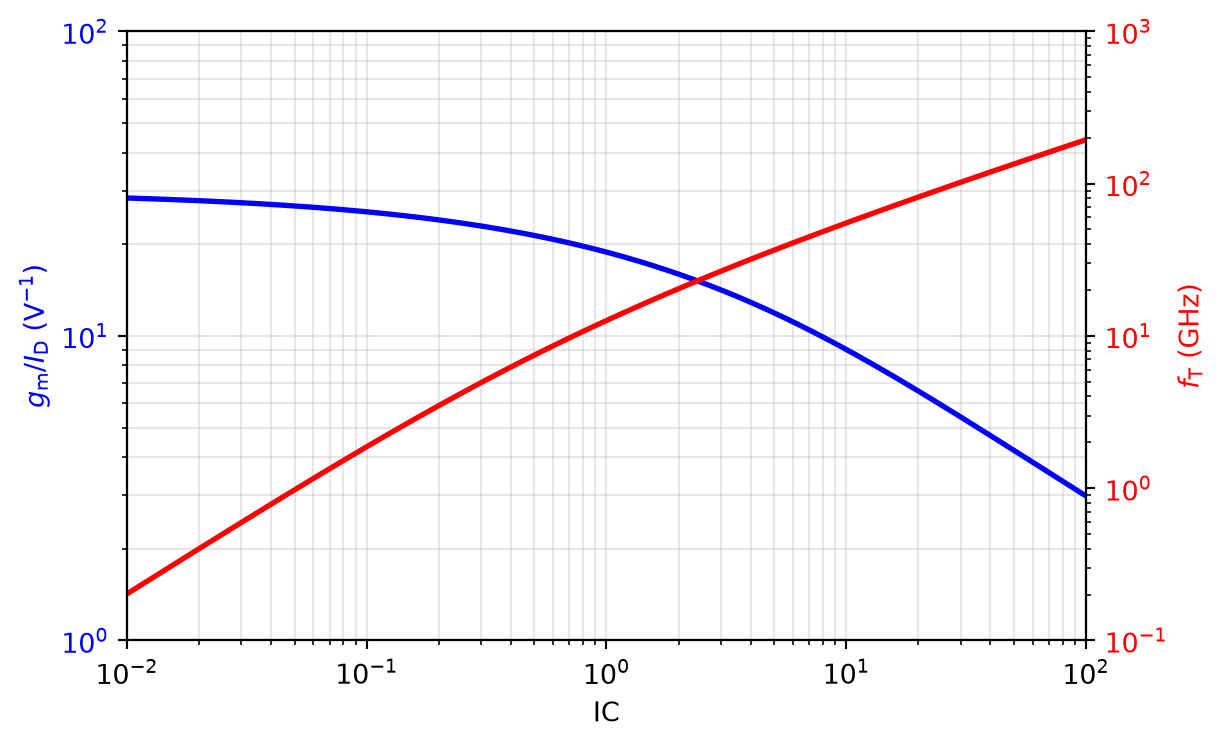
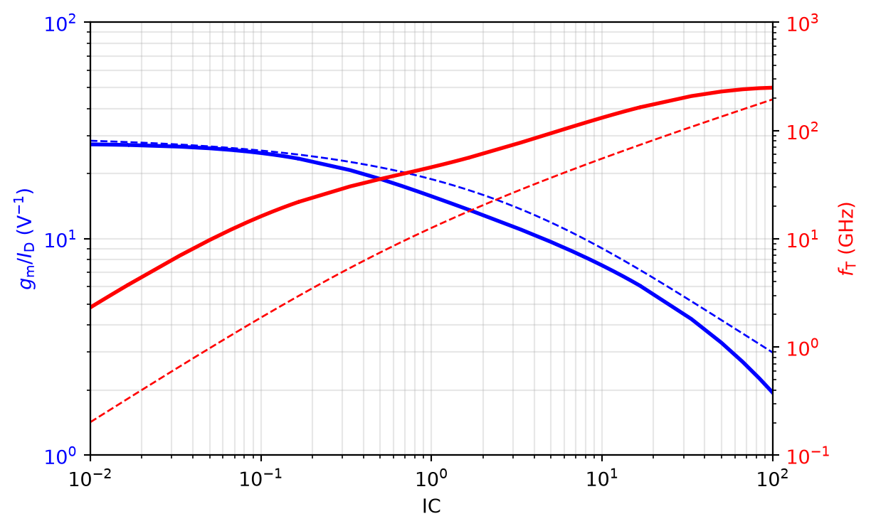
Figure 24 shows the same trade-off extracted from simulation data of an NMOS (\(W/L = 1.3\,\mu\text{m}/0.13\,\mu\text{m}\)) in IHP SG13. The simulation matches the analytical model well for \(g_\mathrm{m}/I_\mathrm{D}\); the simulated \(f_\mathrm{T}\) comes out higher than the simple model predicts, since the model pessimistically assumes the full \(\frac{2}{3} C'_\mathrm{ox}W L\) gate capacitance at all bias points, while at high \(\mathrm{IC}\) velocity saturation causes the simulated \(f_\mathrm{T}\) to flatten.
2.9.3 Sizing Procedure
The design procedure using the inversion coefficient is as follows:
- Depending on the trade-off between low power (high \(g_\mathrm{m}/I_\mathrm{D}\)) and high speed (high \(f_\mathrm{T}\)), select the \(\mathrm{IC}\) (often, \(\mathrm{IC}\approx 1\) is a reasonable compromise).
- Choose either the bias current or the required \(g_\mathrm{m}\), and calculate the other one using Equation 43.
- Using Equation 42, calculate \(I_\mathrm{S}\) from the known \(I_\mathrm{D}\).
- Depending on the requirements for transistor speed (minimum \(L\)), matching (large \(W \cdot L\)), or small \(g_\mathrm{ds}\) (large \(L\)), choose the appropriate \(L\); use Equation 40 to calculate the corresponding \(W\).
- Finally, estimate \(f_\mathrm{T}\) using Equation 44. From \(f_\mathrm{T}\), the required bandwidth of the circuit can be estimated, and the sizing can be iterated if necessary.
Now the most important transistor parameters (\(W\), \(L\), \(I_\mathrm{D}\), \(g_\mathrm{m}\), \(V_\mathrm{GS}\), and \(f_\mathrm{T}\)) are selected and known.
2.10 Summary
The MOSFET is a very versatile device, which can, depending on the bias conditions, work as a:
- Switch (for small \(V_\mathrm{DS}\) and large \(V_\mathrm{GS}\)).
- Voltage-controlled resistor (since \(g_\mathrm{ds}= f(V_\mathrm{GS})\) in the triode region).
- Voltage-controlled current source (since \(I_\mathrm{D}= f(V_\mathrm{GS})\) in the saturation region).
- Diode (since the MOSFET is off for \(V_\mathrm{GS}< V_\mathrm{th}\) and on otherwise).
- Variable capacitor (using the gate oxide or drain/source junction capacitance).
This versatility is nicely illustrated by the collection of two-transistor circuits in (Pretl and Eberlein 2021); the paper, plus posters showing all fifty circuits, is available at the Fifty Nifty Variations of Two-Transistor Circuits homepage.
When making the MOSFET physically small by scaling \(L \ll 1\,\mu\text{m}\) to improve power, performance, and area, various imperfections kick in (like DIBL), causing increased leakage currents and degraded output conductance—so alternative device constructions like SOI, FinFET, and nanosheet MOSFETs have been introduced.
2.11 Appendix: Silicon Material Properties
Table 5 collects the physical properties of silicon used throughout this text.
| Physical parameter of Si | Symbol | Typical value |
|---|---|---|
| Lattice constant | 0.54 nm | |
| Density | \(5.0 \times 10^{22}\,\text{cm}^{-3}\) | |
| Relative permittivity of Si | \(\varepsilon_\mathrm{r,si}\) | 11.9 |
| Relative permittivity of SiO2 | \(\varepsilon_\mathrm{r,ox}\) | 3.9 |
| Band gap at 300 K | \(E_\mathrm{bg}\) | 1.12 eV |
| Intrinsic carrier concentration at 300 K | \(n_\mathrm{i} = p_\mathrm{i}\) | \(1.0 \times 10^{10}\,\text{cm}^{-3}\) |
| Linear coefficient of thermal expansion | CTE | \(2.6 \times 10^{-6}\,\text{K}^{-1}\) |
| Melting point | 1415 °C | |
| Mobility of electrons at 300 K | \(\mu_\mathrm{n}\) | 1500 cm²/(V s) |
| Mobility of holes at 300 K | \(\mu_\mathrm{p}\) | 450 cm²/(V s) |
| Thermal conductivity | 1.5 W/(cm K) | |
| Breakdown field | \(E_\mathrm{crit}\) | \(3 \times 10^{5}\,\text{V/cm}\) |
3 IC Technology
This chapter walks through the manufacturing technology of integrated circuits: from the raw silicon wafer through the individual processing steps (doping, photolithography, etching, thin-film deposition, and interconnect formation) to a complete CMOS process flow. The treatment largely follows (Hu 2010).
3.1 The Silicon Wafer
The starting material for integrated-circuit production is, quite literally, sand: quartz sand (SiO2) is reduced with coal in an electric arc furnace at about 2000 °C to roughly 98 % purity, following the reaction \(\text{SiO}_2 + 2\,\text{C} \rightarrow \text{Si} + 2\,\text{CO}\). This “metallurgical-grade” silicon is then chemically purified via trichlorosilane (\(\text{Si} + 3\,\text{HCl} \rightleftharpoons \text{SiHCl}_3 + \text{H}_2\)), which can be distilled and decomposed back into ultra-pure silicon.
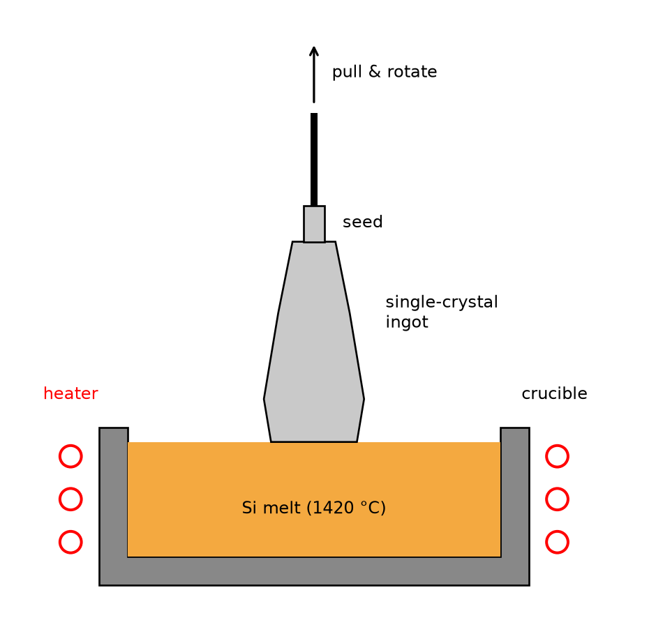
From the purified silicon, a large single crystal—the ingot—is grown by the Czochralski method, illustrated in Figure 25: a seed crystal is dipped into molten silicon and slowly pulled upwards while rotating, so that the melt crystallizes at the interface, continuing the crystal structure of the seed. Further purification can be achieved by zone refining, where a small molten zone is moved along the ingot, dragging impurities along; the final purity reaches 99.9999999 %, which is equivalent to one impurity atom per billion silicon atoms.
The ingot is then cut into wafers using a saw, to a thickness of 0.3 to 0.8 mm, and the wafers are polished. The standard wafer diameters today are 150 mm (6”), 200 mm (8”), and 300 mm (12”). The resistivity of the wafer material, set by doping, is 0.1 to 20 Ω cm, with up to 1000 Ω cm for specialty processes. Wafers can be \(n\)- or \(p\)-type, and often epitaxial (“epi”) wafers are used.
3.1.1 Doping
The silicon atoms are spaced roughly 0.24 nm apart in the crystal lattice, resulting in about \(5 \times 10^{22}\,\text{atoms/cm}^3\). The intrinsic carrier concentration is \(n_\mathrm{i} = p_\mathrm{i} \approx 1.0 \times 10^{10}\,\text{cm}^{-3}\) at 300 K, with an exponential temperature dependence (older textbooks often quote \(1.5 \times 10^{10}\,\text{cm}^{-3}\); the accepted measured value is \(9.65 \times 10^{9}\,\text{cm}^{-3}\) (Sproul and Green 1991)). By introducing doping materials in small quantities, the carrier concentration can be modulated strongly; see Table 6 (\(N_\mathrm{d}\) and \(N_\mathrm{a}\) are given in \(\text{cm}^{-3}\)).
| \(n\)-type (donor materials) | \(p\)-type (acceptor materials) | |
|---|---|---|
| Effect | Introduces additional free electrons | Introduces a lack of electrons (“holes”) |
| Elements | Phosphorus (P), Arsenic (As) | Boron (B), Gallium (Ga), Indium (In) |
| Carrier concentrations | \(n_0 \approx N_\mathrm{d}\), \(p_0 \approx n_\mathrm{i}^2 / N_\mathrm{d}\) | \(p_0 \approx N_\mathrm{a}\), \(n_0 \approx n_\mathrm{i}^2 / N_\mathrm{a}\) |
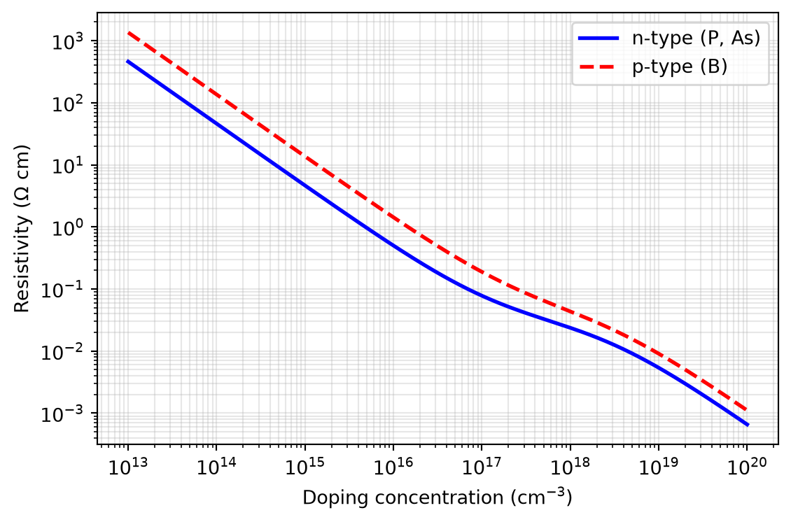
The resulting resistivity of doped silicon is shown in Figure 26 as a function of the doping concentration.
Note 3: Example: Wafer Doping
Let us assume a \(p\)-type wafer with 50 Ω cm resistivity (as used in IHP SG13 CMOS). Using Figure 26, we find \(N_\mathrm{a}= p_0 \approx 2.7 \times 10^{14}\,\text{cm}^{-3}\), which results in \(n_0 \approx n_\mathrm{i}^2 / N_\mathrm{a}= 3.7 \times 10^{5}\,\text{cm}^{-3}\). This doping concentration equates to about one acceptor atom per 180 million silicon atoms!
3.2 Selective Doping
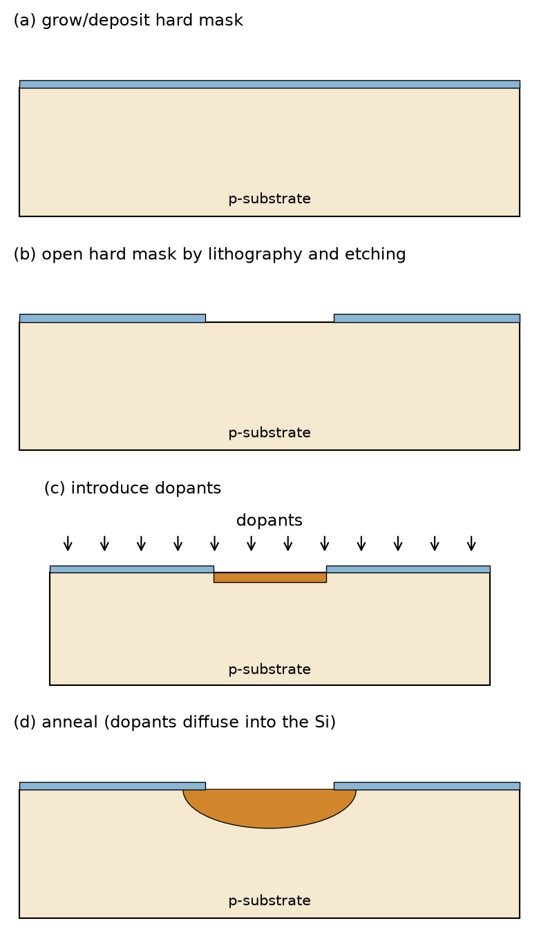
To introduce dopants into the silicon wafer selectively, a masking process is used:
- The picture from a photomask is optically transferred into a photoresist on the wafer, using a process called photolithography.
- This photoresist is developed and used to selectively etch a masking layer, like SiO2 (a “hard mask”).
- After this step, the silicon surface is opened at specific locations and covered otherwise, allowing the introduction of dopants into defined areas of the wafer.
The complete sequence—hard-mask formation, lithography, etching, dopant introduction, and annealing (which removes defects from the crystal structure while the dopants diffuse into the silicon)—is shown in Figure 27.
3.2.1 Oxidation of Silicon
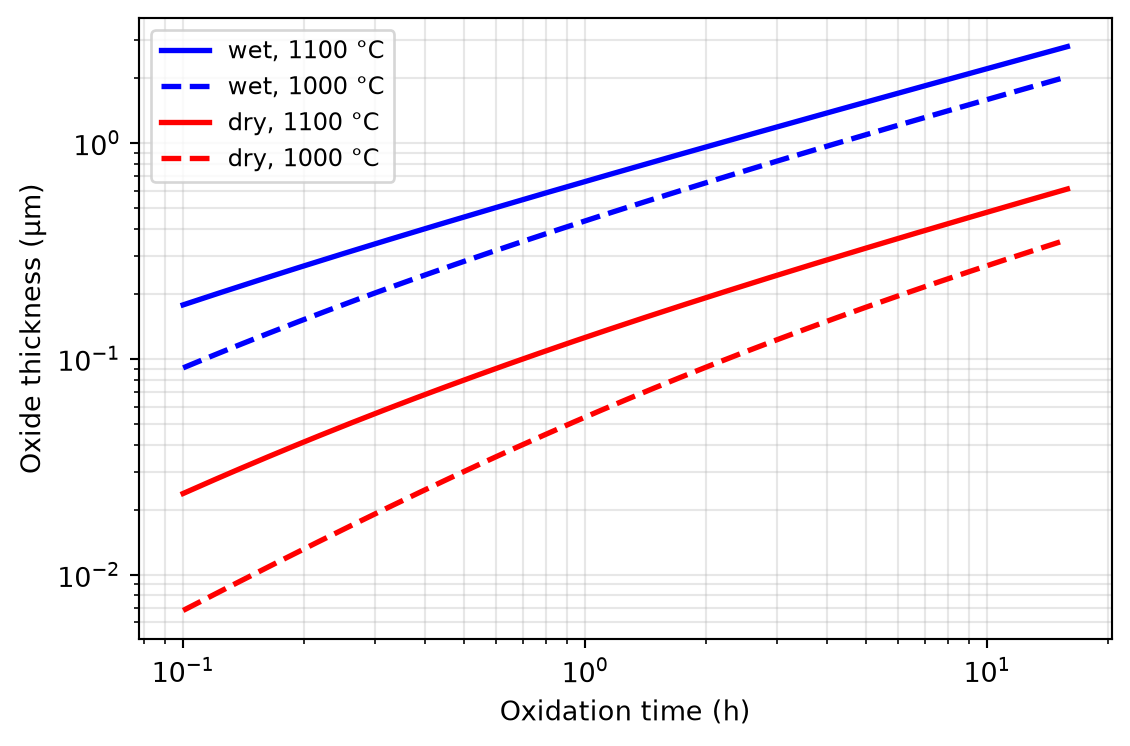
Oxidation of silicon is done at elevated temperatures in a furnace, using either “dry” (\(\text{Si} + \text{O}_2 \rightarrow \text{SiO}_2\)) or “wet” (\(\text{Si} + 2\,\text{H}_2\text{O} \rightarrow \text{SiO}_2 + 2\,\text{H}_2\)) oxidation. The oxide growth follows the Deal-Grove model (Deal and Grove 1965); the resulting growth curves are shown in Figure 28. Wet oxidation is much faster, while dry oxidation yields denser, higher-quality oxides (used, e.g., for gate oxides).
The SiO2 is used for:
- The gate dielectric of the MOSFET.
- Hard masks for implantation or doping.
- Device isolation and isolation of wiring.
The growth of SiO2 consumes silicon; the silicon thickness is reduced by 44 % of the grown oxide thickness. Alternatively, chemical vapour deposition (CVD) can be used for depositing SiO2 without consuming silicon. Local oxidation of silicon (LOCOS) can be used to laterally isolate active regions of an integrated circuit, but in modern CMOS technologies shallow trench isolation (STI) is used instead, for higher transistor density.
3.3 Photolithography
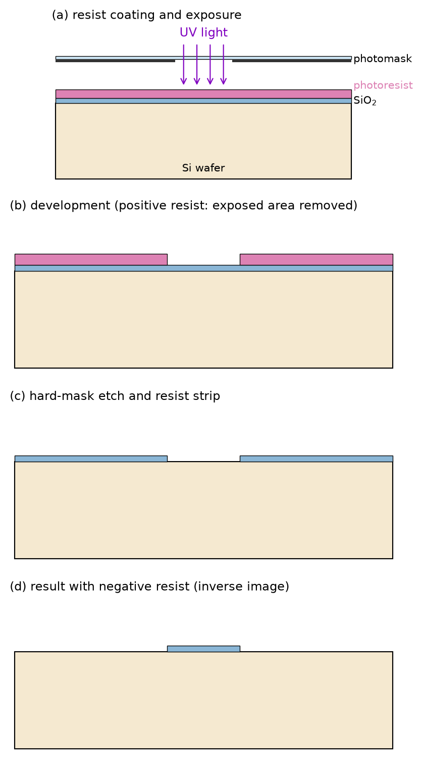
In photolithography, the wafer is first oxidized to create a hard-mask layer and then coated with photoresist. The photomask is imaged onto the photoresist with a projection lens system, the resist is developed and baked, and the hard mask is etched through the resist openings. There are two types of resist: with a positive resist, the exposed areas dissolve in the developer, transferring the mask image directly; with a negative resist, the exposed areas remain, creating an inverse image. After etching, the remaining photoresist is removed. The process is illustrated in Figure 29.
3.3.1 Photomasks
Instead of a photomask which exposes the whole wafer at once, a reticle is mostly used, which is smaller than the wafer, with a field size of ca. 26 mm × 33 mm (limiting the maximum die size to 858 mm²). A stepper exposes the complete wafer field by field with the reticle. The photomask/reticle is usually made of a glass carrier with a structured chromium layer.
The reticle must be protected from contamination, so a thin transparent membrane (called a pellicle) keeps particles out of the focal plane, away from the mask structures. The reticle can be the same size (1×) or larger (2× or 4×) than the structures on the wafer, and the photomask can touch the wafer (“contact printing”) or be kept at a distance (“proximity printing”)—modern lithography uses projection printing through a reduction lens.
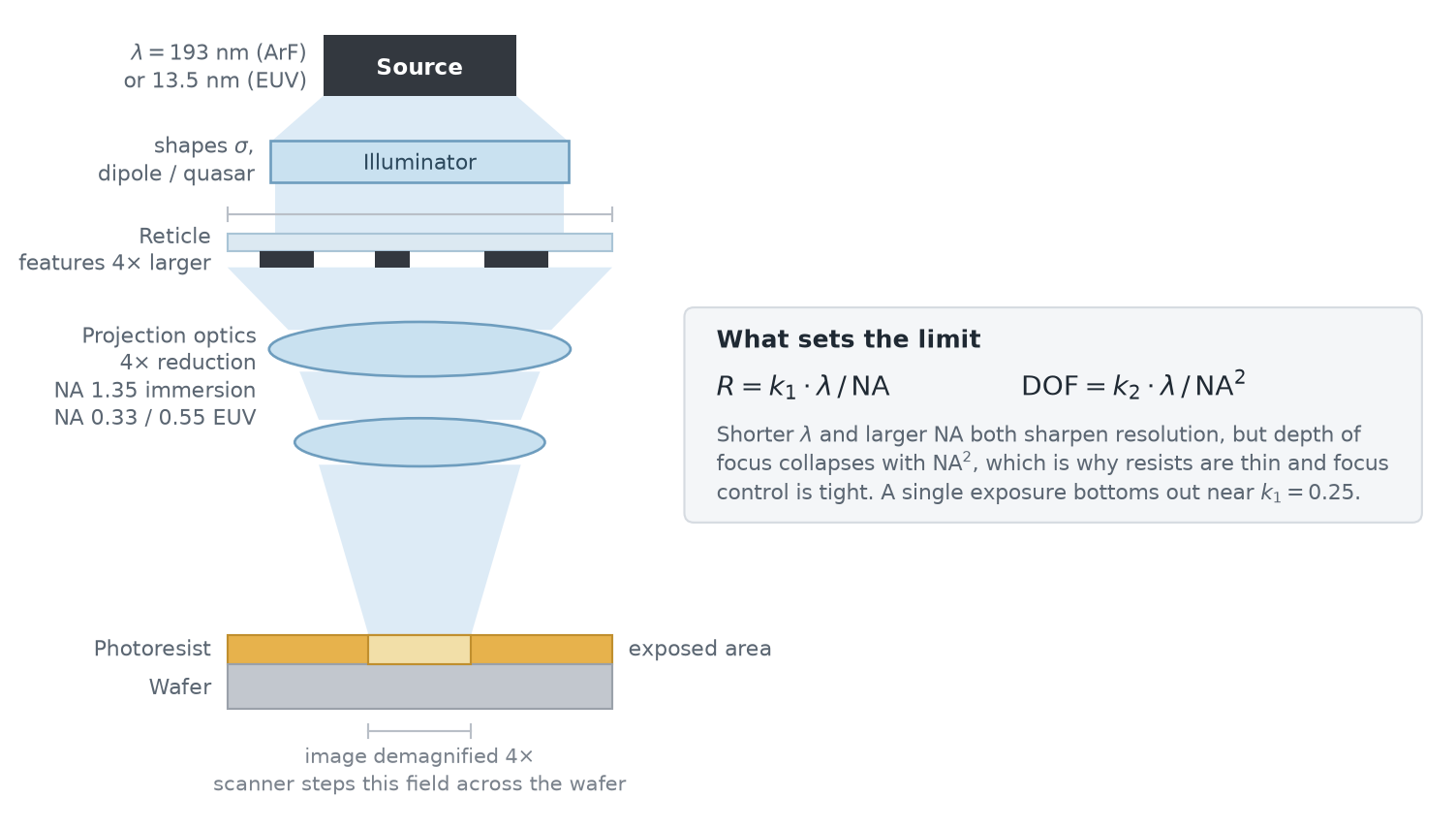
The complete exposure system is shown in Figure 30. The light passes from the source through the illuminator, which shapes the angular distribution of the illumination (e.g. into a dipole or quasar pattern), onto the reticle; the projection optics then image a demagnified copy of the reticle field into the resist, and the scanner steps this field across the wafer, one exposure at a time.
3.3.2 Resolution Limit
As in any other optical system, the resolution limit of photolithography is given by the Rayleigh criterion:
\[ R = k_1 \frac{\lambda}{n \sin \Theta} = k_1 \frac{\lambda}{\mathrm{NA}} \tag{45}\]
Here, \(\lambda\) is the wavelength of the light source, and \(k_1\) is a factor that captures various resolution-enhancement measures, like phase-shift masks or off-axis illumination (\(0.25 \leq k_1 \leq 1\)). \(\mathrm{NA}\) is the numerical aperture of the lens system (in air, \(\mathrm{NA} \leq 0.93\)). The resulting half-pitch \(R\) is the smallest pattern that can be printed on a wafer: \(R = 100\,\text{nm}\) means that lines with a width of 100 nm and a spacing of 100 nm can be printed.
Resolution is not free. The depth of focus, i.e. the range over which the projected image stays sharp, shrinks with the square of the numerical aperture:
\[ \mathrm{DOF} = k_2 \frac{n \lambda}{\mathrm{NA}^2} \tag{46}\]
Here, \(k_2\) is the depth-of-focus counterpart of \(k_1\): it captures how much image degradation the process still tolerates, set by resist contrast and thickness, feature type and illumination scheme (\(0.5 \leq k_2 \leq 1\)). The two factors pull against each other—the same off-axis illumination that buys a small \(k_1\) also shrinks \(k_2\), so pushing resolution costs focus budget twice. Note that the refractive index \(n\) does not cancel here: raising \(n\) recovers depth of focus at a given \(\mathrm{NA}\).
This is why resists are kept thin and why the wafer surface must be held in focus to within a few tens of nanometers while the field is scanned.
3.3.3 Light Sources
In the 1980s, mercury lamps with \(\lambda = 436\,\text{nm}\) (g-line) or \(\lambda = 365\,\text{nm}\) (i-line) were used. Starting with 0.25 µm CMOS (until 180 nm), excimer lasers with \(\lambda = 248\,\text{nm}\) were introduced, called deep-ultraviolet (DUV) light. Since 130 nm CMOS, ArF lasers with \(\lambda = 193\,\text{nm}\) are used, which can be combined with multi-patterning to break the half-pitch limit of \(R \approx 40\,\text{nm}\). Finally, extreme-ultraviolet (EUV) lithography was introduced at the 7 nm CMOS node, offering a huge reduction in wavelength to \(\lambda = 13.5\,\text{nm}\)—accompanied by an extreme cost impact due to the need for all-reflective optics.
Note that there is only one company in the world that currently manufactures EUV lithography machines: ASML from the Netherlands. This gives ASML a unique position in the semiconductor equipment market, as EUV is critical for advanced nodes. Zeiss from Germany produces the high-precision optics required for these machines. Further, there is only one company in the world that makes the multi-beam mask writers needed for creating the EUV masks: IMS Nanofabrication from Austria.
3.3.4 Resolution Enhancements
Various methods are used to reduce the half-pitch in Equation 45 by compensating distortion due to diffraction and interference, modifying either the amplitude or the phase of the light:
- Optical proximity correction (OPC) enhances the contrast of critical layout features like line ends and corners by pre-distorting the mask shapes.
- Phase-shift masks (PSM) vary the thickness of the mask, so that phase changes of the light can be used for contrast enhancement.
- Immersion lithography uses the refractive index of water (\(n = 1.44\)) between lens and wafer to achieve \(\mathrm{NA} > 1\); per Equation 46, the higher \(n\) also restores part of the depth of focus lost to the larger \(\mathrm{NA}\).
Ultimately, using these techniques, structures considerably smaller than the wavelength of the used light can be printed.
3.3.5 EUV Lithography
EUV light at 13.5 nm is created by firing laser pulses at molten tin droplets. There are no transmissive lens materials for EUV, so the optics are constructed from reflective mirrors with about 30 % loss per mirror. A first-generation EUV scanner is a 180-tonne machine using 0.5 MW of electrical power to create roughly 200 W of optical power at the wafer, processing about 200 wafers per hour. Comparing the achievable resolution:
- ArF immersion lithography: \(\lambda = 193\,\text{nm}\), \(\mathrm{NA} = 1.35\), \(k_1 = 0.27\) (with PSM) \(\Rightarrow\) \(R \approx 40\,\text{nm}\).
- First-generation EUV (NXE): \(\lambda = 13.5\,\text{nm}\), \(\mathrm{NA} = 0.33\), \(k_1 = 0.32\) \(\Rightarrow\) \(R \approx 13\,\text{nm}\).
- Current high-NA EUV (EXE): \(\lambda = 13.5\,\text{nm}\), \(\mathrm{NA} = 0.55\), \(k_1 = 0.32\) \(\Rightarrow\) \(R \approx 8\,\text{nm}\).
3.4 Etching
Etching is used to transfer the image from the photoresist into the hard mask (or from one layer into another layer) by selectively removing material. Etching can be isotropic or anisotropic, characterized by the anisotropy \(A\); the selectivity \(S\) measures the ratio of the etch rate of the film to the etch rate of the mask. An optimal etch has \(A=1\) (only vertical etching, no lateral etch) and \(S=\infty\) (the mask is not attacked). Two types of etches are used:
- Wet etching, using liquid chemicals (typically isotropic).
- Dry etching, using chemically active ionized gases in a plasma reactor (can be highly anisotropic).
3.5 Doping Techniques
Three methods of introducing dopants into the silicon can be used:
- Diffusion: dopants move (by diffusion) from the wafer surface into the wafer material; the source of the dopants is a gas (e.g., POCl3 for phosphorus doping) or a solid film on the wafer surface.
- Ion implantation: dopants are ionized, accelerated, and shot into the wafer material.
- Epitaxy: additional silicon is grown on the wafer surface and doped in situ while growing the silicon layer.
3.5.1 Diffusion
Diffusion is the movement of impurity atoms from the surface into the bulk of the silicon, performed at high temperatures (900 to 1200 °C). There are two limiting cases:
- Infinite source of impurities at the surface: the resulting doping profile follows a complementary error function (erfc).
- Finite source of impurities at the surface: the resulting doping profile is a Gaussian, \(N(x,t) = N_{0}/\sqrt{\pi D t} \cdot \exp(-x^{2} / (4 D t))\), with \(x\) the distance from the wafer surface, \(N_0\) the initial dopant dose per area, \(D\) the diffusivity, and \(t\) the diffusion time.
The drawback of diffusion is that the doping concentration is always highest at the wafer surface and constrained to these profile shapes.
3.5.2 Ion Implantation
Ion implantation lodges impurity ions into the target material at high velocity; implantation can even be done through surface layers (e.g., through the gate oxide for threshold-voltage adjustment). The resulting doping depth profile is
\[ N(x) = \frac{N_\mathrm{i}}{\sqrt{2 \pi} \, {\Delta R}} \, e^{-\frac{(x-R)^2}{2 {\Delta R}^2}} \tag{47}\]
which peaks at the projected range \(R\); the straggle \(\Delta R\) is tied to \(R\), so the achievable profiles are also constrained (\(N_\mathrm{i}\) is the implanted dose per area). A subsequent anneal (typically a rapid thermal anneal at 900 to 1100 °C) is required to activate the impurities and to repair the damage to the crystal lattice. Figure 31 compares typical diffusion and implantation profiles.
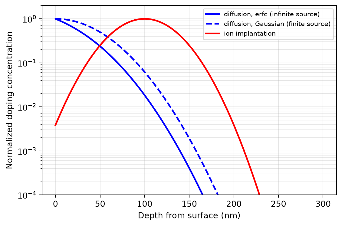
3.5.3 Epitaxy
Epitaxial growth forms a layer of single-crystal silicon on the surface of the wafer, such that the crystal structure is continuous across the interface. The epi layer can be doped differently from the material where it is grown, with a typical thickness of 1 to 20 µm (patterned epitaxial growth using a mask is also possible).
3.6 Thin-Film Deposition
Various thin films are used in IC processing:
- The gate dielectric of the MOSFET, like SiO2 (either thermally grown or deposited via CVD).
- The gate material, polysilicon, which is also used for local interconnects and resistors.
- Metal films for interconnects (metals like Al or Cu, and silicides like TiSi2, WSi2, TaSi2, NiSi2).
- Contact and via materials, like W, Al, or Cu.
- Dielectrics between metal layers and spacers, like SiO2 and Si3N4.
These films are either sputtered or deposited from chemical gases in chemical vapour deposition (CVD); both methods are sketched in Figure 32. Exemplary chemical reactions for CVD are:
- Depositing polysilicon: \(\text{SiH}_4 \rightarrow \text{Si} + 2\,\text{H}_2\)
- Depositing SiO2 (as an alternative to thermal oxidation): \(\text{SiH}_4 + \text{O}_2 \rightarrow \text{SiO}_2 + 2\,\text{H}_2\) or \(\text{SiH}_2\text{Cl}_2 + 2\,\text{N}_2\text{O} \rightarrow \text{SiO}_2 + 2\,\text{HCl} + 2\,\text{N}_2\)
- Depositing Si3N4: \(3\,\text{SiH}_2\text{Cl}_2 + 4\,\text{NH}_3 \rightarrow \text{Si}_3\text{N}_4 + 6\,\text{HCl} + 6\,\text{H}_2\)
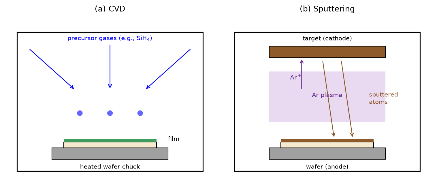
3.7 Interconnects
In the so-called back-end of the process, the devices formed in the front-end (like MOSFETs and resistors) are connected by a sandwich of metallic and dielectric thin films. The metal layers are connected through the dielectric layers by vias (between metals) and contacts (from the lowest metal layer to the front-end devices).
Historically, aluminum has been used as the interconnect metal, as it can be deposited by sputtering and then patterned by etching. However, Al is prone to void formation by electromigration. In newer technologies, copper is used: its resistance is 40 % lower, and it has excellent electromigration reliability. However, dry etching of Cu is difficult, so a damascene process is used, shown in Figure 33: the dielectric is structured, a liner and Cu are deposited into the trenches, and the excess metal is removed by chemical-mechanical polishing (CMP). The liner prevents the Cu from diffusing into the dielectric.
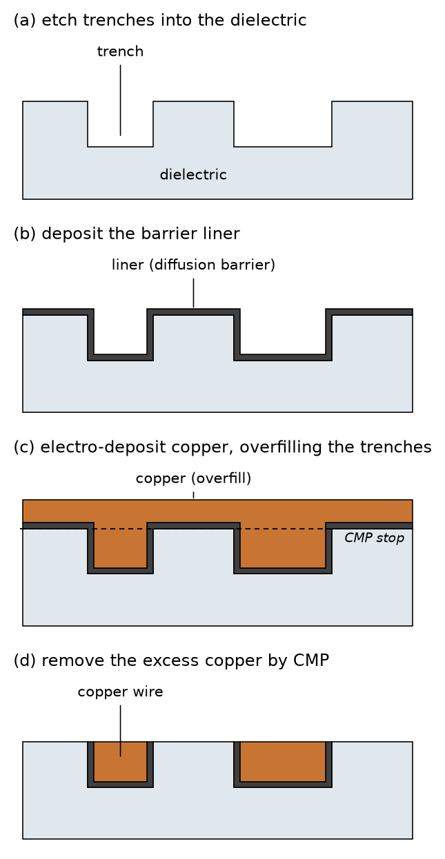
The classic dielectric between the metal layers is SiO2, but in order to reduce capacitive parasitics, low-k dielectrics (e.g., F- or C-doped SiO2) are used in modern processes. Between processing steps, CMP is used to planarize the surfaces.
3.8 An Exemplary CMOS Process Flow
The following figures illustrate a simplified CMOS process flow, inspired by the openly documented LibreSilicon process; the cross sections show an NMOS (in the p-well) and a PMOS (in the n-well), each with its well tap on the outside, evolving through the process steps.
Step 1—Shallow trench isolation: After an initial cleaning, a hard mask (SiO2 or Si3N4) is grown/deposited and patterned by photolithography. The isolation trenches are etched anisotropically and filled with oxide (Figure 34).
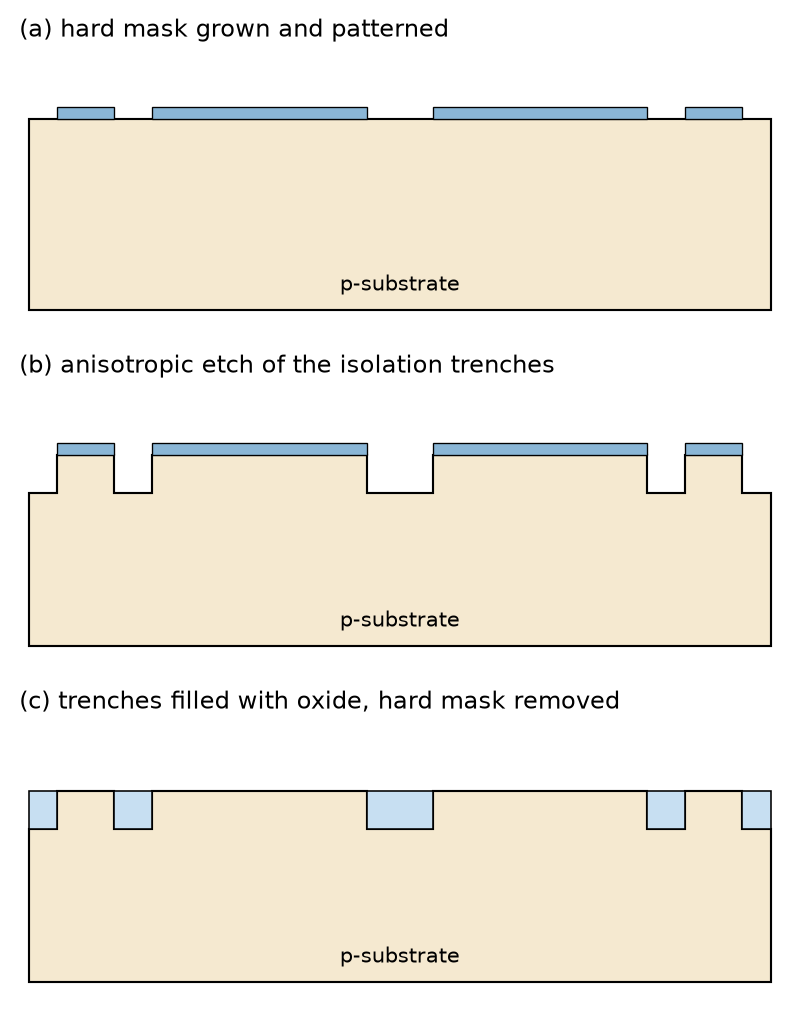
Steps 2 and 3—Well formation: A hard mask is formed and opened over the p-well region, boron is implanted, and the wafer is annealed. The sequence is repeated with phosphorus for the n-well (Figure 35).
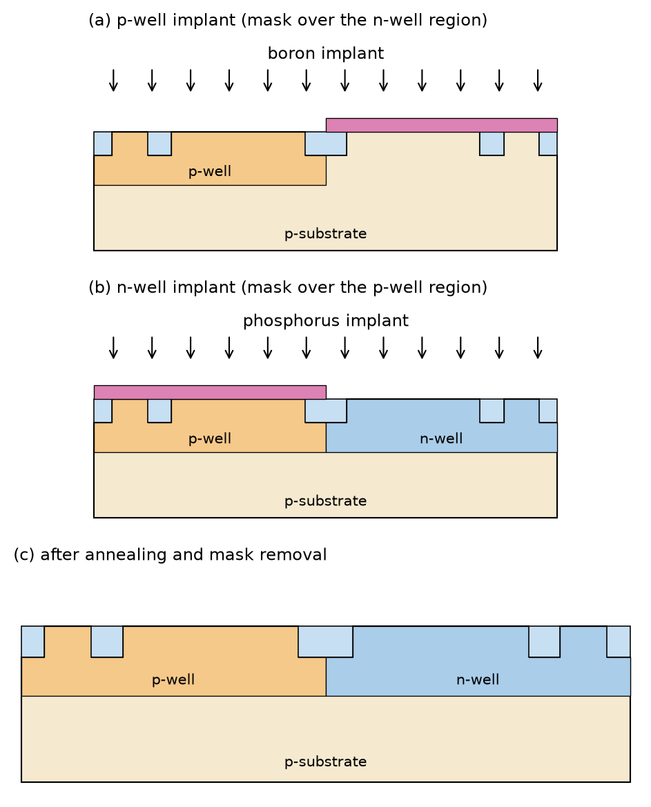
Steps 4 and 5—Gate formation: A field oxide is grown and removed over the active areas; then the thin gate oxide is grown by dry oxidation, polysilicon is deposited by CVD, and the gate stack is patterned (Figure 36).
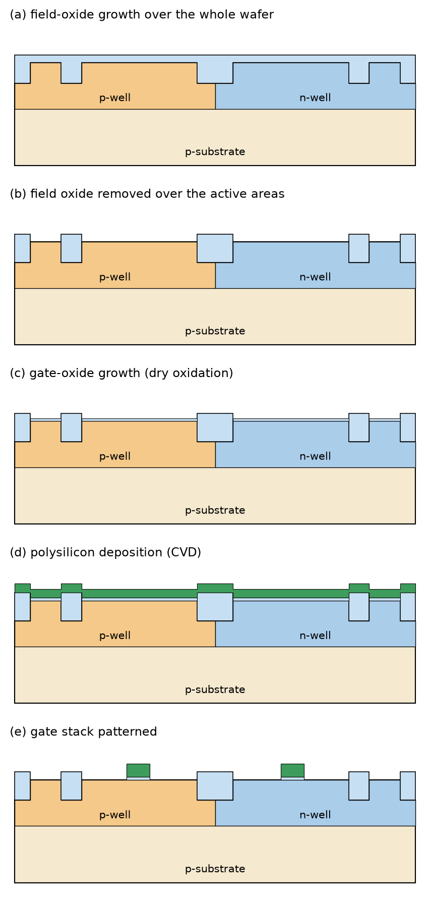
Steps 6 and 7—Source/drain implants: With photoresist masking the PMOS area, phosphorus is implanted to form the NMOS source/drain regions (and the n-well contacts); the implant is self-aligned to the gate, which acts as an implantation mask for the channel region. The complementary boron implant forms the PMOS source/drain regions (and the p-well contacts). Each implant is followed by an anneal (Figure 37).
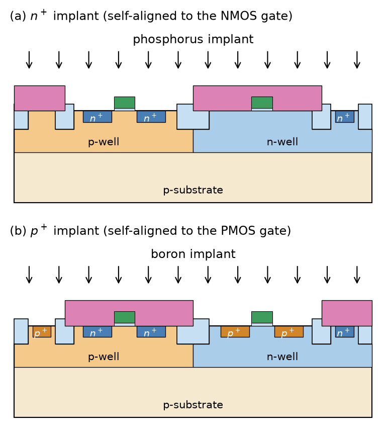
Step 8—Silicide formation: An oxide/nitride layer is deposited and anisotropically etched, leaving spacers at the gate edges. Titanium is sputtered onto the wafer and reacts where it touches silicon, forming low-resistance TiSi2 on the source/drain areas and the gate; the unreacted metal is removed (Figure 38).
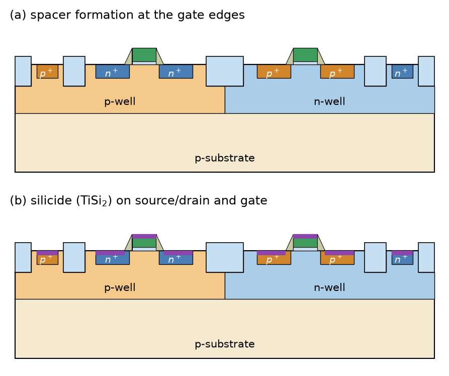
Steps 9 to 11—Contacts and metal stack: An inter-layer dielectric is deposited and planarized by CMP, contact holes are etched and filled, and the first metal layer is deposited and patterned. Further levels of dielectric, vias, and metal follow; finally, the passivation is deposited and opened at the pads (Figure 39).
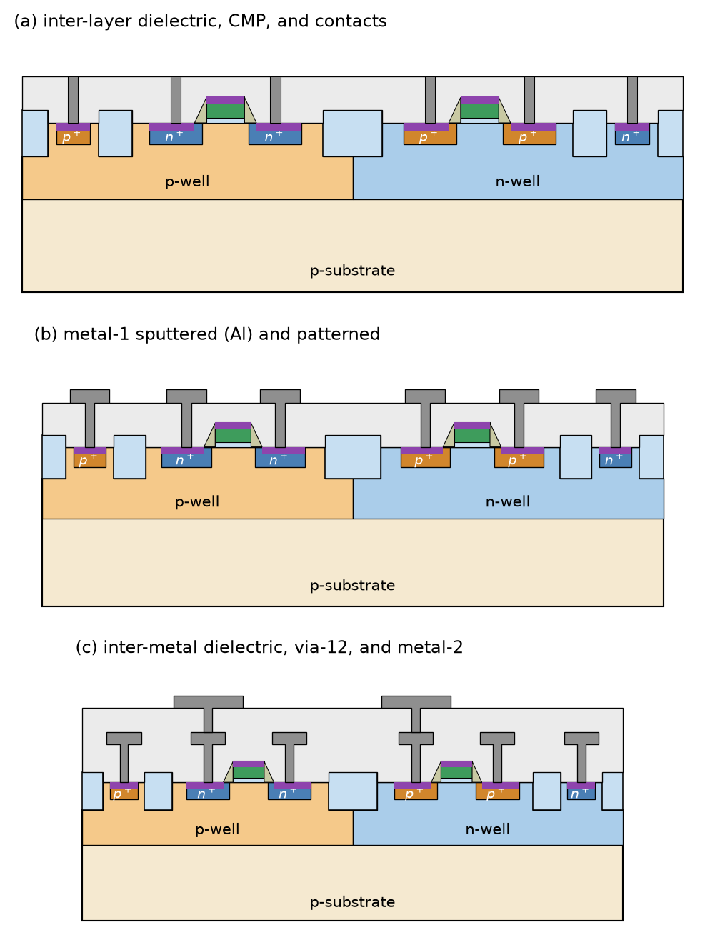
3.9 The Open-Source PDK IHP SG13
IHP has open-sourced the process design kit (PDK) for a 130 nm BiCMOS technology (the current generation is named SG13G2, referred to here simply as IHP SG13) under the Apache-2.0 license. The relevant files, including documentation, can be found at github.com/IHP-GmbH/IHP-Open-PDK. This technology has a lot of interesting features:
- Support for internal 1.2 V/1.5 V core MOSFETs and 3.3 V I/O MOSFETs
- An aluminum metal stack with 5 thin and 2 thick levels of metal (see Figure 40)
- Silicided, standard, and high-sheet-rho poly resistors
- A metal-insulator-metal (MIM) capacitor
- A Schottky diode
- Optional high-speed SiGe:C heterojunction bipolar transistors (HBTs)
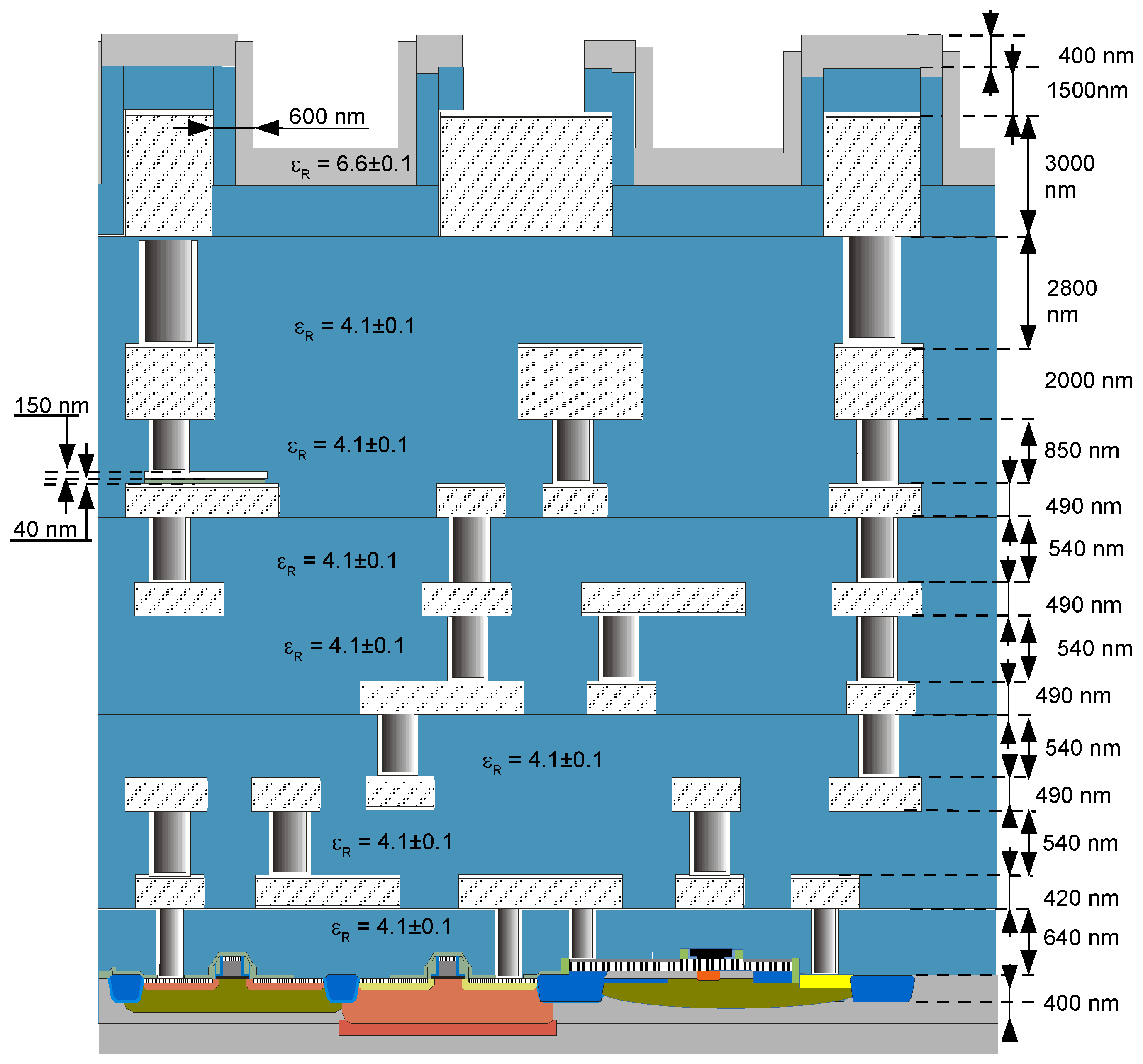
3.10 Technology Qualification
Before a product in a certain semiconductor technology is shipped to customers, a qualification procedure has to be completed. Its purpose is to demonstrate, on a statistically meaningful sample and before the first customer shipment, that the product will meet its datasheet over the intended lifetime and operating conditions. The overall framework is set by JEDEC JESD47 (Stress-Test-Driven Qualification of Integrated Circuits), which references the individual test methods; automotive products additionally follow AEC-Q100, which defines temperature grades and larger sample sizes. Table 7 lists typical tests.
| Test (examples) | Standard | Motivation & check |
|---|---|---|
| HTOL (high-temperature operating life) | JESD22-A108 | Subject the IC to high temperature under operation over an extended duration. |
| ESD HBM | JS-001-2023 | ESD test, human-body model. |
| ESD CDM | JS-002-2022 | ESD test, charged-device model. |
| Latch-up | JESD78 | Latch-up test. |
| Electrical test (ED) | JESD86 | Check conformance to the datasheet across conditions and lots. |
These tests fall into three groups: lifetime tests that accelerate wear-out, robustness tests that check survival of a single electrical stress event, and electrical verification against the datasheet.
HTOL stresses a sample of packaged devices—typically three lots of 77 parts, so that zero failures give a meaningful confidence bound—at an elevated junction temperature, usually 125 °C and often combined with a supply voltage above nominal, while the circuit is electrically exercised, for a duration of typically 1000 h. It accelerates exactly those wear-out mechanisms that limit the life of a MOSFET: time-dependent dielectric breakdown (TDDB) of the gate oxide, hot-carrier injection (HCI), bias temperature instability (BTI), and electromigration in the interconnect. Since these mechanisms are thermally activated, an Arrhenius acceleration factor—commonly in the range of 20 to 100—translates the 1000 h of stress into years of operation at the application temperature. A device fails the test if it stops working, or if any parameter has drifted outside the datasheet limits.
ESD HBM models the electrostatic discharge of a charged person touching a pin. The human-body model discharges a 100 pF capacitor through a 1.5 kΩ resistor, which produces a comparatively slow pulse (rise time of a few nanoseconds, decay time constant of 150 ns) with a peak current of about 0.67 A per kV. Every pin is stressed against every supply, in both polarities; a common target is 2 kV. The protection consists of diodes at each pad plus a clamp across the supply, arranged so that there is a low-impedance path between any two pins—which is why ESD protection is a full-chip problem, not a per-pad one.
ESD CDM models the opposite situation: the device itself has been charged, for example by sliding through a shipping tube, and discharges when one of its pins touches a grounded surface. The charged-device model pulse is far faster than HBM, with a rise time below 500 ps and a total duration of about 1 ns, reaching peak currents of several amperes. Because the pulse is largely over before the protection structures have fully turned on, CDM is usually the harder of the two to pass, and it is the more relevant one in modern automated assembly, where a human rarely touches the parts. The stored charge grows with package size, so large packages are stressed hardest. A typical target is 500 V, and interfaces between separate supply domains are the classic weak spot.
Latch-up targets the parasitic thyristor that is inherent to every CMOS well structure: the source of a PMOS, the n-well, the p-substrate, and the source of a neighboring NMOS form a PNPN structure, equivalent to a pair of cross-coupled parasitic bipolar transistors. If enough current is injected into a well—by an I/O pin driven beyond a supply rail, or by a supply overshoot—the structure latches into a low-impedance state that shorts supply to ground and persists until the power is removed, usually destroying the chip. JESD78 therefore injects ±100 mA into the I/O pins and applies an overvoltage to the supplies, at the maximum operating temperature. The countermeasures are all layout measures: a generous number of well and substrate taps, which is why the flow above places one next to each transistor (Figure 37), guard rings around injecting circuits, and minimum-spacing rules between NMOS and PMOS.
Electrical test (ED) is not a stress test. It assesses the electrical parameters of devices from the manufacturing and test process being qualified, verifying that they meet every datasheet parameter across the specified supply-voltage and temperature range, and that they do so consistently across several production lots. This is what catches a systematic process shift that leaves the technology inside its own control limits, but the product outside its specification.
A complete qualification also covers the package rather than the silicon, with temperature cycling, highly accelerated stress testing (HAST) for moisture resistance, and solder-reflow sensitivity (see Section 5.6).
4 The Layout
The layout is the 2D representation of the IC manufacturing data. While the schematic captures the electrical intent of a design, the layout captures its physical realization: in the layout tools, the design is drawn on several layers, which are the foundation for the generation of the photomasks used in IC production. Commercial layout tools are, e.g., Cadence Virtuoso, Siemens L-Edit, and open-source tools are Magic and KLayout. The layers are usually manipulated before the geometries are transferred to the masks (shrink, enlarge, invert, combination of several layers into one mask layer, optical proximity correction, etc.).
4.1 Files and Tapeout
The layout is checked for compliance with the wafer-fab design rules in the design rule check (DRC), and for conformance with the intended circuit in the layout-versus-schematic (LVS) check, where a netlist extracted from the layout is compared to the netlist of the original schematic. If all checks pass, the layout data is sent to mask production—this step is called tapeout. The mask house processes the layout data and produces the photomasks used by the wafer fab (depending on technology complexity, between 10 and 80 masks).
The standard file format for layout data is GDSII, a hierarchical database in a binary stream format. A newer format with more efficient storage is OASIS, but GDSII is still very common.
4.2 Generic Layer Definition
Different foundries use different layer names. The layer names defined in Table 8 are quite typical for a basic CMOS process technology and are used for the remainder of the text; the corresponding IHP SG13 names are given for reference.
| Layer name | IHP SG13 | Purpose |
|---|---|---|
RX |
Activ |
\(n^+\) (RX) or \(p^+\) (RX in BP) diffusion regions (e.g., S/D of MOSFETs) |
PC |
GatPoly |
Polysilicon gate |
NW |
NWell |
\(n\)-well region |
BP |
pSD |
\(p\)-implant marker (i.e., blocks the \(n\)-implant) |
OP |
SalBlock |
Silicide blocking over PC and RX |
CA |
Cont |
Contact (connects RX or PC to M1) |
M1 |
Metal1 |
First-level metal |
V1 |
Via1 |
Via connecting M1 to M2 |
M2 |
Metal2 |
Second-level metal |
V2 |
Via2 |
Via connecting M2 to M3 |
M3 |
Metal3 |
Top metal, mostly aluminum, to facilitate wire-bond packages |
PAD |
Passiv |
Opening in the passivation to contact the top metal for pads |
4.3 Devices
4.3.1 NMOS and PMOS Transistors
Figure 41 shows the layout (mask top view) of an NMOS and a PMOS transistor. The following observations can be made:
- The MOSFET is created by the intersection of
RXandPC; this intersection defines \(W\) and \(L\) of the transistor. The areas ofRXnot covered byPCbecome the source and drain regions. - Whether a device is NMOS or PMOS is decided by whether the
RXshape is contained inside aBPregion (RXplusBPis \(p^+\),RXwithoutBPis \(n^+\)). - A \(p^+\) substrate contact is created by drawing
RXcovered byBP(outside the n-well). - An \(n^+\) well contact is created by drawing plain
RXlocated insideNW. - The
NWmust surround the PMOS with sufficient margin. - The layer
BPis a pure marking layer, assisting mask generation and device extraction from the layout. CAcontacts connect source/drain/gate as well as the \(p^+\)/\(n^+\) contacts toM1.
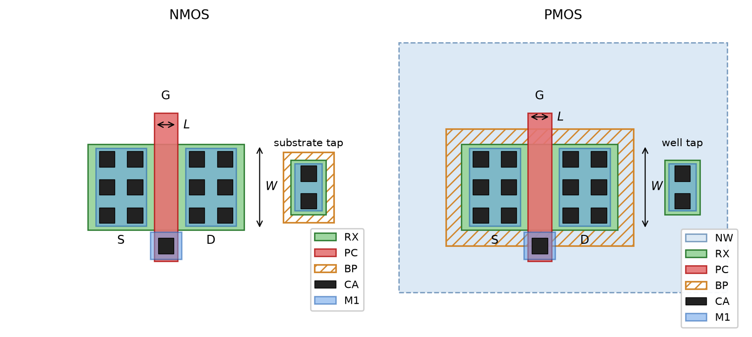
PC crosses RX; the BP marker turns the diffusion \(p^+\), and the NW well surrounds the PMOS. The area where PC overlaps RX is the actual transistor channel, defining its \(W\) and \(L\). Next to each transistor sits the corresponding substrate or well contact. Note that BP acts as a marking layer, whereas RX, PC, and NW define the actual device regions on the silicon.
4.3.2 Polysilicon Resistor
The polysilicon resistor (Figure 42) uses the gate material (PC) as a resistive device. Since the gate poly is normally covered by silicide to lower its resistance, the silicide is suppressed with an OP shape; the intersection of OP with PC precisely defines the \(L\) and \(W\) of the resistor. Note that the existence of OP is a process option and might not be available in every technology. The gate polysilicon can be either \(p\)- or \(n\)-type; \(p\)-type poly resistors are often preferred, as they offer a lower temperature coefficient (thus the PC is marked with BP).
The resistance value of the polysilicon resistor is given by (\(R_\square\) is the sheet resistance in Ω/\(\square\))
\[ R = \rho \frac{L}{t \cdot W} = R_\square \frac{L}{W} \tag{48}\]
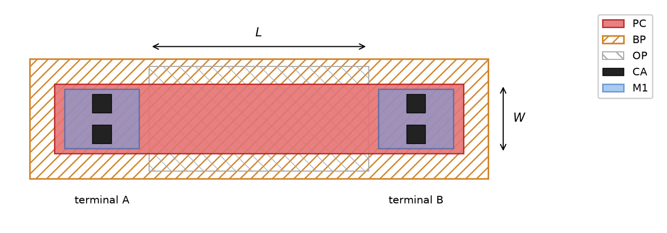
PC strip is blocked by the OP shape, whose intersection with PC defines the resistor body of length \(L\) and width \(W\); the BP marker selects \(p\)-type poly. The silicided ends are contacted with CA and M1.
Note that modern FinFET technologies might not support traditional planar polysilicon resistors, as the gate material is used to form the fins rather than a continuous sheet. In this case, often a metal resistor implemented in the back-end layers is used as an alternative.
4.3.3 Diffusion Resistor
Diffusion resistors (Figure 43) use source/drain diffusions or wells (with or without silicide) and are available in basically all silicon technologies, but they are usually inferior to polysilicon resistors: they have larger tolerances and a relatively high voltage coefficient, which can cause nonlinearity, and the nonlinear parasitic junction capacitance to the substrate can be critical as well. In older technology nodes (> 0.25 µm), the matching of diffusion resistors was better than that of poly resistors. One clear advantage of diffusion resistors is reduced self-heating, as the resistor body is embedded in the silicon substrate, whereas poly resistors are isolated from the substrate by SiO2. So resistor with increased power dissipation can benefit from this property.
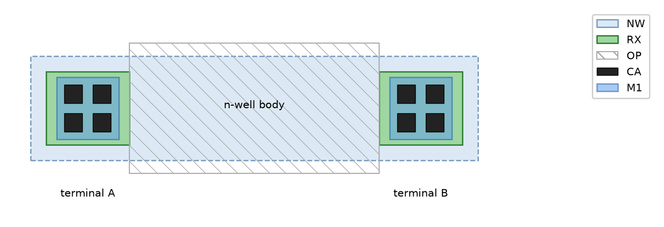
NW strip, contacted at both ends by \(n^+\) diffusions (RX); the OP shape blocks the silicide over the body. The parasitic junction to the substrate makes this resistor nonlinear with the applied voltage.
The resistor types available in IHP SG13 are summarized in Table 9.
| Type | \(R_\square\) (Ω/\(\square\)) | Process tolerance (\(\pm 4 \sigma\)) | Matching | Temp. coefficient |
|---|---|---|---|---|
Silicided \(n^{++}\)-poly (rsil) |
7 | ±12 % | 0.6 %µm | 0.3 %/K |
Blocked \(p^+\)-poly (rppd) |
260 | ±10 % | 1.5 %µm | 0.017 %/K |
Blocked compensated poly (rhigh) |
1360 | ±15 % | 4.8 %µm | −0.23 %/K |
4.3.4 Capacitors
Linear capacitors can be implemented using the metal stack, either as vertical sandwich capacitors (parallel plates on adjacent metal layers) or as finger capacitors (exploiting the lateral coupling between interdigitated fingers on the same layers); both are shown in Figure 44. Depending on the design rules, the vertical or the lateral coupling capacitance might be more area-effective; such metal-oxide-metal (MOM) capacitors come for free in any technology. Due to the very tight lateral pitch is nm CMOS technologies, finger capacitors are often preferred for capacitor implementation (when a linear capacitor is required).
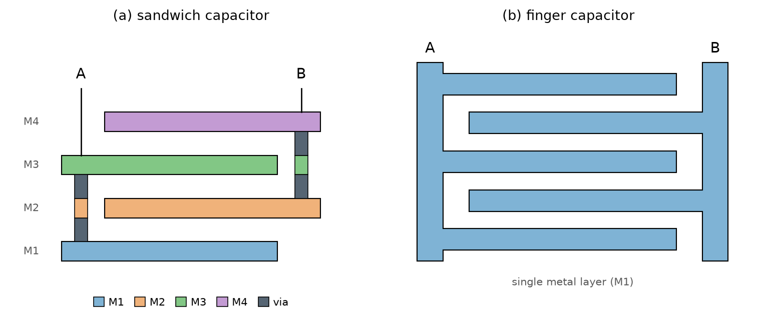
A few additional considerations for capacitors:
- The density of MOM capacitors scales with smaller design rules and the number of metal layers. The lower metal layers should be skipped if the parasitic capacitance to the substrate is a concern.
- The process may offer a specialized metal-insulator-metal (MIM) capacitor (density on the order of fF/µm²) using extra masks and processing steps, offering higher specific capacitance and low parasitics at extra cost.
- For high capacitance density, or where nonlinearity is not critical, the MOSFET gate capacitance can be used, as the gate oxide is tightly controlled in manufacturing.
- In IHP SG13, a MIM capacitor between
Metal5andTopMetal1is available (ca. 1.5 fF/µm²); the MOM finger capacitor has ca. 0.3 fF/µm², so when using 4 metal layers the effective capacitance is comparable to the MIM capacitor.
4.3.5 Diodes
Diodes are formed by the available pn-junctions (\(n^+\) in substrate, \(p^+\) in n-well, n-well in substrate). They are intended mainly for reverse-biased operation, as the forward operation is usually not modeled accurately and should be avoided. Note that forward operation might inject charge into parasitic structures and cause latch-up (see Section 9.2)! Applications of reverse-biased diodes include ESD protection structures, antenna diodes, and varactors.
4.3.6 Bipolar Junction Transistors
High-performance BJTs are available in bipolar and BiCMOS technologies, but at increased wafer cost compared to pure CMOS. In standard CMOS, a parasitic vertical substrate PNP can be implemented (Figure 45): the \(p^+\) diffusion in the n-well forms the emitter, the n-well the base, and the common \(p\)-substrate the collector. The performance is limited (\(\beta \approx 1 \ldots 10\)), and the collector is tied to the substrate potential. Such a structure is mainly used in bandgap reference circuits where collector and base are shorted to \(V_\mathrm{SS}\) (ground), and the foundry usually supplies a fixed layout template that shall not be modified.
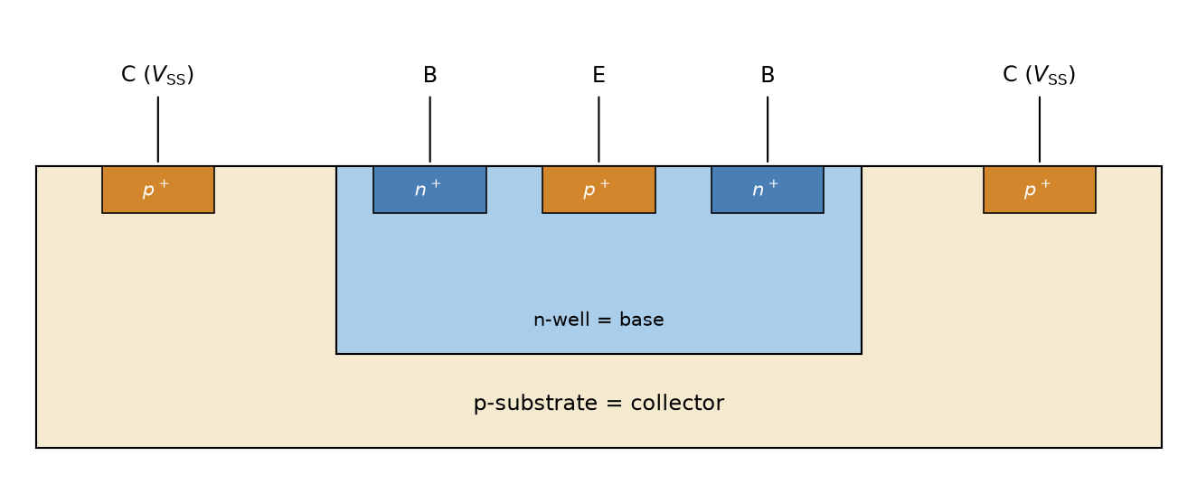
4.4 Design Rules
The design rules (DRs) are the interface between the mask designer (layout engineer) and the foundry. Complying with the layout design rules ensures manufacturability with a high yield:
- The design rules are provided as a specification document and as a run set for layout verification tools (e.g., KLayout, Magic, Cadence Pegasus, or Siemens Calibre).
- The rules are either given in relative dimensions (“lambda rules”) for easy scaling, or in absolute dimensions (“micron rules”).
- Modern CMOS technologies typically involve several hundred to thousands of layout design rules.
- Consider the relatively large spacing rule between
RXandNW: it pays off to group PMOS and NMOS transistors together, respectively!
The four basic geometric rule types—minimum width, minimum spacing, minimum enclosure, and minimum extension—are illustrated in Figure 46.
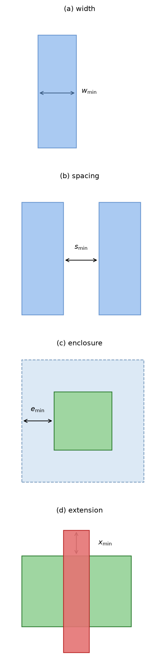
RX in NW), and (d) minimum extension of one shape beyond another (e.g., the poly endcap over RX).
4.4.1 Density Rules
Density rules require a minimum and a maximum layer density within a specified area; this is needed to avoid over-polishing during CMP and to achieve uniform etch rates. For example, M1 might require 30 % minimum and 70 % maximum fill in any 1 mm × 1 mm window. For digital chips, density rules are satisfied automatically by fill programs. For analog chips, layout engineers have to add dummy structures manually (effort!) or with a fill program after the layout is finished; note that fill structures can cause asymmetries or reduced quality factor in inductors. Metal fill can also be put to good use as a ground plane.
4.4.2 Antenna Rules
If a metal interconnect with a large area is tied to the small gate of a MOSFET, the metal area acts as an “antenna” during plasma etching: it collects ions and can rise to a high potential, and the gate oxide may break down! The remedies, shown in Figure 47, are either a discontinuity in the charge-collecting metal (routing briefly through a higher metal layer, which is patterned only after the lower layer has been etched) or an antenna diode connected to the gate node (the processing is done at high temperatures, where the diode is quite conductive in either polarity, harmlessly draining the collected charge).
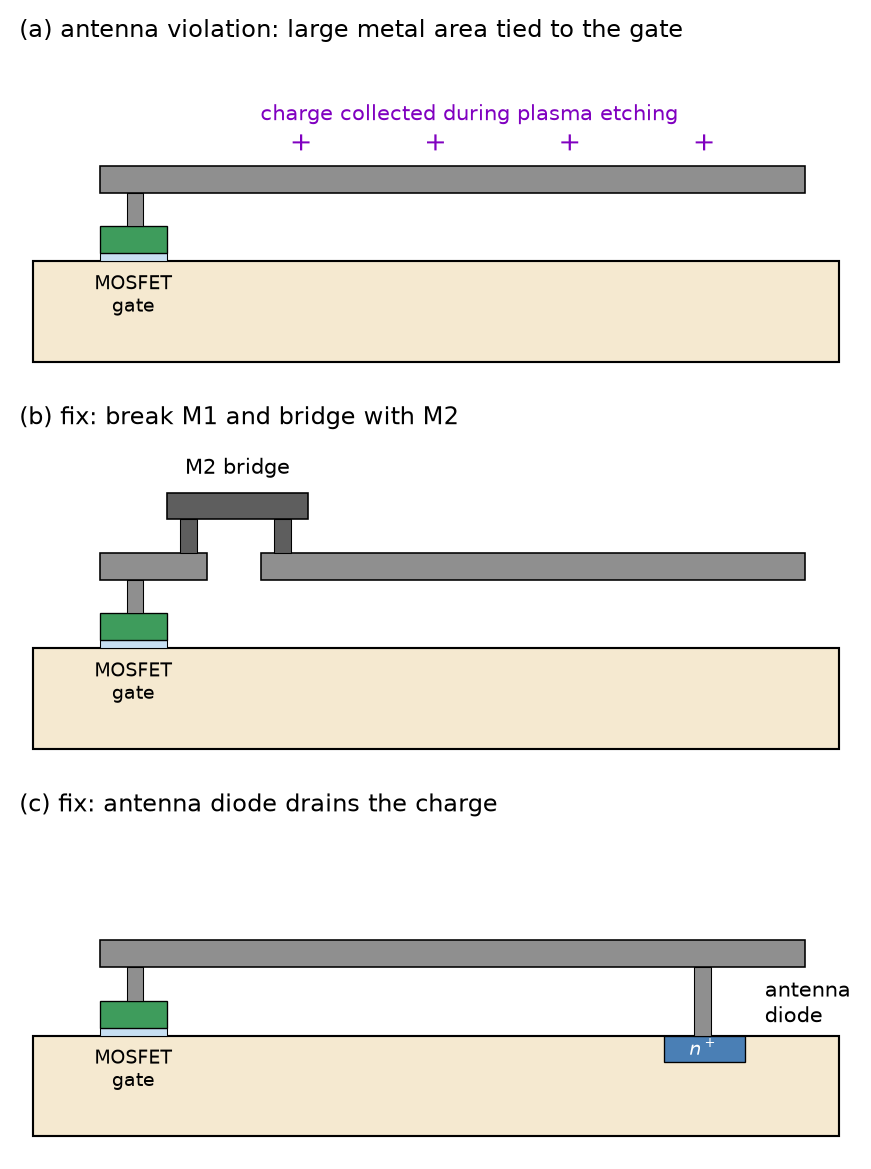
M1 wire connected to a gate collects charge during plasma etching and can destroy the gate oxide; (b) breaking the M1 wire and bridging with M2 limits the charge collected while M1 is etched; (c) an antenna diode drains the collected charge harmlessly into the substrate.
The complete layout rules of the open-source IHP SG13 PDK can be found in the SG13G2 layout rules document and serve as a practical example of a production DRC rule set.
4.5 Analog Layout Techniques
Analog circuits, unlike digital ICs, do not primarily aim to maximize density, but demand the minimization of effects such as crosstalk, mismatch, and noise. Useful techniques are multi-finger transistors, matching and symmetry, and careful floor planning; further treatments of analog layout can be found in (Razavi 2017; Allen and Holberg 2012), and an exemplary analog IC design employing these techniques is described in (Schmickl et al. 2020).
4.5.1 Multi-Finger Transistors
A transistor with a large \(W\) should be split into multiple parallel devices (“fingers”) to make the layout structure compact, as shown in Figure 48. This splitting also reduces the gate resistance (see Equation 32; for RF, keep the resistance of each gate finger below \(1/g_\mathrm{m}\)) and can lower the junction capacitance at the drain or source, since neighboring fingers share their diffusion regions.
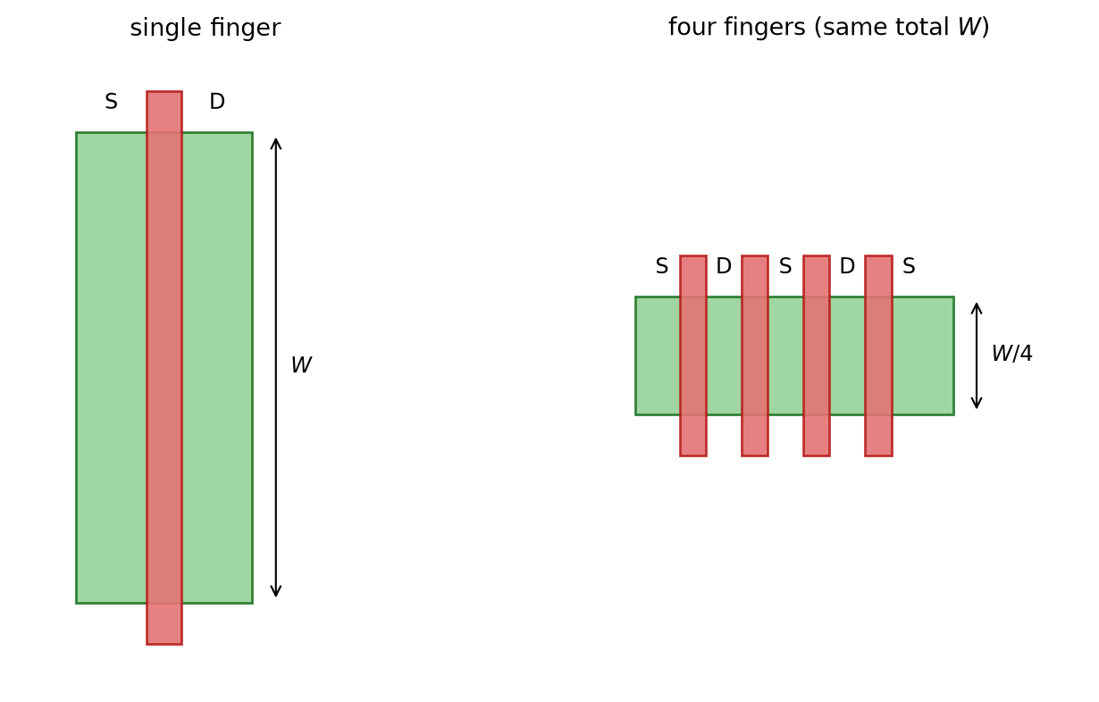
The layout of a cascode circuit (or any series connection of MOSFETs, e.g., in NAND/NOR gates) can be simplified if the stacked devices have equal widths: the drain of the bottom device and the source of the top device can then share the same diffusion region, which is small because it needs no contacts, as shown in Figure 49.
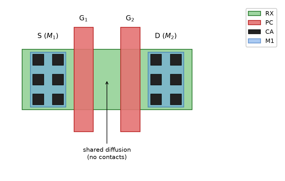
4.5.2 Matching
Asymmetries lead to mismatch, which introduces input-referred offsets and limits the minimum processable signal level; common-mode and power-supply rejection are degraded as well. Good matching of integrated devices can only be achieved if the following conditions are met:
- The devices are constructed from identical unit devices: a MOSFET with width \(4W\) matches a transistor with width \(2W\) only if both are constructed from unit transistors of equal width (and equal \(L\)—remember that \(V_\mathrm{th}= f(L)\) due to SCE/RSCE)!
- The devices are oriented in the same direction, and the current flow in all matched devices has the same direction—avoid mirroring or “snaking”!
- The devices are surrounded by similar structures; to achieve this for edge devices, spend dummy elements (see Figure 50).
- To combat process gradients, place the matched devices on the symmetry line of the gradient (if known), or use common-centroid arrangements (see Figure 52).
- For ac symmetry, consider the wiring of \(R\) and \(C\), and make the wiring parasitics as symmetrical as possible.
- Consider secondary effects: gate shadowing (implant variation due to topographical differences and tilted implant angle), mechanical stress from shallow-trench isolation, and non-uniform doping due to the well-proximity effect (dopants scattering off the well-mask edges cause doping variations, especially impacting PMOS).
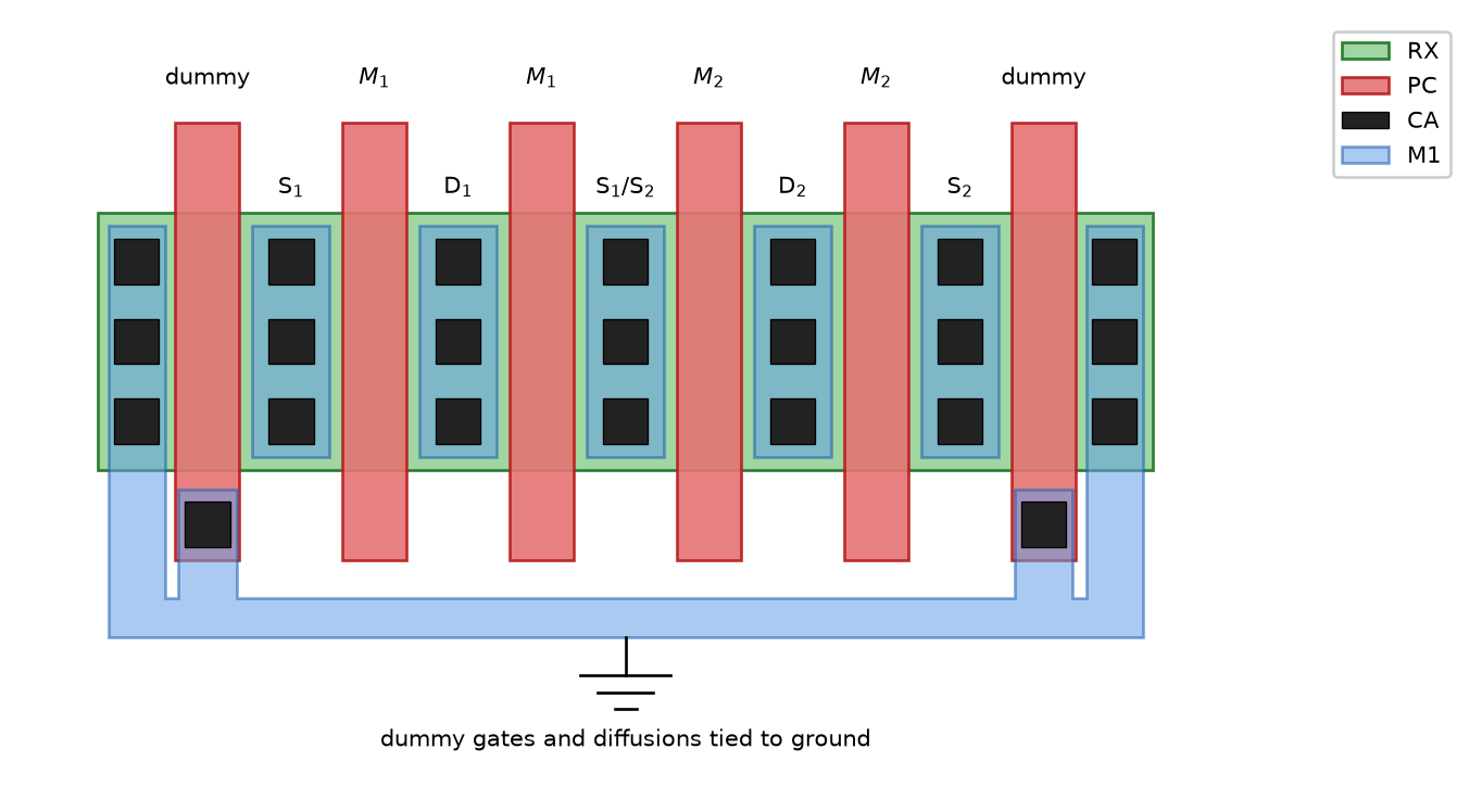
The same reasoning applies to passive devices. Figure 51 shows an array of four matched unit resistors: identical width and length, identical orientation, and a constant pitch, so that \(R_1\) and \(R_4\) at the edges see the same surroundings as \(R_2\) and \(R_3\) in the middle. Note that the dummy strips are not left floating, but are shorted and tied to ground to keep them at a defined potential.
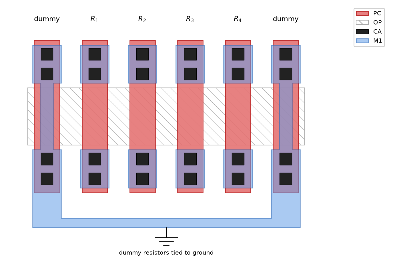
OP runs across the whole array so that every resistor body sees the same edge. A dummy strip at each end gives the outer resistors the same neighborhood as the inner ones. The dummies are shorted by metal and tied to ground, so they sit at a defined potential instead of floating.
Gradients across a die can be caused by doping and film-thickness variations (well approximated by a linear gradient for devices in proximity), by temperature gradients originating from areas with large power dissipation, and by mechanical stress from packaging or metallization (avoid low-level metal routing over sensitive devices). A common-centroid arrangement cancels linear gradients to first order, as shown in Figure 52: each component is decomposed into two or more parts that are placed diagonally opposite each other, so that all component centroids coincide.
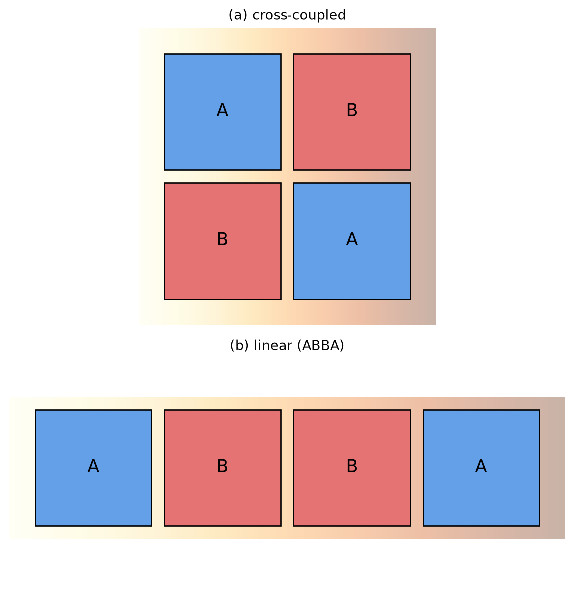
The same principle applies to capacitors: Figure 53 shows a matched capacitor pair with a ratio of \(C_1 = 8 C_2\), realized from identical unit capacitors with a common centroid and surrounded by dummy capacitors. If \(C_1\) and \(C_2\) are used, e.g., in a switched-capacitor amplifier, the voltage gain can be precisely set to \(A_\mathrm{v} = C_1 / C_2 = 8\).
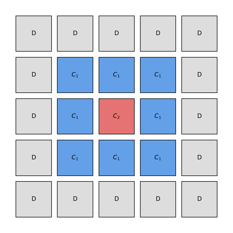
4.5.3 Floor Planning
Floor planning is an important task when constructing the overall IC layout. Things to consider are:
- Locations of pins and interfaces; distribution of \(V_\mathrm{DD}\) and \(V_\mathrm{SS}\) pins; isolation of sensitive I/O signals.
- Cell sizes and aspect ratios (allowing an area-efficient placement of the macros).
- Isolation between different circuit blocks (e.g., keep sensitive analog blocks away from noisy digital blocks).
- Power and clock distribution; wiring channels for signal buses.
- The package type used (wire-bond or flip-chip).
A common mistake: a great job laying out lots of cells, then running out of time, resulting in a big mess when placing and connecting them—start with a top-down plan!
4.6 Additional Layout and Mask Structures
In addition to the final chip layout, further structures are placed on the masks (usually by the wafer fab):
- Seal ring: The seal ring runs along the circumference of the chip and seals the singulated die against moisture and other contamination. It also acts as a crack-stop, protecting the inner die from cracks formed while sawing the wafer into individual dice. Since the seal ring forms a closed metal loop around the chip, crosstalk considerations may suggest connecting it to a dedicated pin.
- Scribe line (kerf): This is where the chip is cut with a diamond saw or a laser.
- Alignment marks: Used to align the different masks during processing.
- Critical-dimension structures: Measured after processing to verify proper polysilicon or metal etching, enabling closed-loop process control.
- Vernier structures (“Nonius”): Closely spaced parallel lines on two different layers that allow judging the inter-layer alignment.
- Test structures: Chains of contacts and vias, as well as test transistors, are used to evaluate contact resistance, transistor parameters, and other important process parameters. They are usually placed in the scribe lines or on dedicated process control monitor (PCM) test chips; the PCM measurement reports can often be obtained from the foundry.
4.7 Layout Checks
Three automated checks safeguard the layout before tapeout:
- DRC (design rule check): a program/run set that automatically checks the layout data for compliance with the design rules of the wafer fab. All flagged errors must be corrected; otherwise, manufacturing issues can occur.
- LVS (layout versus schematic): a netlist extracted from the layout data is compared against the schematic netlist, checking connectivity of signals and power as well as device sizes (\(W\) and \(L\) of transistors, dimensions of \(R\) and \(C\)). Usually, all flagged errors must be corrected.
- ERC (electrical rule check): additional checks not covered by DRC or LVS, such as floating MOSFET gates, floating wells, or antenna rules. Sometimes common mistakes (e.g., high-resistance connections) are covered in the ERC run set and checked automatically.
4.8 Layout Extraction
The layout implementation has a large effect on the performance of the final circuit:
- Wiring adds delays (\(R\), \(L\), \(C\)) and coupling (\(k\), \(C\)) to the circuits.
- Layout-dependent effects (LDE), like well proximity, can only be modeled with information about the actual layout of the devices and their surroundings.
- Substrate effects (like crosstalk) can only be extracted from the actual placement.
Considering layout effects in simulation is paramount and usually requires iteration between circuit design and layout: circuit design and simulation → layout creation → parasitic extraction → re-simulation → circuit and/or layout refinement → repeat. In the digital flow, wiring delays extracted from the layout are added to the gate-level netlist for timing analysis, and voltage drops in the power network (\(V_\mathrm{DD}\)/\(V_\mathrm{SS}\) droop and ripple) are extracted and considered as additional timing derating. For analog and high-performance circuits, simulation including layout parasitics is mandatory to guarantee the performance and functionality of the fabricated circuit!
Different levels of extraction realism trade off accuracy against simulation speed:
- C-decoupled: The parasitic capacitance of each node’s wiring is added as a lumped capacitor to ground. There is almost no impact on simulation speed (no new nodes are introduced), but no crosstalk between nodes is captured. This extraction can be used on fairly large circuits to add a first level of realism.
- C-coupled: Parasitic capacitances to the substrate and between nodes are added; capacitive crosstalk is modeled, but no inductive effects. Moderate impact on simulation speed (more elements in the circuit matrix).
- RC-extracted: Parasitic \(R\) and \(C\) of the wiring are extracted and added to the netlist, yielding a realistic model of performance and crosstalk without inductive effects. This has a large impact on simulation speed, as many new nodes are introduced; this mode should be used for circuit blocks of moderate complexity.
- RLCK-extracted: Parasitic \(R\), \(C\), \(L\), and \(k\) of the wiring are extracted, resulting in a very accurate simulation including the main crosstalk effects—but the circuit network gets much larger, impacting simulation time and convergence.
- EM simulation: Highest accuracy; the resulting \(S\)-parameters are either used directly in frequency-domain simulations or transformed into equivalent lumped-element circuits. Huge simulation-time impact, but valid to very high frequencies (> 100 GHz); usually only suitable for individual circuit blocks.
NoteParasitic Extraction with KLayout-PEX
Our open-source parasitic extraction tool KLayout-PEX (invoked as kpex) implements several of these extraction levels for KLayout, using different engines (an analytical 2.5D engine, a wrapper around MAGIC, and the FasterCap 3D field solver) that trade off speed against accuracy. Supported PDKs include IHP SG13G2 and SkyWater sky130A. Further information can be found in the online documentation.
5 IC Packaging
The finished wafer is not yet a usable product: the individual dice have to be separated, connected, and protected. This chapter covers the path from the processed wafer to the packaged integrated circuit, the most important package families, thermal design, and the electrical parasitics that packages introduce.
5.1 From Wafer to Packaged IC
After wafer processing (see Section 3), the wafer is usually first thinned by grinding from the backside, depending on the package technology (typical final thickness 100 to 300 µm). After thinning, the wafer is mounted on a carrier tape and split into individual dice—this process is called dicing. A saw blade is the standard tool; alternatively, a laser can be used to (pre-)cut the wafer. An exception is the wafer-level package (WLP), where the wafer is further processed before sawing.
The IC package then provides the following important functions:
- Electrical connection of signals and power from the IC to the PCB.
- Interconnects adding little delay or distortion (small parasitic \(R\), \(L\), \(C\), and \(k\)).
- Mechanical connection of the IC to the PCB.
- Removal of the heat produced in the IC.
- Protection of the IC from mechanical damage and the environment.
- Compatibility with the thermal expansion (CTE) of the PCB.
- Inexpensive manufacturing and testing.
5.2 Chip-to-Package Connection
Traditionally, an IC is surrounded by a pad frame: metal pads on a pitch of 80 to 200 µm along the die circumference. Bond wires attach the pads to the package, a lead frame distributes the signals within the package, and a metal heat spreader (paddle) helps with cooling. In flip-chip packages or WLPs, the pads can instead be distributed arbitrarily across the die area (close to the relevant circuit blocks). Figure 54 shows the wire-bond arrangement.
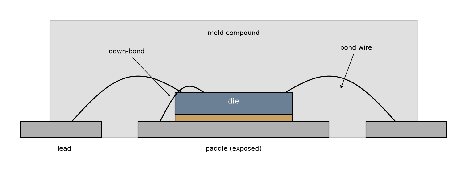
A few notes on the bond pads themselves:
- A simple pad consisting only of a square of top metal may “lift off” during bonding due to insufficient adherence; a mechanically robust pad is formed from the two topmost metal layers, connected by many small vias, at the price of somewhat larger capacitance.
- Pads carrying RF signals can be shaped as octagons to reduce their capacitance (about 20 % reduction).
- In some processes, it is allowed to place circuitry (e.g., ESD protection) below the pads to save chip area—called pad-over-active-area (PoAA).
5.3 Package Types
Simple lead-frame-based packages using bond wires are cost-effective but have a limited number of I/Os, and the bond wires cause parasitic inductance and mutual (inductive and capacitive) coupling. Laminate-based packages can have several signal and power layers (2–4), like tiny PCBs; they are based either on bond wires or on flip-chip assembly:
- Pads can be placed across the whole surface of the die rather than only at the periphery.
- The top-level metal pads are covered with solder balls.
- The IC is mounted upside down and must be carefully aligned to the package (done blind!); then heat is applied to melt the solder balls.
- This process is also called controlled collapse chip connection (C4).
Figure 55 shows cross sections of the most important package families.
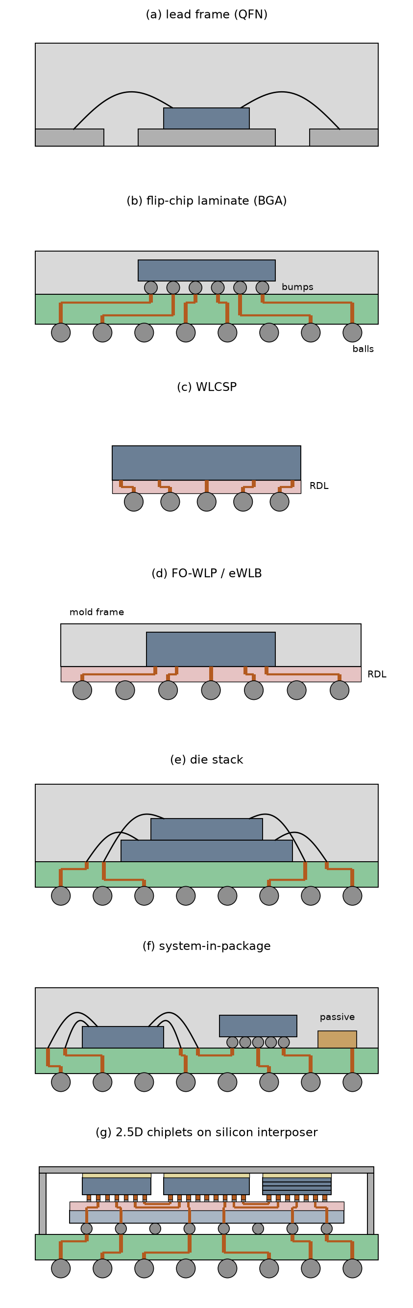
5.3.1 Lead-Frame Package
A lead-frame package is available with or without leads (e.g., QFP with gull-wing leads versus leadless QFN). The die is glued to the lead-frame paddle and bonded to the leads using Au, Al, Cu, or Ag wires; a “down-bond” to the paddle is usually possible and provides low inductance due to the short wire. The whole assembly is covered and protected by an epoxy mold compound. The lead-frame paddle can be exposed and soldered to the PCB for best grounding and thermal performance.
5.3.2 Laminate Package
A laminate package can be seen as a small PCB with fine design rules; the die is either wire-bonded (cheaper) or soldered face-down using solder bumps (C4) or Cu pillars (better electrical performance). The connection to the main PCB is made with solder balls (BGA), pins, or exposed lands. The mold compound protects the assembly; for flip-chip assembly it can be omitted and potentially replaced by a metallic heat spreader.
5.3.3 Chip-Scale and Wafer-Level Packages
The wafer-level package (WLP) offers very low cost, excellent electrical properties, and the smallest possible size (package size = die size), but provides little protection of the die. The processing happens on the wafer level: a redistribution layer (RDL) re-routes the pads, solder balls are applied, and only then are the dice singulated. If the I/O count is too large to fit onto the die area, a fan-out WLP (FO-WLP/eWLB) can be used, where the die is extended in size by a mold frame: the dice are first singulated, then re-assembled on an artificial wafer where the surrounding area is filled with mold compound, and then processed like a WLP.
5.3.4 Stacked Packages
For dense systems, several dice can be combined in one package: as a die stack (dice stacked on top of each other, connected by bond wires or through-silicon vias), as package-on-package (PoP) (e.g., a memory package soldered on top of a processor package), or as a system-in-package (SiP), where several dice and passives are integrated on a common laminate substrate.
5.3.5 2.5D Integration with Chiplets and Silicon Interposer
High-end systems like GPUs, AI accelerators, and server processors increasingly split a large SoC into several smaller dice, called chiplets, which are placed side by side on a silicon interposer (Figure 55 (g)); a well-known example is TSMC’s CoWoS (chip-on-wafer-on-substrate). This approach is motivated by several factors:
- A single monolithic die is limited by the reticle size of the lithography tool, and the yield drops rapidly with die area; several smaller dice yield better and can exceed the reticle limit in total.
- Each chiplet can be fabricated in the most suitable technology (heterogeneous integration), e.g., the compute logic in a leading-edge node, while I/O, analog, or RF functions stay in a mature, cheaper node.
- Memory can be placed very close to the processor; a typical example is high-bandwidth memory (HBM), a stack of DRAM dice connected by through-silicon vias.
- Proven chiplets can be reused across products, reducing design effort.
The interposer is a passive silicon die (or a large part of a wafer) that is fabricated with a back-end-of-line process. Its fine-pitch wiring (line width and spacing in the µm range) allows thousands of short, dense connections between the chiplets, which is not possible with laminate substrates. The chiplets are flipped and attached to the interposer with Cu pillars with a thin solder cap (sometimes called microbumps, pitch typically 40 to 50 µm). Through-silicon vias (TSVs) lead the supply and external signals through the thinned interposer (thickness ca. 100 µm) to C4 bumps (pitch ca. 150 µm), which connect the interposer to a laminate substrate. The laminate then fans out to the BGA balls, just like a regular flip-chip package. Instead of a mold compound, such packages are typically covered by a metal lid, which is attached to the backside of the chiplets with a thermal interface material (TIM) and acts as a heat spreader.
As the pitch grows by roughly an order of magnitude at each level (chiplet, interposer, laminate, PCB), this arrangement is a hierarchy of increasingly coarse wiring. Several variants exist to reduce cost: an organic RDL interposer instead of silicon, or small silicon bridges embedded in the laminate only below the chiplet edges (e.g., Intel EMIB). In 3D integration, chiplets are stacked directly on top of each other using TSVs and hybrid bonding (Cu-to-Cu bonding without solder, pitch below 10 µm).
Designing chiplet-based systems brings new challenges: the die-to-die interfaces need to be standardized to allow combining chiplets from different sources (e.g., UCIe, Universal Chiplet Interconnect Express), each chiplet must be tested before assembly (known-good die, as a single faulty chiplet ruins the whole expensive package), power delivery and heat removal must be co-designed with the package, and the mechanical stress and warpage of the large assembly must be controlled.
5.4 Thermal Design
Managing the die temperature is an important aspect of package selection. Depending on the application, different ambient temperature ranges apply, which result in different on-die temperature ranges (due to the self-heating of the die caused by its power dissipation):
- Consumer ambient temperature range: −30 to +85 °C.
- Industrial/automotive ambient temperature range: −40 to +85 °C.
- Usual IC technology junction temperature limits: −40 to +125 °C.
- Automotive IC junction temperature limits: −40 to +150 °C.
5.4.1 Thermal Calculations
Thermal calculations behave analogously to Ohm’s law, as thermal paths can be modeled as series or parallel connections, using these equivalences: temperature difference \(\Delta T \mathrel{\hat{=}}\) voltage \(V\), heat flow \(Q \mathrel{\hat{=}}\) current \(I\), thermal resistance \(R_\mathrm{th} \mathrel{\hat{=}}\) resistance \(R\):
\[ \Delta T = Q \cdot R_\mathrm{th} \tag{49}\]
\[ R_\mathrm{th,series} = \sum_{i} R_{\mathrm{th},i} \qquad \frac{1}{R_\mathrm{th,parallel}} = \sum_{i} \frac{1}{R_{\mathrm{th},i}} \tag{50}\]
An important property of an IC package is its ability to transport the heat generated on the die to the outside, limiting the die’s self-heating. This property is the thermal resistance, usually a function of the package, the die, and the PCB design. Using
\[ \Delta T = R_\mathrm{th,ja} \cdot P_\mathrm{diss} \tag{51}\]
with \(\Delta T\) the on-chip temperature rise versus the ambient temperature in K, \(R_\mathrm{th,ja}\) the junction-to-ambient thermal resistance in K/W, and \(P_\mathrm{diss}\) the on-chip power dissipation in W, the die temperature can be estimated. A typical \(R_\mathrm{th,ja}\) value is provided by the package manufacturer; for high accuracy, a thermal simulation has to be performed. Strictly speaking, \(R_\mathrm{th,ja}\) is defined for a specific PCB design and environment (standardized in, e.g., JEDEC JESD51) and needs re-evaluation for specific cases (PCB size, number of layers, copper and via density, casing, airflow, etc.). Figure 56 shows how a complete thermal path is modeled as a resistor network.
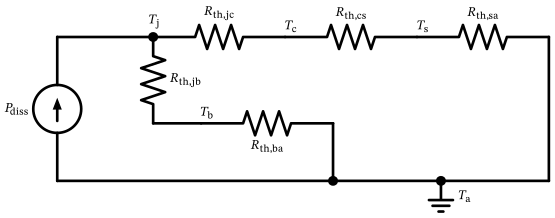
5.5 Package Parasitics
The parasitics associated with the package and the connections to the chip introduce difficulties in high-speed or high-accuracy designs: trace self-inductance, mutual inductance, and capacitance limit the achievable performance. Packaging continues to limit the performance of high-end designs, which is why advanced packages like WLCSP with minimal \(L\) and \(C\) are used for high-performance ICs. Figure 57 shows the equivalent circuit of a single package connection.
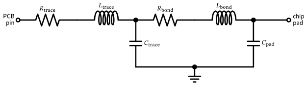
Simple approximations for the inductance of common package geometries are given below (higher accuracy requires EM simulation; the underlying transmission-line theory is covered in (Pozar 2011)). For a round wire at height \(h\) above a ground plane (wire radius \(r\)):
\[ L' \approx 0.2 \ln \left( \frac{2h}{r} \right) \; \mathrm{nH/mm} \tag{52}\]
For a flat trace of width \(W\) at height \(d\) above a ground plane:
\[ L' \approx \frac{1.6}{0.72 + W/d} \; \mathrm{nH/mm} \tag{53}\]
The mutual inductance of two round wires at distance \(d\) and height \(h\) above the ground plane:
\[ L_\mathrm{m}' \approx 0.1 \ln \left[ 1 + \left( \frac{2h}{d} \right)^2 \right] \; \mathrm{nH/mm} \tag{54}\]
A typical bond wire has a radius of 12.5 µm and larger, and an inductance of roughly 1 nH/mm.
Note 4: Example Calculation of the Bond-Wire Inductance
Let us assume a bond wire with a diameter of 25 µm (i.e., \(r = 12.5\,\mu\text{m}\)) and a length of \(l = 2\,\text{mm}\), running at a height of \(h = 300\,\mu\text{m}\) above the ground plane. With Equation 52, the inductance per length is
\[ L' \approx 0.2 \ln \left( \frac{2 \cdot 300\,\mu\text{m}}{12.5\,\mu\text{m}} \right) \; \text{nH/mm} = 0.2 \ln (48) \; \text{nH/mm} = 0.77\,\text{nH/mm} \]
and the total inductance of the bond wire is
\[ L = L' \cdot l = 0.77\,\text{nH/mm} \cdot 2\,\text{mm} = 1.55\,\text{nH} \]
Note that the height enters only logarithmically: doubling \(h\) to \(600\,\mu\text{m}\) increases the inductance by just 18 % to \(1.83\,\text{nH}\). At a frequency of \(f = 1\,\text{GHz}\), this bond wire already shows a reactance of
\[ X_L = 2 \pi f L = 9.7\,\Omega \]
If this bond wire carries the supply current of a digital block, a current step of \(\Delta i = 10\,\text{mA}\) within \(\Delta t = 100\,\text{ps}\) causes a supply bounce of
\[ V = L \frac{\Delta i}{\Delta t} = 1.55\,\text{nH} \cdot \frac{10\,\text{mA}}{100\,\text{ps}} = 155\,\text{mV} \]
which is significant for a core supply voltage of about 1.2 V.
To reduce the supply bounce, a second bond wire of the same dimensions is placed in parallel at a distance of \(d = 300\,\mu\text{m}\). With Equation 54, the mutual inductance per length is
\[ L_\mathrm{m}' \approx 0.1 \ln \left[ 1 + \left( \frac{2 \cdot 300\,\mu\text{m}}{300\,\mu\text{m}} \right)^2 \right] \; \text{nH/mm} = 0.1 \ln (5) \; \text{nH/mm} = 0.16\,\text{nH/mm} \]
resulting in a mutual inductance of \(L_\mathrm{m} = L_\mathrm{m}' \cdot l = 0.32\,\text{nH}\) between the two bond wires. The magnetic coupling factor is
\[ k = \frac{L_\mathrm{m}}{\sqrt{L_1 L_2}} = \frac{L_\mathrm{m}}{L} = \frac{0.32\,\text{nH}}{1.55\,\text{nH}} = 0.21 \]
As both bond wires carry currents in the same direction, the mutual inductance adds to the self-inductance of each wire, and the effective inductance of the parallel connection is
\[ L_\mathrm{eff} = \frac{L + L_\mathrm{m}}{2} = \frac{L}{2} (1 + k) = 0.94\,\text{nH} \]
Instead of halving the inductance to \(0.77\,\text{nH}\), the second bond wire reduces it only by 40 %, and the supply bounce for the same current step drops from \(155\,\text{mV}\) to \(94\,\text{mV}\). A larger distance between the bond wires reduces \(k\) and brings \(L_\mathrm{eff}\) closer to \(L/2\). Conversely, if the two bond wires carry unrelated signals, the same coupling causes crosstalk: the current step of \(10\,\text{mA}\) in \(100\,\text{ps}\) in one bond wire induces a voltage of \(L_\mathrm{m} \, \Delta i / \Delta t = 32\,\text{mV}\) in the other.
5.5.1 Multiple Pads, Bond Wires, and Pins
Where a single connection to the chip would sustain a prohibitively large transient voltage drop (\(V = L \, di/dt\)), multiple pads, bond wires, and package pins are used in parallel: \(N\) parallel connections reduce the effective inductance by roughly \(N\) (somewhat less due to the mutual coupling between the parallel wires). This is standard practice for power supplies and high-current outputs.
5.5.2 Exposed Paddle and Down-Bonds
Some packages contain a metal plane (the paddle) to which the die is attached with conductive epoxy. Such packages avoid long, narrow traces in the ground connection: the ground pads are “down-bonded” directly to the paddle, minimizing the inductance, and the paddle is soldered to the board ground. Sometimes the paddle has to be plated in the areas where a down-bond lands, adding cost.
5.5.3 Mutual Inductance and Crosstalk
Supply noise and other disturbances can couple through the mutual inductance (and capacitance) of adjacent bond wires and package traces. The design of the pad frame and the position of the bond wires play a critical role in isolating sensitive connections! Two methods reduce the mutual coupling, illustrated in Figure 58:
- Arrange critical wires perpendicular to each other (mutual inductance requires parallel current paths).
- Interpose \(V_\mathrm{SS}\) or \(V_\mathrm{DD}\) wires between critical bond wires; the return current in the interposed wire partially cancels the coupled flux.
Mutual inductance can even be used to advantage: routing a supply and its return current in adjacent, parallel bond wires carrying opposite currents reduces the effective loop inductance.
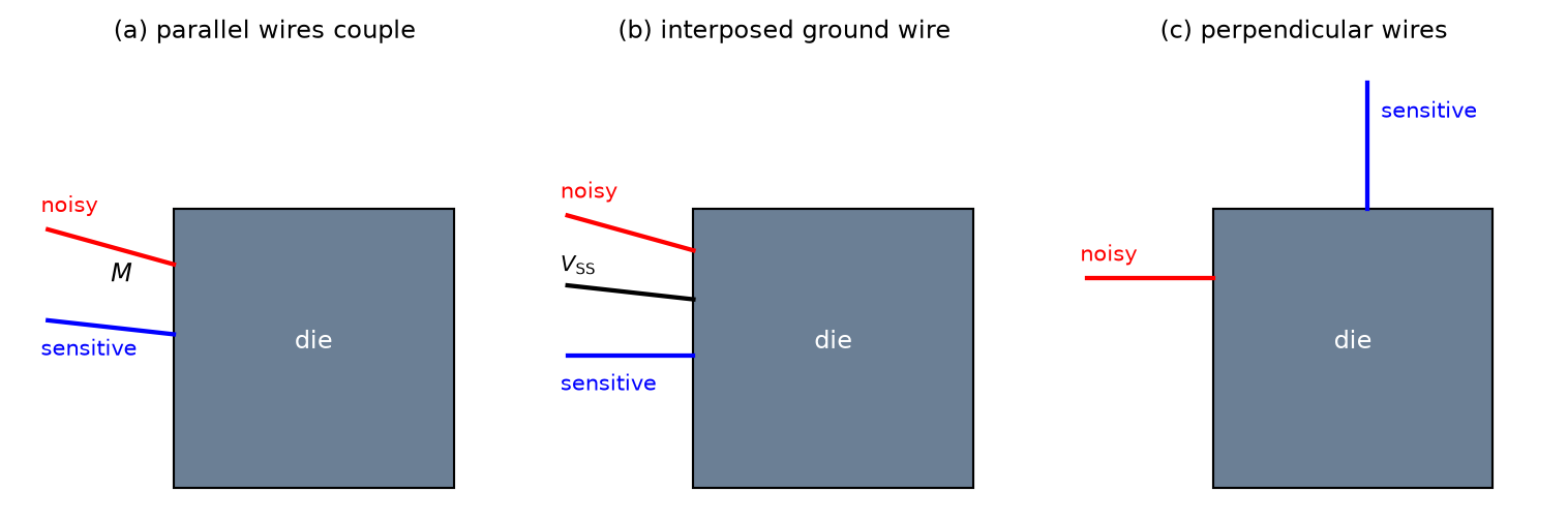
5.5.4 Bond Wires as Circuit Elements
Since a bond wire is a relatively high-\(Q\) inductor (inductance ca. 1 nH/mm, low resistivity of Au or Al), some designs use it as a circuit element, e.g., in high-frequency \(LC\) oscillators (Craninckx and Steyaert 1995). However, the mechanical tolerances of the bond-wire geometry translate into inductance tolerance, which must be taken into account. More generally, any conducting structure in a package can be used to form inductors, capacitors, or even antennas (e.g., in CSP or laminate packages).
5.6 Package Qualification
In addition to the qualification of the silicon technology (see Section 3.10), the package must be qualified to prove that the assembly of die, bond wires or bumps, substrate, and mold compound survives soldering, handling, and the thermal and environmental stress of its application over the intended lifetime. The framework is again set by JEDEC JESD47, and for automotive products by AEC-Q100, which groups these tests as accelerated environment stress tests and package assembly integrity tests. As for the silicon, a typical sample consists of three assembly lots of 77 parts per test, and zero failures are accepted. Table 10 lists typical tests.
| Test (examples) | Standard | Motivation & check |
|---|---|---|
| Pre-conditioning (PC) | JESD22-A113 | Moisture soak and reflow simulate storage and board assembly before the other stress tests. |
| Moisture sensitivity level (MSL) | J-STD-020 | Classification of how long a package may be exposed to ambient moisture before soldering. |
| Temperature cycling (TC) | JESD22-A104 | Repeated heating and cooling must not cause failures (thermal expansion mismatch, see CTE). |
| Temperature humidity bias (THB) / biased HAST | JESD22-A101 / A110 | Corrosion and leakage under humidity, temperature, and applied voltage. |
| Unbiased highly accelerated stress test (UHAST) | JESD22-A118 | Exposure of package and die to high temperature and humidity without bias. |
| High-temperature storage life (HTSL) | JESD22-A103 | Storage at high temperature for thousands of hours (intermetallic growth). |
| Wire bond pull and shear | MIL-STD-883 (2011) / JESD22-B116 | Mechanical strength of the bond wires and their connections. |
| Solder ball shear | JESD22-B117 | Mechanical strength of the solder balls of BGA and WLCSP packages. |
| Drop test | JESD22-B111 | The assembled PCB is dropped repeatedly under standardized conditions. |
| Temperature cycling on board (TCoB) | IPC-9701 | The assembled PCB is temperature-cycled to check the solder-joint reliability. |
These tests fall into three groups: component-level stress tests (PC, TC, THB/HAST, UHAST, HTSL) that accelerate the degradation of the package, assembly integrity tests that check the mechanical quality of the interconnects directly, and board-level tests (drop, TCoB) that stress the solder joints between package and PCB. After each stress test, the parts are electrically tested against the datasheet at the read points; in addition, non-destructive inspection like scanning acoustic microscopy (C-SAM) reveals delamination and cracks inside the package, and X-ray imaging shows deformed bond wires. Failing parts are analyzed further, e.g., by cross-sectioning.
Pre-conditioning (PC) is not a test on its own but the mandatory first step before TC, THB/HAST, and UHAST. The mold compound and the laminate are polymers that absorb moisture from the ambient air during storage. When the package is then soldered to the PCB, it is heated within seconds to a peak temperature of up to 260 °C for lead-free solder, and the absorbed water evaporates explosively. The vapor pressure can delaminate the mold compound from the die or the lead frame, crack the package, or break bond wires—the so-called popcorn effect. Pre-conditioning therefore reproduces the life of a part before it reaches the application: a bake to dry the parts, a moisture soak according to the targeted MSL, and three reflow cycles to simulate board assembly including a rework.
The moisture sensitivity level (MSL) is determined according to J-STD-020 and states how long a package may be exposed to a factory environment (≤30 °C, 60 % RH) after opening its dry pack before it must be soldered. It ranges from MSL 1 (unlimited floor life, soaked at 85 °C and 85 % RH for 168 h) and MSL 3 (floor life of 168 h, a common target for plastic packages) to MSL 6 (parts must be baked right before soldering). Packages with MSL 2 and higher are shipped in sealed moisture-barrier bags with desiccant, and parts that exceeded their floor life have to be baked before use (J-STD-033).
Temperature cycling (TC) addresses the thermo-mechanical stress caused by the different coefficients of thermal expansion (CTE) of the package materials: silicon expands by about 2.6 ppm/K, the copper lead frame by about 17 ppm/K, the laminate by about 14 to 17 ppm/K, and the mold compound by roughly 8 to 15 ppm/K (below its glass transition temperature). Every temperature change therefore causes shear stress at the interfaces. The parts are cycled between typically −55 °C and +125 °C (or −40 °C and +150 °C for automotive), with several hundred to 1000 cycles. Typical failure mechanisms are cracked wire-bond heels, lifted ball bonds, delamination, cracked dice or passivation layers, and fatigue of flip-chip bumps (which is why flip-chip dice are usually underfilled). The acceleration factor to the milder temperature swings of the application follows the empirical Coffin–Manson relation, where the number of cycles to failure scales with a power of the temperature swing.
Temperature humidity bias (THB) and its accelerated variant, biased HAST, combine moisture with an electric field. In the classic 85/85 test, the parts are operated for 1000 h at 85 °C and 85 % RH with a static bias applied to the pins; HAST reaches a similar stress in about 96 h at 130 °C and 85 % RH in a pressurized chamber. Moisture diffuses through the mold compound and along interfaces to the die surface, where it dissolves ionic contaminations (e.g., chlorine from the mold compound); together with the applied voltage this causes electrochemical corrosion of the Al bond pads and metal lines, or leakage currents between adjacent pins. A dense passivation layer and a well-adhering mold compound are the main countermeasures. Unbiased HAST (UHAST) applies the same humidity stress without bias (typically 96 h at 130 °C and 85 % RH), which isolates the purely chemical and mechanical effects of moisture, like galvanic corrosion between dissimilar metals and delamination.
High-temperature storage life (HTSL) stores unbiased parts at typically 150 °C for 1000 h. Its main target is the bond interface between the wire and the Al pad: gold and aluminum form intermetallic compounds whose growth is thermally activated. Uneven diffusion of the two metals creates voids (Kirkendall voiding), which increase the contact resistance and weaken the bond until it lifts off; the purple color of one of these compounds (AuAl2) gave this failure the name “purple plague.” Copper wires, which have widely replaced gold for cost reasons, form Cu–Al intermetallics much more slowly, but they are more sensitive to corrosion in the humidity tests. As for HTOL, an Arrhenius acceleration factor relates the storage test to the application temperature.
Wire bond pull and shear tests and solder ball shear tests are destructive mechanical tests of the interconnects themselves. In the pull test, a hook is placed below the bond wire and pulled upward until the wire breaks; both the force and the location of the break are recorded—a break in the wire is acceptable, while a lifted bond indicates a weak connection. In the shear test, a tool pushes the ball bond or the solder ball sideways off its pad. These tests are performed on a small sample per assembly lot and are also used for monitoring the ongoing production.
Board-level reliability tests assess the solder joints between package and PCB, which usually fail before the package itself. In the drop test, a standardized JEDEC test board with the mounted components is subjected to repeated mechanical shocks (e.g., 1500 g for 0.5 ms) while the daisy-chained solder joints are monitored for interruptions; this test is essential for handheld devices. In temperature cycling on board (TCoB), the assembled board is cycled (e.g., between 0 °C and 100 °C) until the solder joints fail by fatigue. The CTE mismatch between silicon and the PCB is particularly critical for WLCSPs, where the silicon die is soldered directly to the board, and for large BGAs, where the distance to the neutral point of expansion is large; the achievable number of cycles therefore limits the maximum die size of a WLCSP.
A qualified package is not qualified forever. As a package family covers many die sizes and pin counts, qualification is usually performed on worst-case representatives (e.g., the largest die in the thinnest package), and other products are qualified by similarity. Any significant change of the materials (mold compound, wire material, die attach), the assembly site, or the process requires a requalification and a formal notification of the customers (JESD46).
6 Testing
Integrated circuits must be tested for functionality and specification compliance before they are shipped. Defects introduced during manufacturing, as well as parameter variations, are unavoidable—not every IC on a wafer is a good device (the yield is below 100 %). Typical defect causes are doping errors and fluctuations, under- or over-etching, misalignment of layers, and contamination by particles. A comprehensive treatment of IC test is given in (Wang et al. 2006); the related field of hardware security and trust is covered in (Bhunia and Tehranipoor 2018).
6.1 Post-Silicon Production Flow
The production flow after wafer manufacturing consists of the following steps:
- Wafer test (optional): bad dice are inked or recorded in the automatic test equipment (ATE) to avoid wasting packages on them. The cost of packaging a bad die has to be weighed against the cost of the wafer test.
- Wafer dicing: the wafer is cut into separate chips, and bad chips are discarded.
- Packaging.
- Final test: ensures that no parts damaged during dicing or packaging are shipped; some parameters might only be testable on the packaged device.
The ATE is typically used in two distinct modes:
- Prototype/characterization testing is very extensive: it looks for worst-case behavior across conditions, establishes guard bands (margins for temperature and measurement uncertainty), is statistically based across hundreds or thousands of engineering samples, and test time is not the main concern.
- Production testing is very time-critical: the tester is expensive, so minimum test time matters; the tests are based on the worst-case conditions established during characterization, and each IC is tested individually.
6.2 Test Equipment
Mixed-signal IC test equipment (manufacturers include Teradyne, Advantest, Cohu, and National Instruments) consists of the parts shown in Figure 59:
- The workstation: the user computer of the test engineer, used for debugging and day-to-day operation of the tester.
- The mainframe: houses the power supplies and measurement instruments and contains the tester computer (including DSP hardware for fast signal analysis).
- The test head: contains the most sensitive measurement electronics, and carries the device interface board (DIB) connecting to the device under test (DUT).
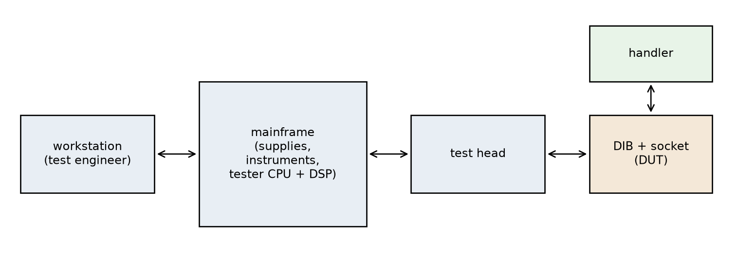
The DIB is a custom-designed PCB that hosts the package socket (for testing packaged ICs) or connects to the probe card (for wafer testing). It also contains interface circuits that cannot be handled by the tester hardware resources (e.g., special components required by the DUT). Contact to the packaged DUT is made with spring-loaded “pogo pins” in the socket. For wafer probing, different probe-card types are used: cantilever probe cards (needles coming in at an angle), vertical (“buckling-beam” or “cobra”) probe cards, and membrane probe cards for high pin counts and fine pitches.
Handlers (robotic pick-and-place or gravity-fed) insert the DUT into the test socket on the DIB. After the test, the ICs are sorted into bins (good = pass, bad = fail, possibly multiple pass grades). The handler can also provide a temperature-controlled environment for hot/cold testing in addition to room-temperature testing (the latter is preferred for cost reasons).
6.3 Mixed-Signal Testing Challenges
- Time is money: A tester plus handler can cost several million dollars, and one second of test time costs 3 to 5 cents. The test program needs a certain time (up to minutes) to cover all relevant functional blocks and critical parameters. Multi-site testing (testing 2/4/8 devices in parallel) reduces the effective test time per device.
- The test socket introduces parasitics (\(R\), \(L\), \(C\)) which impact performance and make precision measurements difficult.
- Accuracy is limited by interference, calibration, and measurement time.
- Repeatability & reproducibility (R&R) are required to obtain the same test results across different testers, DIBs, and test sites.
The classification of measurement errors is summarized in Figure 60: accuracy relates the measurement to the true value (via instrument traceability to standards), while precision splits into repeatability and reproducibility, illustrated in Figure 61.
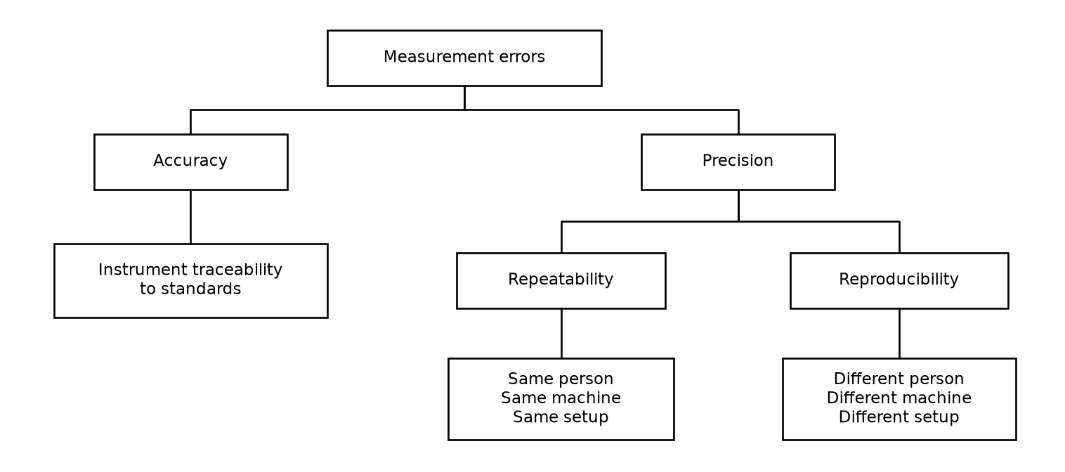
Repeatability is the dispersion of measurements when a quantity is measured several times under the same conditions: same measuring instrument, same parts, same operator, within a short time period. It represents the inherent variation of the measurement system—note that measurements may show good repeatability without being accurate! Reproducibility is the variation between the mean measurements on the same parts when one condition is changed per trial: a different operator, a different instrument, or a different setup.
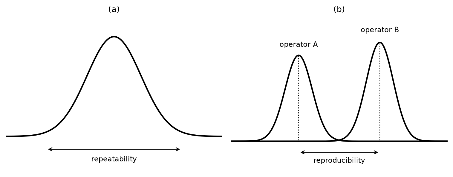
6.4 The Test Plan
The test plan is the governing document for generating the test program and contains:
- Device background information (in addition to the datasheet).
- Special test requirements.
- An explanation of the purpose of each test.
- Assumptions made for particular tests, and why.
- A hardware setup diagram for each test.
- Identification of critical test parameters: not all parameters from the datasheet need to be (or can be) tested in production, due to test time or measurement error; such parameters are guaranteed by design and marked accordingly in the datasheet.
- Binning information: devices might be binned into pass/fail or different pass grades (e.g., by maximum clock frequency). Continuity fails are binned separately, because they could be caused by contact issues of the handler or socket.
6.5 Types of Tests
6.5.1 Continuity Test
The continuity test verifies the contact between the DIB and all pins of the DUT. As essentially all pins have some circuitry connected (at least the ESD protection diodes), a small current is forced into or out of each pin (with a voltage limit to protect the device in case of opens), and the resulting voltage is measured, as sketched in Figure 62:
- A high voltage (running into the voltage limit) means no contact to the IC pin → open.
- A very small voltage means a short is detected at the IC pin → short.
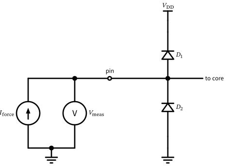
6.5.2 Leakage-Current Test
A non-defective device draws only a small leakage current at the power-supply and I/O pins when in off-mode, so a leakage test is a fast method for detecting failing devices due to shorts and other misprocessing:
- A voltage is applied to all digital and analog inputs, and the current is measured.
- Digital outputs are set to high-Z (if possible), and the leakage current is measured as for the inputs.
- A voltage is applied to the \(V_\mathrm{DD}\) pins and the leakage current is measured; the device must be put into off-mode by applying the proper initialization (reset or power-on sequence).
6.5.3 Memory Test
Memory cells have to be tested for the following fault types caused by production defects:
- Stuck-at faults (stuck-at-0, stuck-at-1) and transition faults (\(0 \rightarrow 1\) or \(1 \rightarrow 0\) not possible).
- Coupling faults (writing to one cell changes the content of another cell).
- Neighborhood pattern-sensitive faults.
Since on-chip memories can be large, memory testing can be costly, requiring a trade-off between fault coverage and test time. Example test methods:
- Zero-one (write all zeros, read all zeros, write all ones, read all ones)—\(\mathcal{O}(n)\).
- Checkerboard (write alternating 0101…, read, write the complement 1010…, read)—\(\mathcal{O}(n)\).
- Walking 1/0 (consecutively fill the memory with ones/zeros and check)—\(\mathcal{O}(n^2)\).
- ROM: read out and compute a checksum/CRC or hash—\(\mathcal{O}(n)\).
Applying these RAM tests can be done by external reads/writes (slow), by the internal CPU (faster), or by dedicated built-in self-test (BIST) hardware (fastest, at the cost of extra silicon area). Figure 63 shows the structure of a RAM BIST: a controller with pattern and address generators exercises the RAM, and a comparator checks the read-back data.
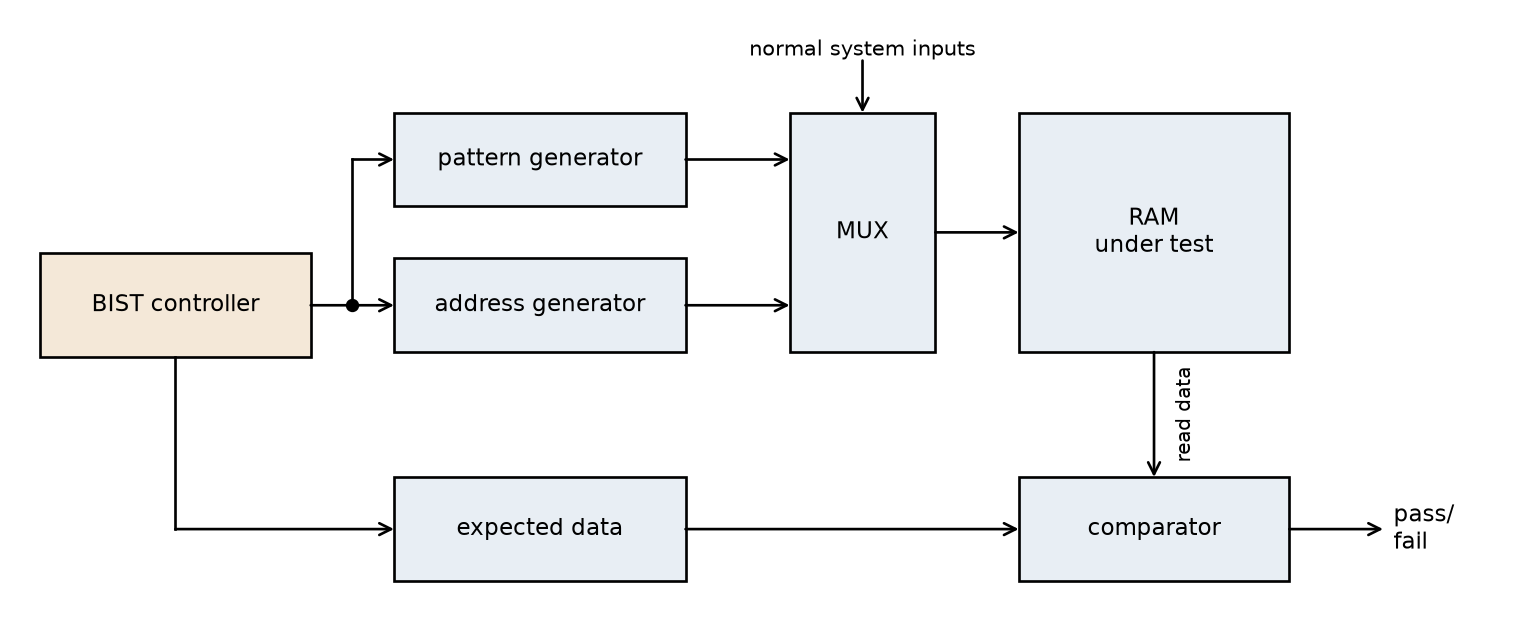
6.5.4 JTAG Test and Debug Port
JTAG (IEEE Standard 1149.1) is a standardized test and debug port using serial communication to access IC-internal functional blocks (like the RAM BIST). JTAG uses four or five additional signals: TDI (test data in), TDO (test data out), TCK (test clock), TMS (test mode select), and optionally TRST (test reset). A two-pin version (cJTAG, IEEE 1149.7) uses only TMSC (test serial data) and TCKC (test clock).
JTAG was originally introduced to check interconnection faults on the PCB level, as solder joints are the main cause of failing boards: all IC pins can be forced to 0 or 1 (or read) via the boundary-scan chain, so all intended PCB connections between ICs can be tested after board manufacturing (see Figure 64). Meanwhile, JTAG is also extensively used to access internal components of an IC for debugging and test.
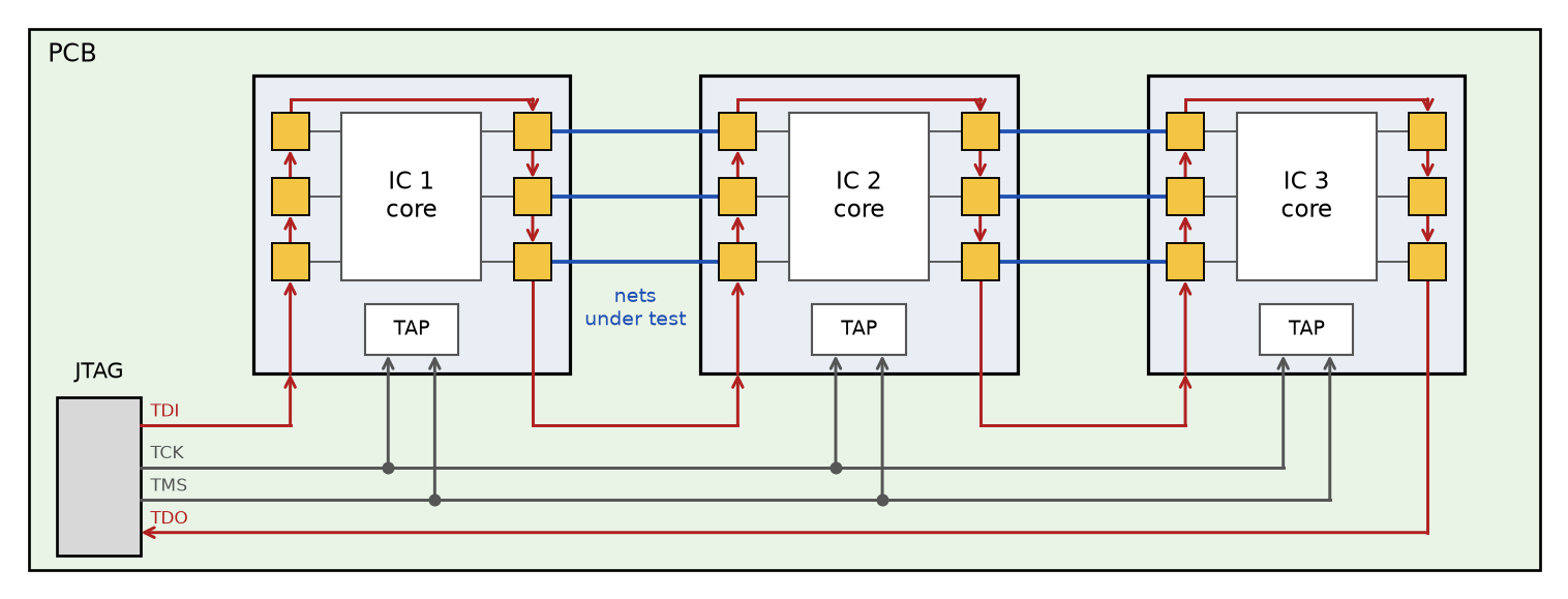
6.5.5 Trimming
If a property of the DUT needs to be trimmed (e.g., a reference voltage, an \(RC\) product, or an SRAM repair map), this property is measured on the tester. This might require a special test mode, where an internal signal is multiplexed to one of the pins, or an internal calibration circuit is triggered and the result is read out digitally. The resulting trimming information is permanently stored inside the DUT:
- If EEPROM bits are available, these can be used.
- Fuses (e.g., polysilicon or metal wires or minimum-size vias melted open) or anti-fuses (e.g., diodes melted into a short) can permanently store a bit by forcing a high current during programming.
- For analog precision circuits, laser trimming on the wafer can be used, e.g., to adjust the value of an integrated resistor.
6.5.6 Scan-Path Test
Digital circuits consist (besides RAM and ROM) of combinational logic and state machines. For testing, two properties of a circuit node matter:
- Observability: the ease of observing a node by watching the external output pins of the IC.
- Controllability: the ease of forcing a node to 0 or 1 by driving the input pins of the IC.
Combinational circuits are controllable and observable, so it is relatively easy to determine test patterns. Sequential circuits, however, have states! Finite state machines can be very difficult to test, requiring many cycles to enter a desired state. Beyond a certain size, exhaustive testing with all possible input vectors becomes impractical: for a circuit with \(N\) inputs and \(M\) state bits, \(2^{N+M}\) patterns would be needed. For example, \(N = 40\) inputs and 32 states (\(M = 5\)) at 10 ns per pattern results in roughly 100 hours of test time.
Chip failures (opens, weak or strong shorts to other nodes) can cause very complex failure behavior, which is too time-consuming to test exhaustively—so a simplified stuck-at model is used: all failures are assumed to make nodes stuck at 0 (shorted to \(V_\mathrm{SS}\)) or stuck at 1 (shorted to \(V_\mathrm{DD}\)). This simple model is not quite true in reality, but works well enough in practice. Its limitation is demonstrated in Figure 65: an open in one pull-up branch of a CMOS NAND gate causes a sequential effect (the output keeps its previous value for one input combination), which needs two test vectors in the right order to be detected.
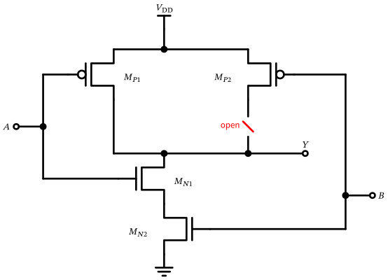
A manufacturing test would ideally check every node in the circuit, applying the smallest sequence of test vectors necessary to prove that each node is not stuck. To increase observability and controllability, i.e., design for test (DFT), the scan-path test is introduced, shown in Figure 66:
- Each flip-flop is converted into a scan register (with a small area overhead): in mission mode, the flip-flops behave as usual; in scan mode, all flip-flops form a shift register, so their contents can be shifted in and out through dedicated pins.
- If each register can be observed and controlled this way, the test problem reduces to testing the combinational logic between the registers.
- During the production test, test patterns are shifted into the scan chains, one clock cycle is applied, and the captured result is shifted out and compared to the expected result (→ pass/fail). Digital pattern generators in the ATE hardware accelerate this.
- The patterns are generated automatically by software (ATPG) from the design netlist, achieving high stuck-at fault coverage with a minimum number of patterns.
- To speed up testing further, multiple chains are operated in parallel (requiring test pins for the parallel chain inputs and outputs).
- An extension of scan is to use internal pattern generators (e.g., based on a pseudo-random number generator) as logic inputs, and to compress the outputs into a syndrome (e.g., a transition count or hash) that is compared to the expected syndrome → logic BIST.
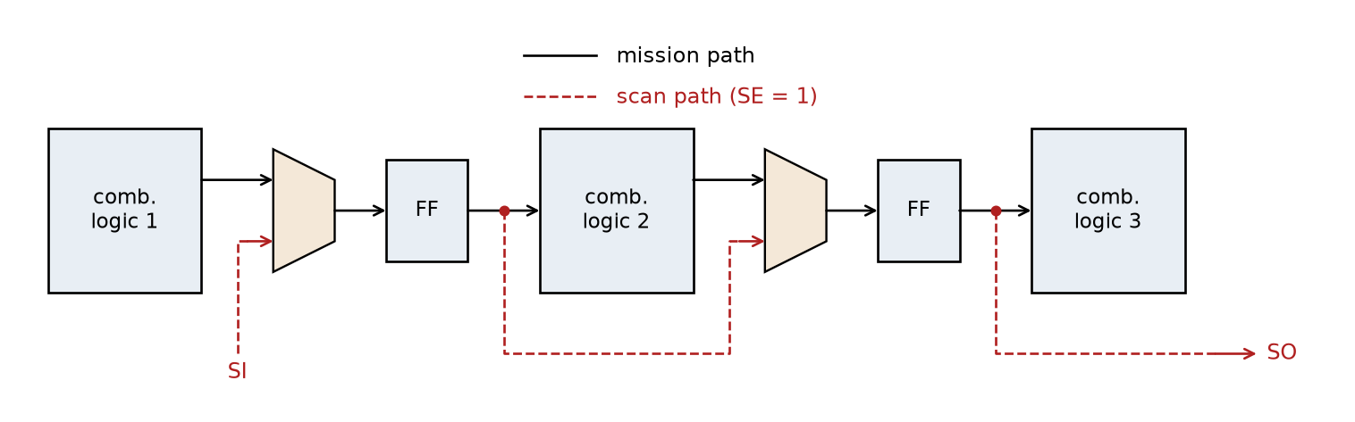
6.5.7 AC Parametric Tests
Analog and mixed-signal parametric tests are highly dependent on the given function; examples are gain, phase, distortion, rejection (CMRR, PSRR), and noise. The DIB must be designed to reflect the conditions of the IC datasheet, e.g., applying the proper output loading (\(R\) and \(C\)); different loads for different tests can be switched in via relays. Noise tests can be very time-consuming due to the long averaging needed to detect small signals; additional circuitry on the DIB can help to increase repeatability and speed.
Modern mixed-signal testers use arbitrary waveform generators (AWGs) and digitizers to create and capture analog signals, with DSPs to speed up signal generation and analysis, as shown in Figure 67. Concepts from sampling theory (quantization noise, under/oversampling, aliasing and reconstruction, FFT, windowing, sampling-clock coherence, etc.) apply!
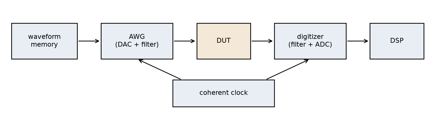
For analog test parameters, the variation over production must stay inside the test limits, which are derived from the datasheet limits minus guard bands: the lower specification limit (LSL) and the upper specification limit (USL).
6.6 Process Capability Index
To manufacture within a specification, the difference between the USL and the LSL must be greater than the total process variation, and the distribution should be well centered between the limits. One way to check this is the \(C_\mathrm{p}\)/\(C_\mathrm{pk}\) analysis (Montgomery 2012). Given a parameter distribution \(x_i\) from a sample of size \(N\), the arithmetic mean and the standard deviation are
\[ \overline{X} = \frac{1}{N} \sum_{i=1}^{N} x_i \qquad \sigma = \sqrt{\frac{1}{N} \sum_{i=1}^{N} \left( x_i - \overline{X} \right)^2} \]
Then, the process capability indices are calculated as
\[ C_\mathrm{p} = \frac{\mathrm{USL} - \mathrm{LSL}}{6 \sigma} \tag{55}\]
\[ C_\mathrm{pk} = \min \left\lbrace \frac{\mathrm{USL} - \overline{X}}{3 \sigma}, \frac{\overline{X} - \mathrm{LSL}}{3 \sigma} \right\rbrace \tag{56}\]
\(C_\mathrm{p}\) measures whether the process spread fits between the limits at all, while \(C_\mathrm{pk}\) additionally accounts for the centering of the distribution. Ideally, \(C_\mathrm{p} = C_\mathrm{pk}\) (the process is well centered), and \(C_\mathrm{pk} > 2\) (which might not be achievable, so lower values like \(C_\mathrm{pk} > 1.5\) may have to be accepted). Figure 68 illustrates well-centered and off-center distributions.
During product qualification, the \(C_\mathrm{p}\)/\(C_\mathrm{pk}\) values are evaluated on a sufficient sample size, and critical tests are improved (change of datasheet limits, better centering of a parameter by redesign, process centering, etc.).
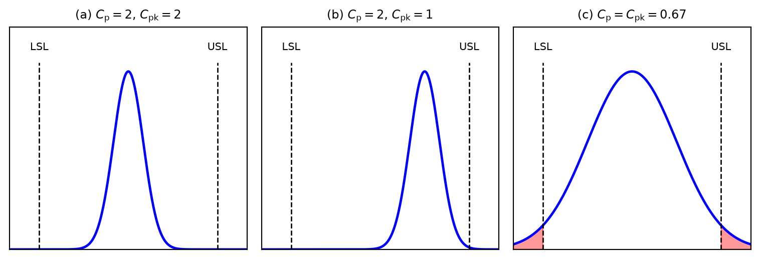
The advantage of using the \(C_\mathrm{p}\)/\(C_\mathrm{pk}\) analysis is that it provides a quantitative measure of both the process spread and the centering of the distribution relative to the specification limits. This helps in automatically identifying whether the process is capable of consistently producing parts within the desired specifications and whether any adjustments are needed to improve yield and quality with just two numbers: \(C_\mathrm{p}\) and \(C_\mathrm{pk}\). Manual inspection of the distribution alone may not reveal subtle misalignments or variations that could impact production quality and can be extremely time consuming and error prone.
7 Economy of Integrated Circuits
The manufacturing of ICs is a large-scale business, requiring significant investment in research and development, and usually large volumes are built and sold. It is therefore rewarding to take a look at the economics of integrated circuits.
7.1 Selling Price and Total Cost
The selling price \(S_\mathrm{tot}\) of a good depends on the achievable profit margin \(m\) and the total cost of the product \(C_\mathrm{tot}\):
\[ S_\mathrm{tot} = \frac{C_\mathrm{tot}}{1 - m} \tag{57}\]
| Profit margin | Selling price |
|---|---|
| 30 % | \(S_\mathrm{tot} \approx 1.4 \cdot C_\mathrm{tot}\) |
| 50 % | \(S_\mathrm{tot} = 2 \cdot C_\mathrm{tot}\) |
| 70 % | \(S_\mathrm{tot} \approx 3.3 \cdot C_\mathrm{tot}\) |
The total cost \(C_\mathrm{tot}\) of a product consists of the non-recurring engineering cost (NRE) \(F'_\mathrm{tot}\) plus other fixed costs \(F''_\mathrm{tot}\) (together \(F_\mathrm{tot} = F'_\mathrm{tot} + F''_\mathrm{tot}\)), and the recurring cost \(R_\mathrm{tot}\). The recurring cost is incurred per IC, whereas NRE and fixed costs relate to the whole project; their impact on the cost per piece thus depends on the number of pieces sold, \(N_\mathrm{sold}\):
\[ C_\mathrm{tot} = R_\mathrm{tot} + \frac{F_\mathrm{tot}}{N_\mathrm{sold}} \tag{58}\]
7.2 Non-Recurring Engineering Cost
The NRE consists of the engineering cost \(E_\mathrm{tot}\), the prototype cost \(P_\mathrm{tot}\), and the cost of licensed IP blocks \(I_\mathrm{tot}\):
\[ F'_\mathrm{tot} = E_\mathrm{tot} + P_\mathrm{tot} + I_\mathrm{tot} \tag{59}\]
Engineering cost: \(E_\mathrm{tot}\) depends on the size of the design team (architecture, design, simulation, layout, timing, DRC & tapeout, test). It includes salaries, benefits, training, computers, and CAD tool licenses. License costs can be substantial in IC design; approximate yearly costs per seat are $10k/yr for a digital front-end seat, $1M/yr for a digital back-end seat, and $100k/yr for an analog front-/back-end seat.
Prototype cost: The mask cost depends heavily on the process technology and the used technology options (e.g., additional \(V_\mathrm{th}\) flavors, analog options like precision resistors or MIM capacitors), which drive up the number of masking steps; see Table 12. A multi-project wafer (MPW), where multiple designs share a single reticle and thus the share also the mask cost, is a good alternative for prototypes. Also test fixtures (sockets, PCBs) and package tooling belong to \(P_\mathrm{tot}\).
| Technology | Estimated mask-set cost |
|---|---|
| CMOS 180 nm | $80k |
| CMOS 28 nm | $1.5M |
| CMOS 5 nm | > $10M |
IP cost: Large SoCs might require licensing of certain IP blocks (interfaces, processor cores, memory, etc.); patent licensing might be required as well. Types of licensed IP are:
- Hard IP: circuit blocks defined at the mask (layout) and transistor (netlist) level.
- Firm IP: logic-level/register netlist.
- Soft IP: described at the register-transfer level (RTL) in an HDL.
Licensed cores must come with documentation, BIST, a test-pattern delivery method, or external test patterns.
Other fixed costs \(F''_\mathrm{tot}\) include datasheets and application notes, marketing and advertising, and yield analysis and production support.
7.3 Recurring Cost
The recurring cost consists of the fabrication cost per IC, considering the wafer manufacturing, packaging, and test:
\[ R_\mathrm{tot} = R_\mathrm{die} + R_\mathrm{pack} + R_\mathrm{test} \tag{60}\]
The packaging cost \(R_\mathrm{pack}\) depends mainly on the type of package and the packaging yield. The test cost \(R_\mathrm{test}\) depends strongly on the type of tester (digital, mixed-signal, RF) and the test time (the duration of the test program including robotic handling); an effective way to reduce test cost is to test several devices in parallel.
7.3.1 Dice per Wafer
The cost per die depends strongly on the cost per wafer \(W\) (on the order of $500 to $30,000), the die area \(A\), the usable wafer diameter \(d\) (nominal wafer diameter minus twice the edge exclusion), and the yield \(Y\):
\[ R_\mathrm{die} = \frac{W}{N \cdot Y} \tag{61}\]
The edge exclusion (EE) is the ring around the circumference where no functional IC can be placed, typically 2 to 3 mm (we use 2 mm here). The number of dice per wafer can be approximated by (\(A\) in mm², \(d\) in mm) (Vries 2005)
\[ N \approx d \pi \left( \frac{d}{4 A} - \frac{1}{\sqrt{2 A}} \right) \tag{62}\]
which is plotted in Figure 69 for the standard wafer sizes.
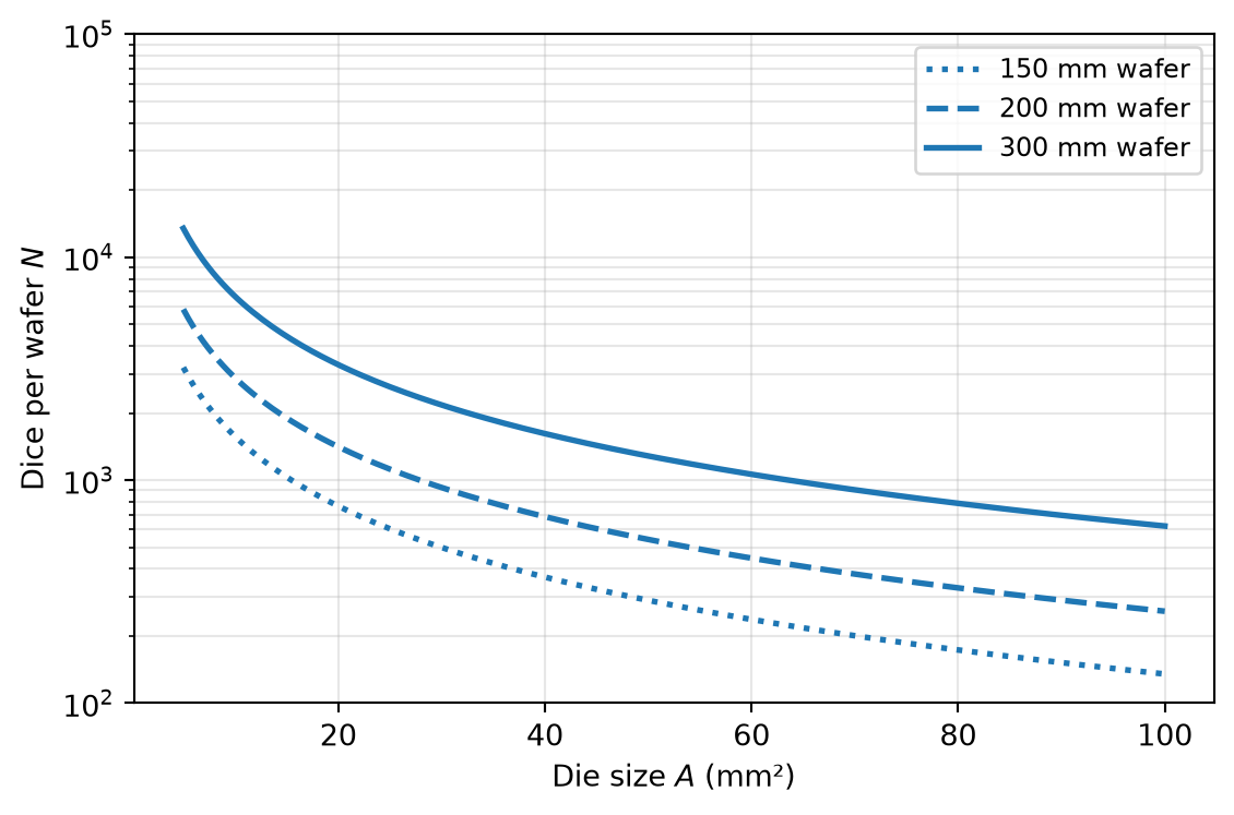
7.3.2 Yield
The yield \(Y\) is the number of functional dice divided by the total number of dice per wafer (\(Y = 50\,\%\) means that half of the produced ICs are defective). Wafer processing incurs a defect density per unit area (\(D_0 \approx 0.01\) to \(1\,\text{cm}^{-2}\)) in the silicon structures—this is why clean rooms and careful processing are essential. The defect density and the die area are related to the yield by Murphy’s model (Murphy 1964):
\[ Y = \left( \frac{1 - e^{- A D_0}}{A D_0} \right)^2 \approx e^{-A D_0} \tag{63}\]
Equation 63 shows that the die size is also a critical factor for yield! Combining Equation 62 and Equation 63 yields the number of good dice per wafer, depicted in Figure 70.
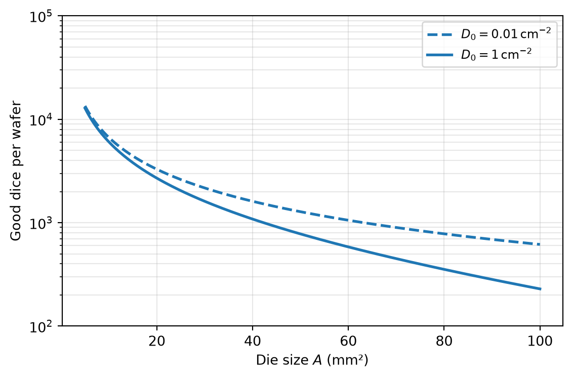
7.4 An Exemplary Calculation
Note 5: IC Cost and Selling Price
Let us calculate the required selling price for an IC using the following assumptions:
| Parameter | Value |
|---|---|
| Wafer cost \(W\) for a \(d = 200\,\text{mm}\) wafer | $1500 |
| Die size \(A\) | 15 mm² |
| Yield \(Y\) | 95 % |
| Targeted gross margin \(m\) | 50 % |
| NRE plus fixed cost \(F_\mathrm{tot}\) | $5M |
| Package and test cost | $0.75 |
Using Equation 62 with \(d = 196\,\text{mm}\) (2 mm edge exclusion), we get \(N \approx 1900\) dice per wafer, and with Equation 61, the cost per die is
\[ R_\mathrm{die} = \frac{\$1500}{1900 \cdot 0.95} = \$0.83 \]
The total recurring cost per die is (using Equation 60)
\[ R_\mathrm{tot} = \$0.83 + \$0.75 = \$1.58 \]
The required selling price is strongly dependent on the number of ICs sold (using Equation 57 and Equation 58):
\[ S_\mathrm{tot} = \frac{1}{1 - m} \left( R_\mathrm{tot} + \frac{F_\mathrm{tot}}{N_\mathrm{sold}} \right) = 2 \left( \$1.58 + \frac{\$5\,\text{M}}{N_\mathrm{sold}} \right) \]
The resulting selling price versus sales volume is plotted in Figure 71: in the left region (low volume), the fixed cost \(F_\mathrm{tot}\) dominates the selling price, whereas for larger volumes the recurring cost \(R_\mathrm{tot}\) becomes crucial.
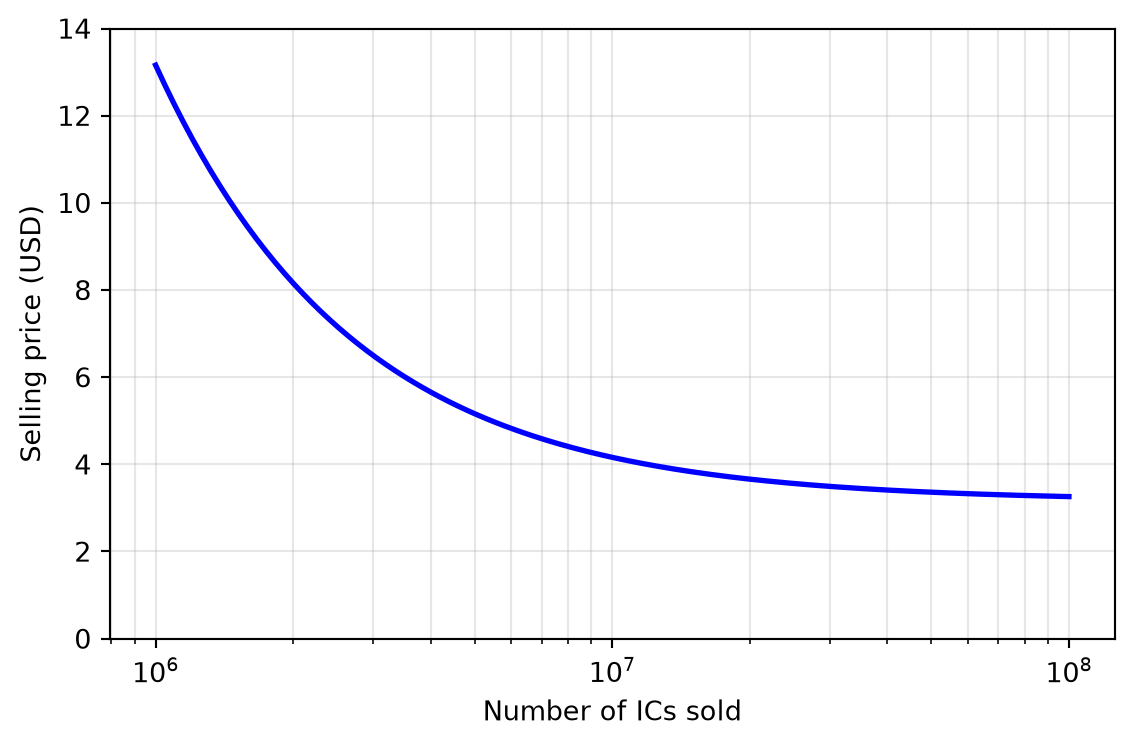
In the example of Note 5, we can clearly see that at low sales volumes, the fixed costs dominate the selling price, whereas at high sales volumes, the selling price approaches twice the recurring cost. Since a fixed-cost dominated IC product is often simply too expensive, it is crucial to achieve sufficient sales volume to make the product economically viable.
8 Design Methodology
In this chapter, basic knowledge of digital and analog circuit design is assumed; we discuss IC-specific design methodology topics which are usually not covered in entry-level courses. A comprehensive treatment of digital VLSI design and its methodology is given in (Weste and Harris 2011). We first introduce a mental model of the design space (the Y-diagram), then survey the available implementation styles and their trade-offs, and finally walk through the concrete design flows—the digital semicustom flow and the analog/mixed-signal custom flow—illustrated throughout with open-source EDA tools.
8.1 The Y-Diagram
A useful mental model for IC design is the Y-diagram (Gajski and Kuhn 1983), shown in Figure 72. A design can be described in three domains—behavioral (what the circuit does), structural (which components it is composed of), and physical (how it is arranged geometrically)—each represented by one axis of the “Y”. Orthogonal to the domains are several levels of abstraction, drawn as concentric rings: from the system level on the outer rings, through the register-transfer and logic levels, down to the transistor (circuit) level in the center. Any design representation is thus a point on one of the three axes at a given abstraction ring. A design step is a transformation between these representations, typically moving from one domain to another and towards lower abstraction (inner rings): for example, logic synthesis transforms a behavioral description (RTL) into a structural one (gate-level netlist), and place-and-route transforms the structural netlist into physical layout. Synthesis steps move inward (refining detail), while abstraction or extraction steps move outward.
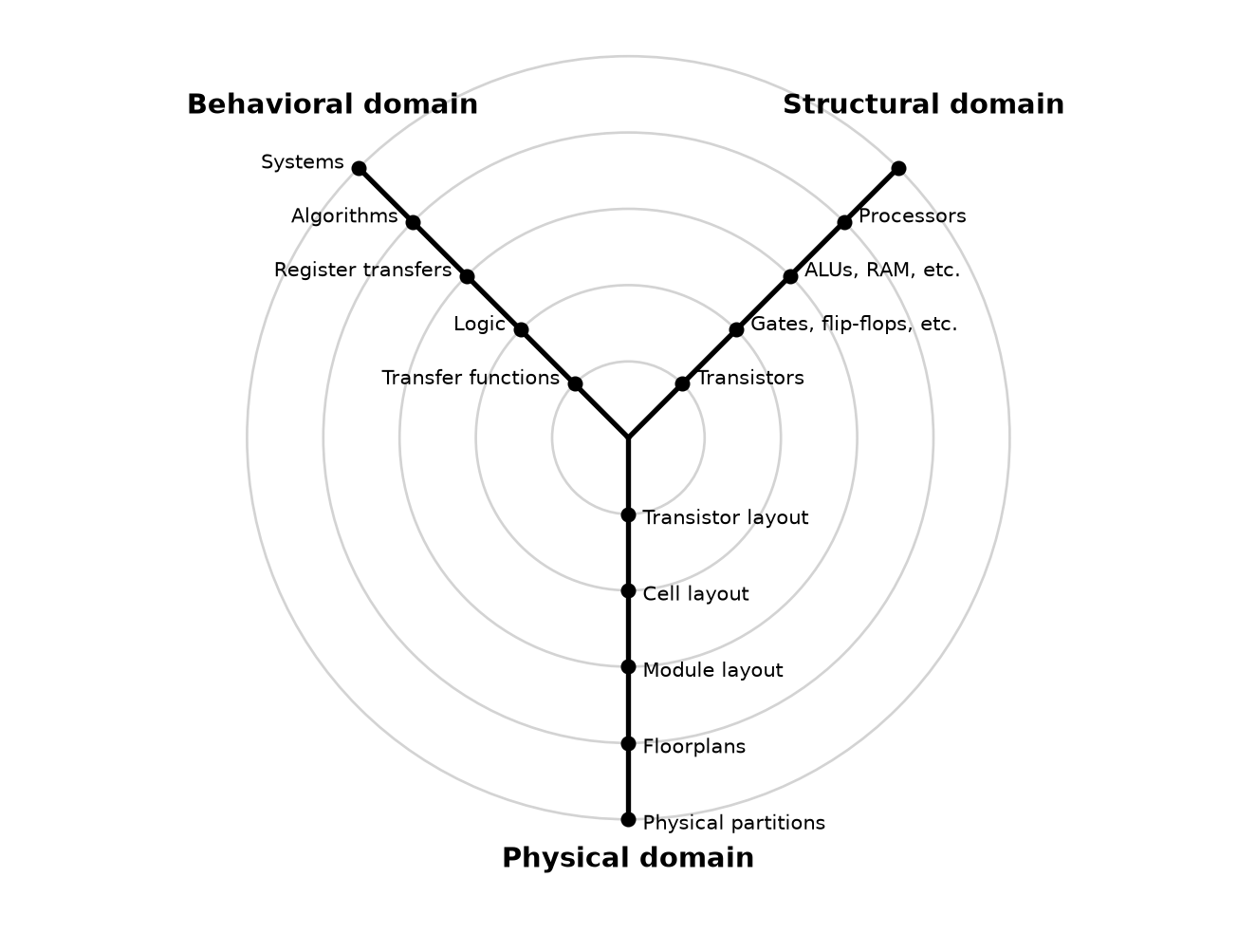
8.2 Digital Implementation Choices
Figure 73 shows the taxonomy of digital circuit implementation approaches, from fully custom design to semicustom cell-based and array-based styles.
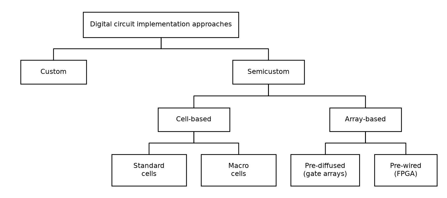
In a fully custom design, every transistor and wire is crafted by hand to maximize performance, density, or both; this is worthwhile for analog blocks, high-speed interfaces, or memory bit-cells that are replicated millions of times, but it is slow and labor-intensive. Semicustom design instead assembles the circuit from pre-designed and pre-characterized building blocks, trading some area and speed for much shorter design time and lower risk. Semicustom styles fall into two groups: cell-based approaches build the design from standard cells and macro cells that are placed and routed (mostly automatically), whereas array-based approaches start from a pre-fabricated array of devices (gate arrays) or programmable logic (FPGAs) and customize only the interconnect.
There usually exists a trade-off between energy efficiency and flexibility:
- Hard-wired logic offers the lowest power consumption, but very little flexibility.
- Software running on a general-purpose CPU is fully flexible, but not power-efficient.
- Software running on a domain-specific processor like a DSP or GPU sits in between.
| Design style | Energy efficiency | Flexibility |
|---|---|---|
| Hardwired custom logic | high | low |
| FPGA | low | high |
| Domain-specific processor (e.g., DSP, GPU) | low/mid | mid |
| General-purpose processor (CPU) | low | high |
Given the trade-offs in Table 13, the architecture of SoCs often involves a careful balance between energy efficiency and flexibility, selecting appropriate implementation approaches for different parts of the system. Often an optimized mix is chosen: fixed-function blocks can be implemented using hard-wired logic for maximum energy efficiency, while programmable blocks can leverage CPUs, DSPs, or domain-specific processors to maintain flexibility with FW updates.
8.3 Cell-Based Design
Different types of cells can be used when designing ICs:
- A high-level description (e.g., in VHDL or SystemVerilog) can be synthesized and automatically placed and routed using standard logic cells.
- Hard macro modules (like SRAM or IO cells) can be used to construct larger designs.
- Soft macro modules (provided as a synthesizable high-level description or RTL) can be integrated as well.
8.3.1 Standard Cell Library
Standard-cell libraries (SCLs) are offered by IP vendors or foundries; a detailed treatment of standard cells and semicustom design is given in (Smith 1997). The following cell types are usually available:
- Logic functions (AND, OR, NAND, NOR, INV, XOR, XNOR) with 2 and more inputs (usually up to 4).
- Complex gates (like combined AND-OR gates, half-adders, bit-shifter cells).
- Auxiliary cells (buffers to balance delays, tie cells to bias n-wells and substrate, decoupling cells, spacers, tri-state buffers, antenna diodes).
- Storage elements (latches, flip-flops).
The logic cells are available in different drive strengths to balance chip area versus propagation delay versus power consumption (active as well as leakage). The cells are thoroughly characterized for timing, power consumption, capacitive load, and leakage versus PVTL (process, voltage, temperature, load), and the results are stored in look-up tables used by the EDA tools.
As an example, Figure 74 shows the transistor-level schematic of a NAND2 standard cell; in the IHP SG13 open PDK, this cell is available in two drive strengths (nand2_1 and nand2_2). Also, various latches and flip-flops are provided, with and without scan-chain support, with optional set and reset, and in different drive strengths (e.g., the scan flip-flop sdfbbp_1 with inverted asynchronous set and reset).
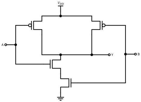
Figure 75 shows the typical layout organization of a standard cell: all the cells have a common height, power is distributed on horizontal \(V_\mathrm{DD}\)/\(V_\mathrm{SS}\) rails at the top and bottom (abutting with the neighbors), the n-well spans the upper half (PMOS devices), and the signal terminals are placed on a routing grid. The height of the cells is fixed to ensure uniformity and ease of placement in rows and is usually given in terms of track height (i.e., the number of routing tracks that fit within the cell height). The width of the cells can vary depending on the complexity and drive strength of the cell, but is based on a grid structure to facilitate routing and alignment with neighboring cells.
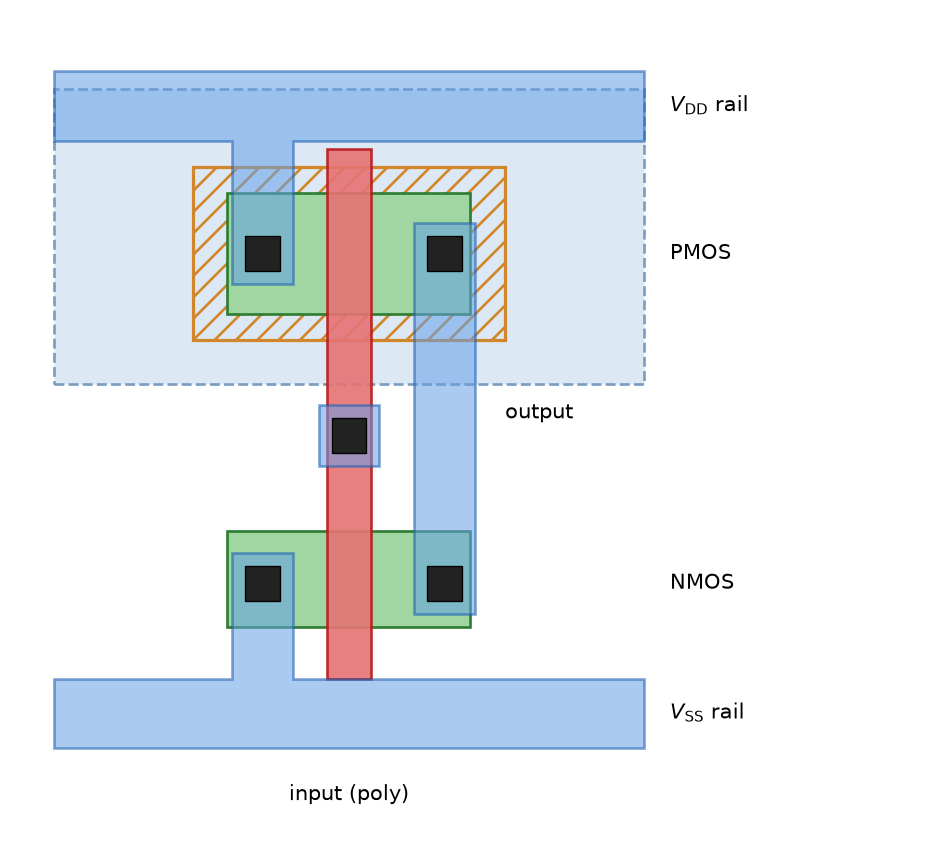
M1 at top and bottom, the n-well with the PMOS in the upper half, the NMOS in the lower half, a shared vertical poly gate as input, and the output on M1.
8.3.2 Hard Macros
Usually read-only memories (ROM), random-access memories (RAM), and one-time programmable (OTP) memories like e-fuses are available as hard macros, created by module generators (“memory compilers”). SRAM generators often provide plenty of options, like the number of rows and columns, with or without repair, built-in self-test (BIST), single- or dual-port, and high-performance or low-leakage variants.
IO cells (input/output cells for interfacing with the external pins of the chip, providing the necessary voltage level shifting, drive strength, and protection circuitry) are often provided as hard macros as well, for example the sg13g2_io library in the IHP SG13G2 open PDK. From these IO cells the padring is constructed, which surrounds the core logic and provides the interface to the external pins.
8.4 The Semicustom Design Flow
Figure 76 shows the semicustom design flow at a high level: the design is captured in an HDL, synthesized to a gate-level netlist, and physically implemented by floorplanning, placement, and routing (RTL2GDS). Simulation accompanies every step (pre-layout simulation of the HDL and the netlist, post-layout simulation with extracted parasitics), and design iterations loop back to earlier stages when timing, power, or functionality goals are not met. The flow is conventionally divided into a front-end part, which turns the behavioral description into a verified gate-level netlist, and a back-end part, which turns that netlist into manufacturable layout; both are detailed in the following subsections. Because a decision made late in the flow—such as a routing detour that adds delay—can invalidate an assumption made earlier, reaching design closure, where timing, power, area, and signal-integrity constraints are met simultaneously, usually takes several of these iterations.
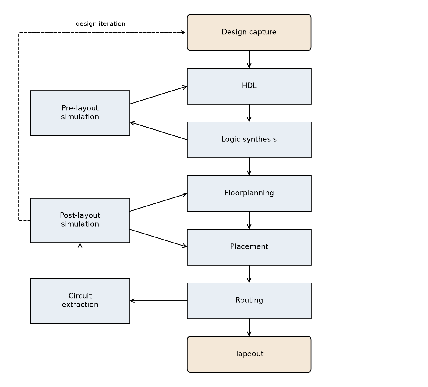
8.4.1 RTL Synthesis
The front-end part of the flow transforms the behavioral description into a verified gate-level netlist, as shown in Figure 77. The behavioral description (VHDL, SystemVerilog) is first verified by simulation; after RTL synthesis and library mapping, the resulting netlist is verified again (by simulation or formal equivalence checking), followed by static timing analysis. Test logic (scan chains, see Section 6.5) is inserted, and the netlist is checked once more, together with a power analysis, before it is handed to physical synthesis. The algorithms behind logic synthesis and optimization are covered in depth in (Micheli 1994). In the open-source flow, the corresponding tools are iverilog or verilator (simulation), yosys (synthesis), abc (logic optimization and mapping), opensta (timing and power analysis), fault (test insertion), and gtkwave (waveform viewing).
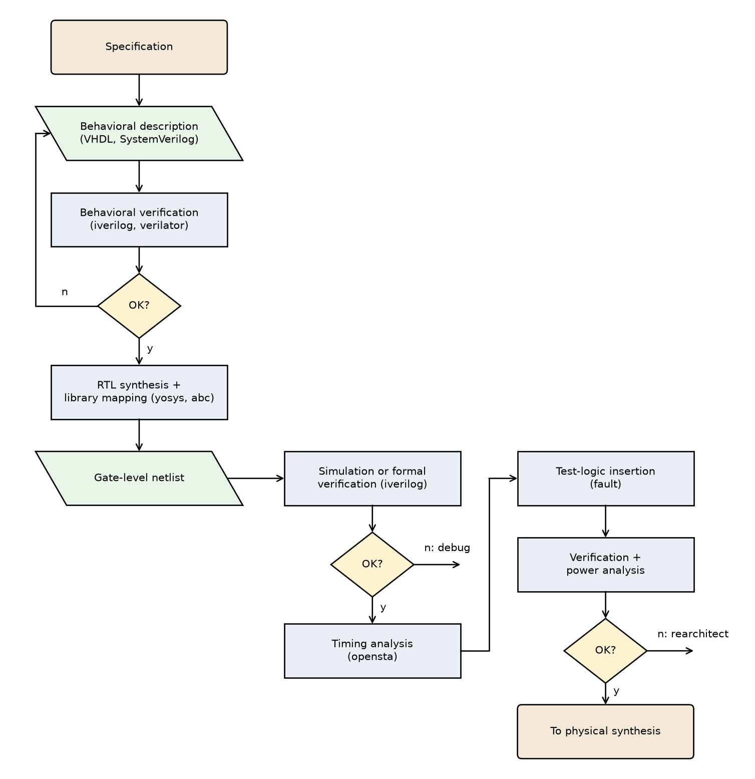
8.4.2 Standard-Cell Place and Route
The back-end part of the flow, shown in Figure 78, turns the netlist into manufacturable layout: placement and routing (openroad) use the library and technology descriptions (LEF), producing the design in DEF format; parasitic extraction (openrcx) generates a SPEF file used for accurate post-layout timing analysis (opensta); after noise and reliability checks pass, the final layout database is streamed out as GDSII (klayout, magic) and sent to the manufacturer. The algorithms of physical design—partitioning, floorplanning, placement, routing, and timing closure—are treated comprehensively in (Kahng et al. 2022).
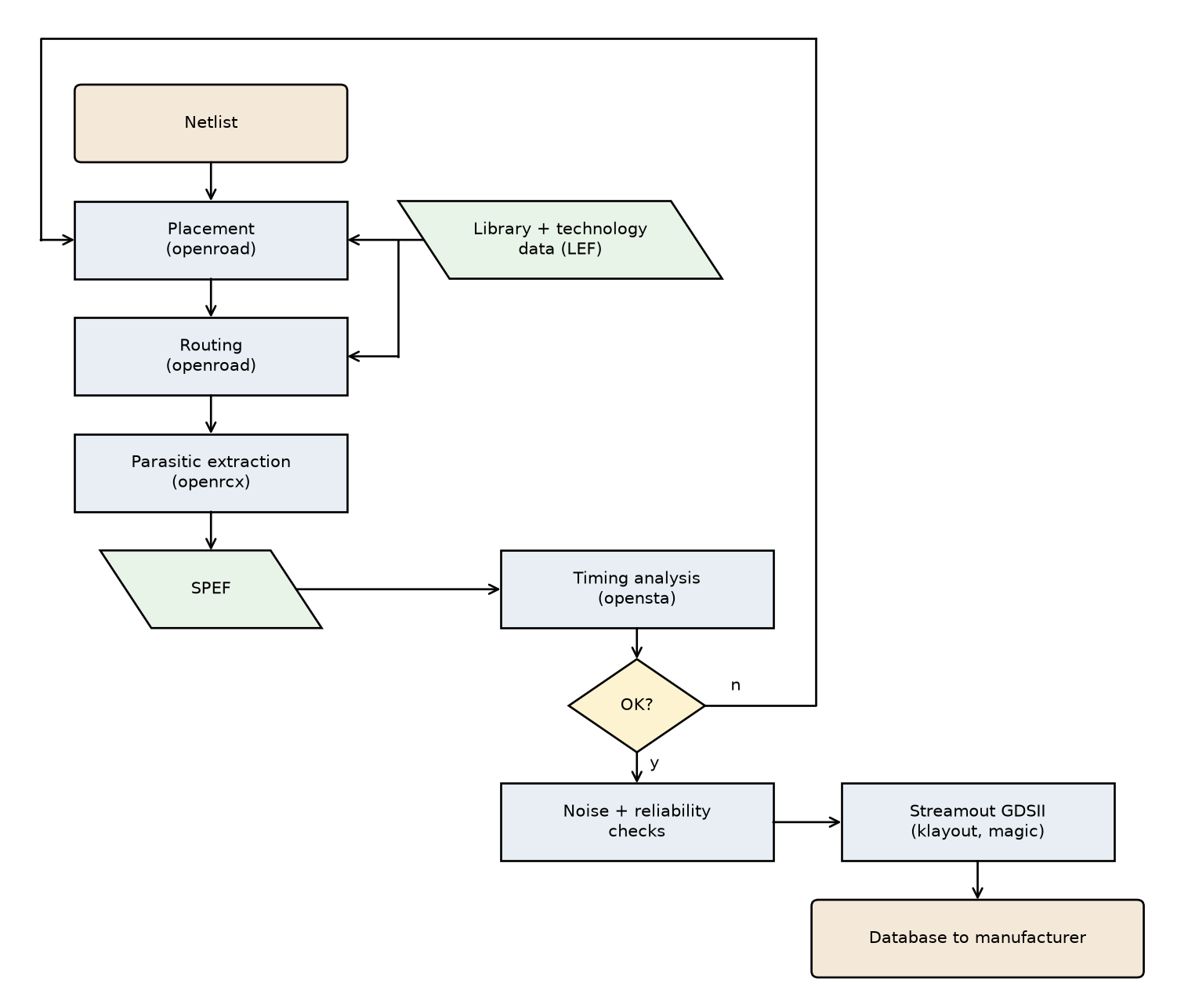
8.4.3 The Open-Source RTL-to-GDS Flow
In recent years, open-source tools have made a huge step forward, so that a complete behavioral (SystemVerilog) to GDSII flow is freely available with OpenROAD and the integrated LibreLane flow. Together with the IHP SG13 open-source PDK—including its open standard-cell library (sg13g2_stdcell)—everything needed for a digital tapeout is now openly available. This has dramatically lowered the barrier to entry for chip design: students, researchers, and hobbyists can take a design all the way from RTL to a manufacturable layout without any commercial tool licenses, and low-cost multi-project wafer shuttle runs make it feasible to obtain real silicon.
8.5 The Mixed-Signal/Custom Flow
For analog and mixed-signal designs, the flow is usually schematic-driven, as shown in Figure 79: the design is captured as a schematic (xschem) or netlist, checked by electrical rule checks, and simulated (ngspice, vacask). The layout is constructed manually (klayout, magic), verified by DRC (klayout or magic), and compared against the schematic (LVS with klayout or netgen). After LVS passes, parasitic extraction (magic or klayout-pex) delivers a netlist with layout parasitics, which is back-annotated into the schematic and re-simulated; after reliability checks, the block or IC is ready.
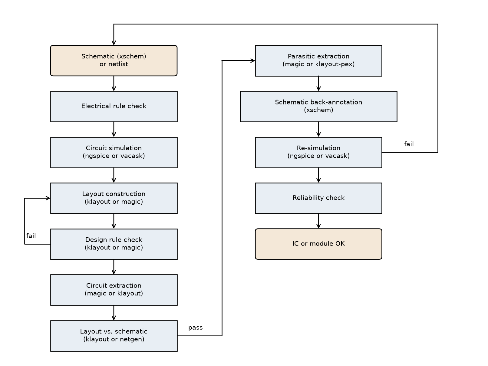
8.6 FPGAs
Field-programmable gate arrays (FPGAs) are a good alternative to a custom digital IC, because the initial cost is very low, and the same HDL description can be used to program an FPGA or to create a semicustom digital design:
- An FPGA consists of programmable logic blocks (typically look-up tables (LUTs) paired with flip-flops), hard macros (like CPUs, DSP slices, memory blocks, or high-speed interfaces), and a programmable interconnect fabric.
- The flexibility is very high (the FPGA can be loaded with a new bit-stream at any time), and the performance can be high as well; however, power consumption and unit cost can be substantial.
- FPGAs can also be used as (more or less) real-time test vehicles for HDL code (for prototyping and software development) before committing to a costly mask set.
The choice between an FPGA and a custom IC is largely a question of volume: FPGAs win at low to medium volumes, where their high per-unit cost is outweighed by the avoided NRE (mask set and design effort) of a custom IC, while an ASIC becomes cheaper per piece once the volume is large enough to amortize its NRE. Many products therefore start on an FPGA and are migrated to an ASIC only once the volume and specification have stabilized.
9 Electrostatic Discharge and Latch-Up
This chapter covers two reliability hazards that every IC design must handle: electrostatic discharge (ESD), the sudden discharge of statically charged objects into the chip, and latch-up, the unwanted triggering of parasitic bipolar structures in CMOS. The treatment of ESD follows (Amerasekera and Duvvury 2002); overviews of ESD test methods and of protection structures can be found in (Ker et al. 2001; Ker and Chuang 2002).
9.1 Electrostatic Discharge
When an external object at a high potential (e.g., charged by the triboelectric effect or by induction from an electric field) touches one of the connections of a circuit, the resulting electrostatic discharge produces a large transient voltage or current—for example, when ICs are handled by humans or by machines with faulty grounding. ESD can even occur without actual contact, as an arc across an air gap. Devices sustain two types of permanent damage as a result of ESD:
- A thin isolation layer (like the gate oxide) may break down, leading to a low-resistance path between structures that should be isolated.
- Diodes, resistors, or wiring may melt while carrying the large discharge current, creating a short or an open.
9.1.1 ESD Models for Testing
Three standardized models are used for ESD testing of ICs, differing in the equivalent charge storage and discharge path:
- The human-body model (HBM): a 100 pF capacitor discharged through 1.5 kΩ, modeling the touch of a charged person.
- The charged-device model (CDM): the IC itself is charged and discharges abruptly through a single pin, modeling machine handling.
- The machine model (MM): a 200 pF capacitor discharged with negligible series resistance, modeling charged (metallic) machinery (largely superseded by HBM/CDM testing today).
Each model defines the charging voltage of an equivalent capacitance and the discharge network—this defines the ESD pulse shape and the peak discharge voltage and current. An “HBM level of 1 kV” means the model capacitance is charged to 1 kV before the discharge. The equivalent circuit and the resulting pulse shapes are shown in Figure 80 and Figure 81: the HBM produces a comparatively long pulse (~150 ns decay) causing mostly thermal stress, while the CDM produces a very short (~1 ns) pulse with high current, leading to large on-chip voltage drops.
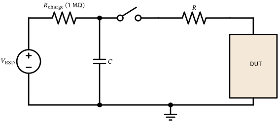
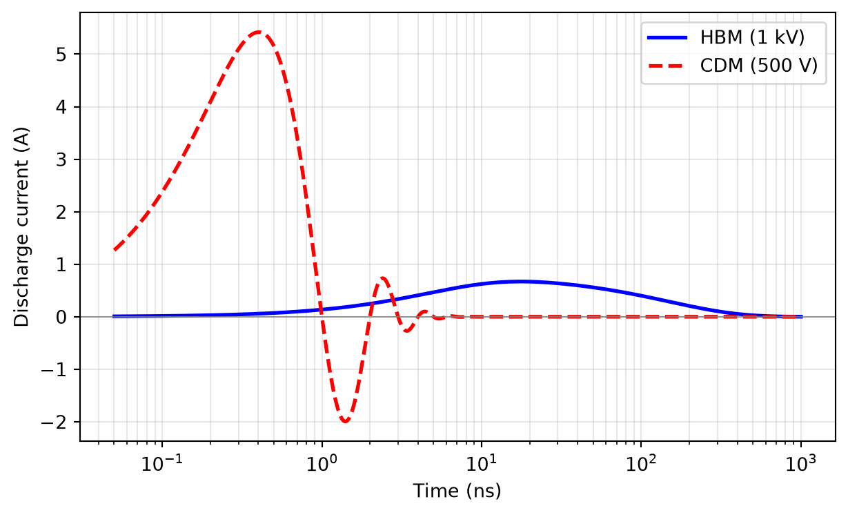
In a CDM event, the charge stored in the body of the IC is discharged when some pin touches external ground; discharge currents of several amperes with rise times below a nanosecond are typical. HBM testing is standardized in ANSI/ESDA/JEDEC JS-001, CDM testing in JS-002.
9.1.2 ESD Protection Concept
All inputs and outputs of an IC (including \(V_\mathrm{DD}\) and \(V_\mathrm{SS}\)) have to be protected against ESD. The protection circuits are usually bundled in a pad library providing optimized I/O cells (digital input/output, analog input/output, RF input/output, supply pads). The protection elements are made from the devices available in the technology, optimized for high-current/high-voltage operation—usually they are provided and qualified by the wafer foundry.
Figure 82 shows the general protection scheme of a (bidirectional) digital I/O:
- The primary ESD element (typically a pair of large diodes to the rails, like \(D_{1,2}\), or a snapback device) provides the main low-ohmic path for a positive or negative ESD pulse.
- The series resistor \(R_\mathrm{in}\) (typically around 500 Ω) limits the current into the secondary protection, which clamps the voltage at the gate oxide of the input receiver.
- The secondary protection (typically a gate-protected NMOS or a diode to the rails, like the shown \(D_{3,4}\)) clamps the voltage at the input of the receiver, protecting the gate oxide from ESD stress.
- The power clamp between \(V_\mathrm{DD}\) and \(V_\mathrm{SS}\) provides a discharge path between the rails, preventing an ESD-induced rise of the supply voltage from damaging core circuits.
- All diodes and clamps are reverse-biased (off) during normal operation. A positive ESD pulse at the pad is discharged via the upper diode and the power clamp to ground; a negative pulse is discharged via the lower diode.
- The receiver might implement additional functionality for the digital input, like Schmitt-trigger action or input filtering.
- The driver consists of large output devices (NMOS and PMOS) that provide the necessary drive strength for the digital output, while the series resistance and protection elements safeguard the driver during ESD events. Additional features might be a tri-state capability or slew-rate control. A (small) series resistance \(R_\mathrm{s}\) in the drain path helps divert the ESD current into the protection devices, at the cost of degrading the driver in normal operation. Often, this series resistance is implemented by extending the drain region of the MOSFETs and blocking the silicide (recall the
OPlayer from Section 4.2), similar to the technique used for the RC-triggered power clamp. - The layout of the protection elements is critical: they should be placed close to the pad to minimize parasitic inductance and resistance, ensuring a fast response to ESD events.
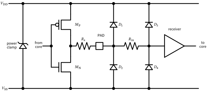
9.1.3 Analog and RF Pads
\(V_\mathrm{DD}\) pads and digital input-only or output-only pads are easily derived from the general I/O pad shown in Figure 82. Analog input and output pads are more critical, since the series resistances (\(R_\mathrm{s}\), \(R_\mathrm{in}\)) might be prohibitive for the intended circuit function; usually, special ESD protection tailored to the specific function is designed for analog pins. For high-frequency pads, ESD protection is highly critical: often no series resistance is acceptable at all, and the protection elements add parasitic capacitance that limits the bandwidth of the I/O. Since the size of an ESD element is determined by the required low resistance and thermal dissipation, RF I/Os often limit the ESD rating of an RFIC, and RF ESD protection is always custom-designed (see, e.g., Ker et al. 2000).
9.1.4 Snapback Devices: The ggNMOS
A popular primary protection element is the grounded-gate NMOS (ggNMOS), shown in Figure 83. In normal operation, the NMOS is off, since its gate is tied to \(V_\mathrm{SS}\). During a positive ESD event, the drain-bulk diode breaks down (reversibly) by avalanche multiplication and injects current into the substrate; this current, together with the substrate resistance \(R_\mathrm{sub}\), forward-biases the source-bulk junction, turning on the parasitic lateral NPN transistor (drain = collector, bulk = base, source = emitter). The device “snaps back” to a low holding voltage and conducts the ESD current between drain and source. A silicide-blocked extended drain improves the robustness by ballasting the current across the device width.
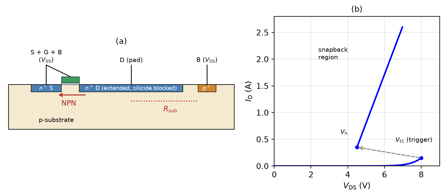
9.1.5 RC-Triggered Power Clamp
Figure 84 shows an RC-triggered supply clamp: during normal operation, the capacitor is charged to \(V_\mathrm{DD}\), the inverter output is low, and the large clamping NMOS \(M_\mathrm{ESD}\) is off. During a (positive) ESD event, the supply rail rises much faster than the RC time constant, the capacitor voltage cannot follow, the inverter input stays low, and its output turns \(M_\mathrm{ESD}\) on—providing a conducting path for the ESD current between the rails.
Beware that a fast \(V_\mathrm{DD}\) ramp during power-up can falsely trigger such a clamp! For this reason, when building the power supplies of electronic systems, designers often include additional circuitry to control the ramp rate or to temporarily disable the RC-triggered clamp during power-up. Considering also the potentially large inrush current \(I_\mathrm{rush} = C_\mathrm{decoup} \cdot dV_\mathrm{DD}/dt\), a controlled supply ramp during supply turn on is essential.
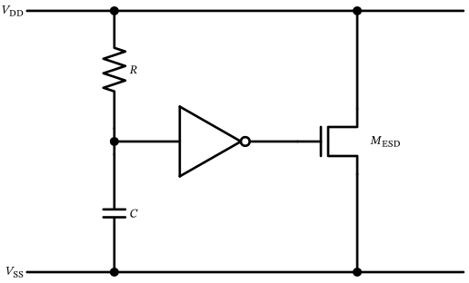
9.1.6 The Silicon-Controlled Rectifier
A silicon-controlled rectifier (SCR, thyristor) can be formed in standard CMOS by utilizing the available diffusions (\(n^+\) and \(p^+\)) and wells (n-well and p-substrate/p-well), forming a PNPN structure, shown in Figure 85. The structure contains two cross-coupled parasitic bipolar transistors (a vertical PNP and a lateral NPN); if the loop gain of the two transistors satisfies
\[ \beta_\mathrm{NPN} \cdot \beta_\mathrm{PNP} \geq 1 \tag{64}\]
then the SCR triggers and provides a very low-ohmic path (snapback). Deliberately built SCRs are excellent ESD protection devices, but the same structure exists parasitically in every CMOS inverter—which brings us to latch-up.
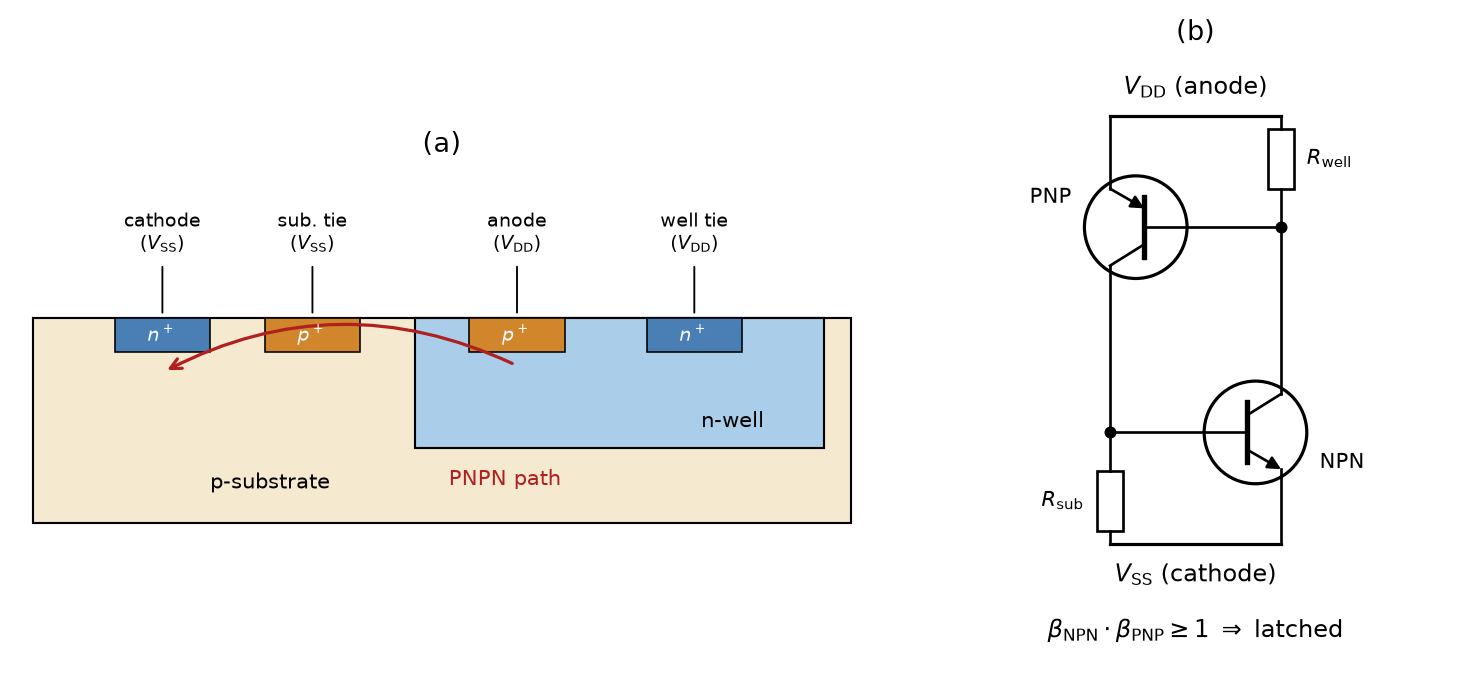
9.1.7 ESD-Protected Areas
On-chip protection is dimensioned for the standardized qualification levels (a few kV HBM, several hundred volts CDM); it does not make a chip immune to the tens of kilovolts that a person or a machine accumulates during handling. Everything outside the chip therefore has to be controlled as well: wafer test, assembly, board manufacturing, and laboratory work are carried out inside an ESD-protected area (EPA), as specified in IEC/EN 61340-5-1 and ANSI/ESD S20.20.
The principle of an EPA is simple: no ungrounded conductor and no charged insulator is allowed near an unprotected device, and all conductive objects—the operator included—are kept at the same potential, so that no discharge can occur in the first place:
- Grounding of all conductors: benches, tools, equipment, chairs, and carts are bonded to a common ground point. The connections are deliberately dissipative rather than metallic (typically \(10^6 \ldots 10^9\,\Omega\)), so that charge bleeds off slowly instead of flowing as a fast, damaging current pulse.
- Personnel grounding: wrist straps (with an integrated 1 MΩ resistor for operator safety) at the bench, plus dissipative shoes and flooring while walking—walking across an insulating floor charges a person to several kV within a few steps.
- Dissipative work surfaces and floors, avoiding both metal (discharge too fast) and plastic (charges up and cannot be discharged).
- Ionizers neutralize the insulators that cannot be grounded at all—plastic housings, PCB base material, documents, clothing—by blowing ionized air across the workplace.
- Humidity control (typically 40 … 60 % relative humidity) raises the surface conductivity of insulators and strongly reduces triboelectric charging; dry air in winter is a classic cause of field failures.
- ESD-safe packaging: devices leave the EPA only inside shielding (Faraday) bags, conductive trays and tubes, or dissipative foam, and are unpacked only inside another EPA.
- Marking, training, and auditing: the EPA boundary is marked, wrist straps and mats are verified regularly (typically per shift), and personnel is trained—an EPA is a process, not just a set of equipment.
ESD-sensitive devices and their packaging carry the ESD susceptibility symbol, whereas the EPA boundary and the protective equipment itself carry the ESD protective symbol, shown in Figure 86.
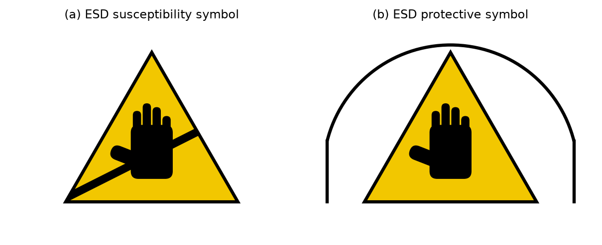
9.2 Latch-Up
Latch-up is the creation of a low-impedance path between the power-supply rails (\(V_\mathrm{DD}\) to \(V_\mathrm{SS}\)) by triggering the parasitic SCR formed by the complementary devices in CMOS, shown in Figure 87 and already discussed in Section 9.1.6. The vertical PNP (emitter = PMOS source in the n-well, base = n-well, collector = substrate) and the lateral NPN (emitter = NMOS source, base = substrate, collector = n-well) form a PNPN structure between the rails, with the well and substrate resistances \(R_\mathrm{well}\) and \(R_\mathrm{sub}\) completing the classic thyristor equivalent circuit.
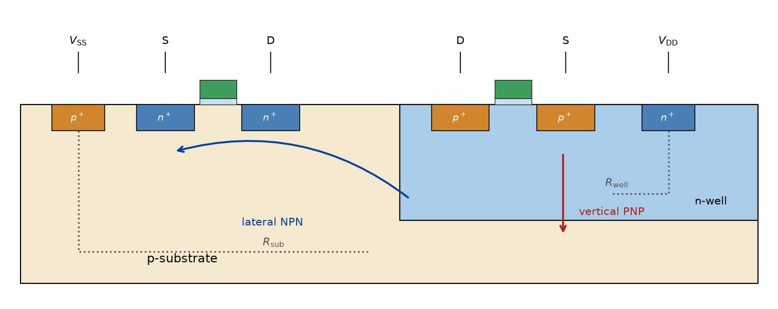
Latch-up is triggered by a current or voltage stimulus on an input, output, or I/O pin (injecting carriers into wells or substrate), or by an over-voltage on the supply pin. Two cases are distinguished:
- Transient latch-up: the low-impedance state persists only while the stimulus is applied.
- True latch-up: the state remains after the stimulus is removed and can only be ended by a power-supply shutdown—use a current limit on the power supply when testing ICs in the lab! The large current can destroy the chip by overheating and electromigration.
9.2.1 Latch-Up Testing
Latch-up testing is a standard procedure during IC qualification (JEDEC JESD78): a current-limited (typically 100 mA), 10 ms pulse is applied to all pads, with the voltage compliance constrained to 1.5× the maximum supply voltage above ground and to a defined negative value below ground; additionally, a supply over-voltage test is applied. After each stimulus, the supply current is monitored to detect a latched state.
9.2.2 Latch-Up Prevention
Latch-up is prevented by weakening the parasitic bipolar transistors and their coupling:
- Physical separation of the diffusions/wells forming the parasitic BJTs lowers their current gain (shallow-trench isolation helps to increase the electrical distance without a large spacing penalty).
- Reduce the parasitic resistances \(R_\mathrm{well}\) and \(R_\mathrm{sub}\) that develop the triggering base-emitter voltages: place many well and substrate ties, and/or use an epi-process with a highly doped substrate.
- Use guard rings around critical components (e.g., I/O drivers and any junction that may inject carriers) to collect stray charges before they can reach a parasitic base, as shown in Figure 88.
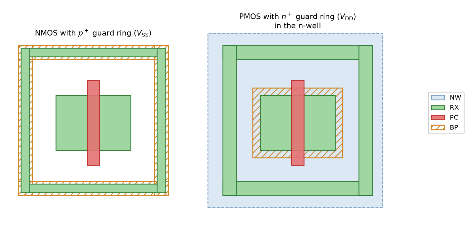
Adopting these design practices helps to significantly reduce the risk of latch-up in CMOS circuits.
Foundries cast these practices into their design rule manuals. IHP SG13G2, for example, dedicates Sec. 7.2 Latch-up Guidelines of the SG13G2 layout rules to the topic:
- For output buffers, the sources of the NMOS and PMOS have to be tied to \(V_\mathrm{SS}\) and \(V_\mathrm{DD}\) and their drains connected directly to the pad; guard rings (well and substrate ties) are required around every device directly tied to a pad, and double guard rings (an n-well isolator plus a \(p^+\) isolator) have to be placed between the n-channel and p-channel buffers, as well as between the buffers and the internal circuitry.
- Rules
LU.aandLU.blimit the maximum distance from any \(p^+\) active area inside the n-well to an n-well tie, and from any \(n^+\) active area inside the p-well to a substrate tie, to 20 µm—this is the rule-deck version of “place many well and substrate ties”. - Rules
LU.ctoLU.d1limit how far a tie may extend beyond its contact (6 µm), which keeps the resistance of the tie itself low.
Beware: these latch-up rules are not checked by default in the SG13G2 DRC deck—the check has to be enabled explicitly.
10 Robust Design
Better than debugging a failing IC is avoiding design issues up front! A good overall strategy for IC design is:
- Go for robust circuits and layouts that are insensitive to PVT (process, voltage, temperature) influences.
- Keep in mind that fabrication variations are normal; use the foundry-supplied corner models to check the design against parameter excursions and component mismatch.
- PCB, IC package, and on-chip wiring all add \(R\), \(L\), \(C\), \(k\) parasitics—model them properly and include them in the circuit simulation.
- During all phases of design and layout, think about what could go wrong, and build in remedies for debug and fix (layout locations where a cut or short can easily be made by FIB or a metal redesign, spare elements, programmability).
This chapter follows these four points, and closes with structured methods and tools for the case where, despite all precautions, first silicon does not behave as expected.
10.1 Robust Circuits and Layouts
Absolute parameters of IC components (MOSFETs, \(R\), \(C\)) vary a lot in production (\(V_\mathrm{th}\) by \(\pm 100\,\text{mV}\), other parameters by ±10 to ±30 %), but ratios can be produced very accurately. Therefore:
- Define gains by resistor ratios or capacitor ratios.
- Set currents by the ratio of a current mirror.
- Time as a parameter can be handled efficiently and accurately (crystal-referenced); if possible, base the circuit principle on timing.
A few further circuit-level habits make a design tolerant against the remaining variations:
- Use negative feedback: the closed-loop gain of an amplifier is set by the feedback network (a ratio again), and is largely independent of the poorly controlled open-loop gain.
- Derive bias currents from a well-defined reference (e.g., a bandgap voltage across a resistor, or a constant-\(g_\mathrm{m}\) bias) instead of a plain supply-referenced resistor, so the circuit performance tracks with process and temperature in a controlled way.
- Prefer differential signal paths: supply noise, substrate coupling, and even-order distortion appear as common-mode disturbances and are rejected to first order.
- Where the achievable accuracy is not sufficient, plan for calibration or trimming (see Section 6.5) instead of over-designing the circuit.
Mismatch of IC components is inherent to wafer production, but can be made worse by bad layout or non-matched sizing: matching is best when devices are constructed from unit elements, with matched size, orientation, wiring, and current-flow direction (see Section 4.5). The random part of the mismatch between two identical, closely spaced devices scales with their area, as described by the Pelgrom model (Pelgrom et al. 1989):
\[ \sigma(\Delta V_\mathrm{th}) = \frac{A_{V_\mathrm{th}}}{\sqrt{W L}} \tag{65}\]
The matching coefficient \(A_{V_\mathrm{th}}\) is supplied by the foundry and is in the range of a few \(\text{mV}\cdot\mu\text{m}\) for current CMOS technologies. With \(A_{V_\mathrm{th}} = 5\,\text{mV}\cdot\mu\text{m}\), a transistor pair with \(W L = 1\,\mu\text{m}^2\) has \(\sigma(\Delta V_\mathrm{th}) = 5\,\text{mV}\); halving the mismatch costs four times the area (and capacitance). Equation 65 is thus a fundamental trade-off between accuracy, area, and speed, which is analyzed in detail in (Kinget 2005); practical layout measures for matching and robustness are collected in (Hastings 2006).
Keep the production flow in mind to anticipate good layout practices: masks can be offset relative to each other, gradients across the wafer will happen, single defects should not cause circuit failure (use multiple vias!), and the layout will be post-processed for manufacturability (filling, cheesing, dummy structures).
Robustness also has a lifetime dimension: a circuit that works at time zero has to keep working over years of operation (see Section 3.10). Relevant wear-out mechanisms are electromigration in wires and vias (respect the current-density limits of the PDK, especially for supply lines and output drivers), gate-oxide breakdown (TDDB), and \(V_\mathrm{th}\) drift by hot-carrier injection (HCI) and bias-temperature instability (NBTI/PBTI). Hence, keep all device terminal voltages within the rated limits of the respective device type in all operating states—including power-up, power-down, and when a block is disabled.
10.2 Corner Models
To check the influence of production parameter variations, the foundries supply corner models. Model files are provided for the nominal corner (TT), reflecting the target values of production, and for the expected parameter extremes (usually \(3\sigma\) to \(5\sigma\)):
- Smallest/largest \(R\), smallest/largest \(C\), etc.
- Slow/fast PMOS and slow/fast NMOS, usually grouped into the corner sets SS, SF, TT, FS, FF (first letter NMOS, second letter PMOS).
All available corner files should be simulated to check the circuit performance against production spread; in addition, temperature and supply voltage (defined early in the IC specification) have to be varied. This results in many simulation runs, requiring automated simulation control and data post-processing. Which combination is the worst case depends on the circuit and on the parameter under test:
- For digital timing, the slow corner (SS, lowest supply, highest temperature) usually limits the maximum clock frequency (setup time), whereas the fast corner (FF, highest supply, lowest temperature) is critical for hold-time violations and leakage. In advanced low-voltage nodes, temperature inversion can make low temperature the slowest condition.
- The skewed corners SF and FS are critical for circuits relying on a balance between NMOS and PMOS, such as the switching threshold of an inverter, ratioed logic, or SRAM cells.
- Analog circuits can have their worst case in any corner, so no corner should be skipped.
Component mismatch (as opposed to global process shift) is covered by Monte-Carlo models, in which device parameters are randomly varied for each simulation run according to their statistical distribution. The result is a distribution of the circuit performance (e.g., the input offset of a comparator), from which mean and standard deviation are estimated. Since a specification is usually required to be met with a margin of several \(\sigma\) (see Section 6.6), and the estimate of \(\sigma\) itself is uncertain for few samples, a meaningful Monte-Carlo analysis needs at least a few hundred runs. Corner models describe the (fully correlated) global process shift, while Monte-Carlo mismatch describes random local variations; for critical blocks, both have to be combined, i.e., Monte-Carlo mismatch runs are performed on top of the process corners.
Note that stacking all worst cases at their extremes (slowest process, lowest supply, highest temperature, \(3\sigma\) mismatch, maximum parasitics) quickly leads to an over-designed circuit wasting power and area. A good specification states which conditions have to be met simultaneously.
10.3 Include the Parasitics
All circuit wiring adds \(R\), \(L\), \(C\), \(k\) parasitics: PCB traces and cables, package parasitics like bond wires, and on-chip interconnect. Having a unified simulation setup capturing all these impairments is a must, as unwanted effects like crosstalk or degraded performance can often be root-caused to them:
- For first investigations, hand-calculated values are a good starting point (see Section 5.5).
- For on-chip circuits, parasitic extraction (PEX) of the layout blocks is mandatory (see Section 4.8).
- For IC packages, first-order lumped models can be refined by calculated EM models (e.g., \(S\)-parameters).
- The same holds for PCB effects; if no simulation model is available, approximate the important effects by calculating \(R\), \(L\), \(C\), \(k\) from the geometry.
Parasitics that are easily overlooked, because they are not part of the signal path, are those of the supply and ground network: a current step through the bond-wire inductance causes supply and ground bounce (\(L\,di/dt\)), and resistive on-chip supply lines cause static and dynamic IR drop. These disturbances couple into every block sharing the same supply, and also into the substrate, which connects all devices on the die through a resistive network (Afzali-Kusha et al. 2006). Common remedies are on-chip decoupling capacitors, separate supply and ground pins for noisy (digital, output drivers) and sensitive (analog, RF) blocks, multiple parallel bond wires, and guard rings around sensitive circuits. When no model of such an effect exists, add a pessimistic estimate to the testbench—an ideal supply and a perfect ground hide exactly the problems that show up in the lab.
10.4 Failure-Mode Thinking
During the complete design phase, an important habit is “failure-mode thinking,” i.e., asking “what could go wrong?” (paranoia is a good trait in IC design). By anticipating potential issues, remedies and debug hooks can be built into the design. Some examples:
- If feedback-loop stability is a concern, make the compensation components (feedback \(R\) and \(C\)) programmable (using register bits and transmission gates to switch components in and out).
- If there is a critical bias point in the circuit, make it observable (connect it to a test pad via a T-gate) or programmable (adapt voltages or currents by programming, metal redesign, or FIB).
- For complex logic functions, add spare logic gates nearby (a few NAND gates, inverters, latches, and delay elements) to allow fixing overlooked logic bugs in a metal-only redesign.
- If circuit sizing is uncertain, place spare elements (\(R\), \(C\), MOSFETs, logic gates) that can be connected in a metal redesign, or by FIB for a handful of repaired samples; often, dummy elements can double in this role.
- If the risk is very high, implement multiple design variants of a circuit on one tape-out, so the best variant (based on measurements) can be selected and refined for the next tape-out.
- Route internal nodes that are hard to measure (bias voltages, reference clocks, the output of a sub-block) to an analog test bus or a test multiplexer, and provide bypass and loop-back modes, so each block of a signal chain can be characterized in isolation.
- Make sure the circuit always reaches its intended operating point: self-biased circuits like bandgap references and current references can have a second, degenerate stable state (all currents zero) and need a start-up circuit. Power-up and power-down sequences, undefined reset states, and floating inputs of disabled blocks deserve dedicated simulations.
For larger projects, this informal habit can be formalized as a failure mode and effects analysis (FMEA), in which potential failure modes are systematically listed and ranked by severity, likelihood, and detectability; FMEA is mandatory, e.g., for automotive ICs.
10.5 Debugging of ICs
If first silicon fails, the pressure to find a quick fix is high, and the temptation is to change several things at once based on a first guess. A disciplined procedure is usually faster:
- Reproduce the failure reliably and document the conditions (sample, supply, temperature, input signals); check whether all samples fail or only some (a design issue versus a production defect).
- Isolate the failing block, e.g., using the test modes, bypass paths, and observable nodes built in during the design phase.
- Collect potential causes and form a hypothesis (the methods below help here).
- Confirm the hypothesis by reproducing the failure in simulation, and by predicting a further observation that is then checked in the lab.
- Only then implement and verify the fix—first in simulation, then on silicon (e.g., by a FIB repair of a few samples) before the redesign is taped out.
10.5.1 The Fishbone Diagram
During the root-cause analysis of a failure, a structured method of investigation helps; the fishbone (Ishikawa) diagram shown in Figure 89 visualizes the cause-and-effect investigation (Ishikawa 1976). In a tree-like structure, the potential causes leading to an effect are organized, and details (branches) are added as debugging or brainstorming progresses. Causes are usually grouped into categories:
- People: anyone involved in the process.
- Methods: policies, procedures, rules, and regulations.
- Machines: computers, tools, and equipment required to accomplish the job.
- Materials: raw materials, parts, and consumables used to produce the final product.
- Measurements: data generated from the process, used to evaluate its quality.
- Environment: the conditions—location, time, temperature, culture—in which the process operates.
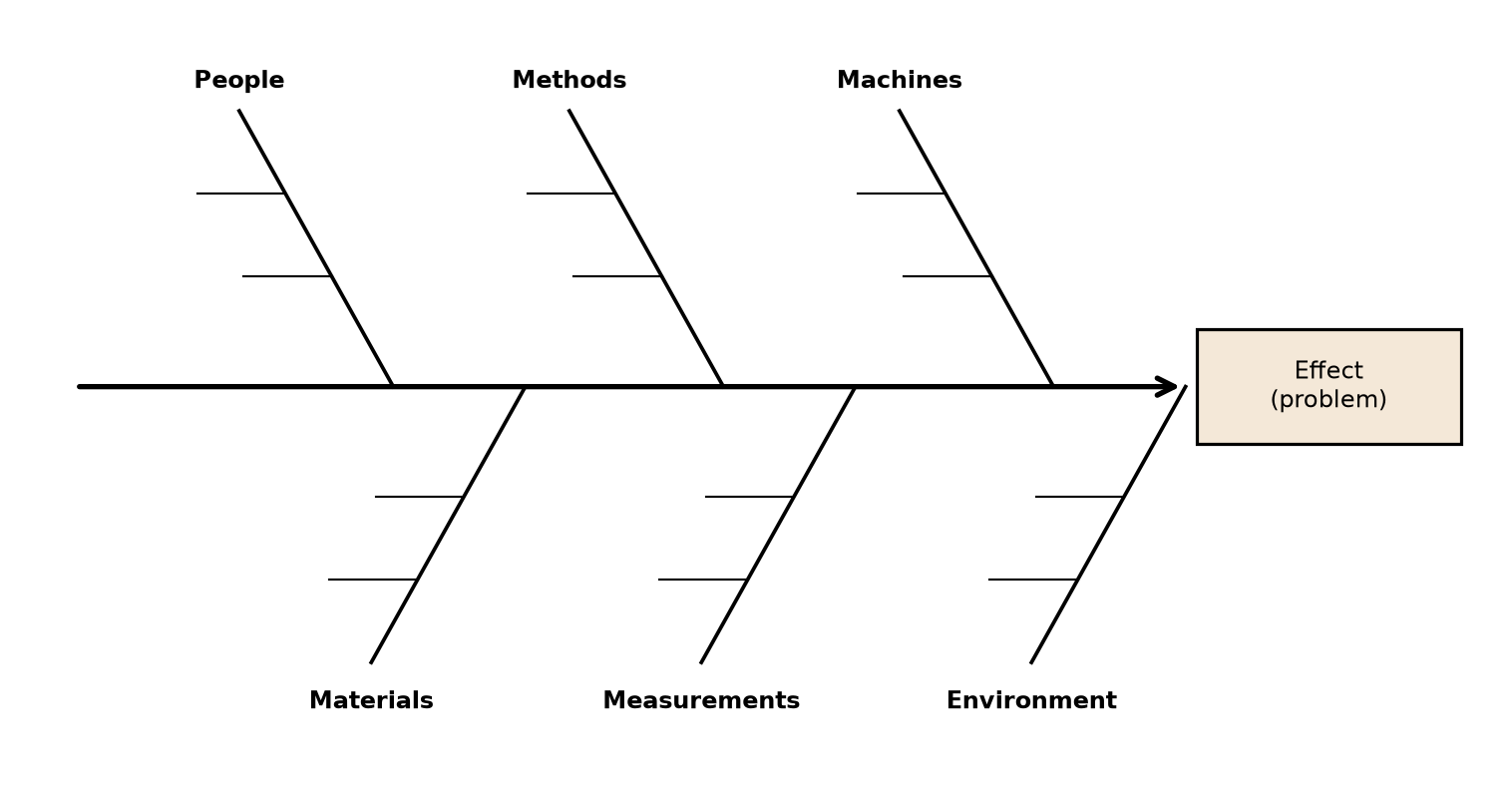
10.5.2 The “5-Why” Method
A helpful strategy to identify causes is the “5-why” method: ask “Why…?” five times in succession (five is just a rough number—more or less, depending on complexity); the method originates from the Toyota production system (Ohno 1988). An example:
- “Why did the robot stop?” → The circuit overloaded, causing a fuse to blow.
- “Why did the circuit overload?” → There was insufficient lubrication on the bearings, so they locked up.
- “Why was there insufficient lubrication?” → The oil pump is not circulating enough oil.
- “Why is the pump not circulating enough oil?” → The pump intake is clogged with metal shavings.
- “Why is the intake clogged?” → Because there is no filter on the pump.
This may sound simple, but in a complex setting (time pressure, pressure from management or customers), analyzing an issue with simple, structured methods is an effective way to make progress.
10.5.3 Focused Ion Beam (FIB)
The focused ion beam (FIB) is an extremely helpful technique to modify on-chip circuitry, by cutting connections and/or creating new on-chip connections (it can also create probe pads for micro-probing) (Giannuzzi and Stevie 2005):
- A FIB machine uses ions (e.g., Ga) to remove material from a sample by sputtering/milling, with a resolution down to about 10 nm.
- Using a reactive gas inside the vacuum chamber, FIB-assisted CVD can deposit structured layers of, e.g., tungsten, forming new electrical connections.
- Since the deposited layers are very thin, creating low-ohmic connections is difficult—so a cut is preferable to a new connection where possible.
FIB access is easiest on the top metal layers; nets that are candidates for a FIB modification should therefore be routed (at least for a short section) on top metal, away from dense wiring, and not be covered by metal fill. For flip-chip packages or dense metal stacks, FIB modifications from the backside of the thinned die are possible, but considerably more difficult.
10.5.4 Failure Analysis
Beyond electrical measurements at the pins, several physical failure-analysis techniques help to locate a fault on the die (a comprehensive overview is given in (Gandhi 2019)):
- Micro-probing: fine needles (or FIB-created probe pads) contact internal nodes to measure voltages and waveforms directly.
- Hot-spot detection: shorts, leaky junctions, and latched structures dissipate power locally, which can be localized by thermal imaging (e.g., lock-in thermography) or by liquid-crystal coatings changing their appearance with temperature.
- Photon emission microscopy: forward-biased junctions, MOSFETs in saturation, and oxide breakdown emit weak light (mostly in the infrared), which can be detected, also through the backside of the die.
- X-ray inspection and acoustic microscopy reveal package defects like broken bond wires, voids, or delamination non-destructively; afterwards, the die can be exposed by decapsulation and inspected optically or in a scanning electron microscope (SEM).
11 Simulation of Integrated Circuits
Circuit simulators are critically important for IC design, as the functionality and performance of an IC must be ensured before submitting the design to production—an expensive and lengthy process. Most circuit simulators today can be traced back to the SPICE software released in 1972 by UC Berkeley (whose source code was made public soon after), with SPICE2 (Nagel 1975) establishing the algorithms still in use today. This chapter is largely based on (Kundert 1995).
Excellent open-source simulators are available: GHDL for VHDL and iVerilog/Verilator for Verilog/SystemVerilog digital simulation, and ngspice VACASK, and Xyce for SPICE analog/mixed-signal simulation.
The documentation of VACASK is a good reading resource for learning how to set up and run simulations.
11.1 Formulating the Circuit Equations
For analog circuit simulation, the electrical network has to be formulated as a system of equations that the computer can solve. Most simulators use the modified nodal analysis (MNA) (Ho et al. 1975):Kirchhoff’s current law (KCL) is formulated for \(N-1\) nodes, using the node voltages as unknowns (one node serves as the reference or ground node, called node 0). For \(R\), \(L\), and \(C\), their characteristic equations are used:
\[ i_\mathrm{R} = \frac{1}{R} ( v_1 - v_2 ), \qquad i_\mathrm{C} = C \frac{ d( v_1 - v_2 )}{dt}, \qquad \frac{di_\mathrm{L}}{dt} = \frac{1}{L} (v_1 - v_2) \]
Voltage sources force a node voltage but contribute an unknown branch current; current sources force a branch current. The same holds for inductors, whose branch current is kept as an unknown so that their differential equation can be expressed.
Each element contributes only to the few matrix entries belonging to its terminals, so a simulator builds the matrix by adding a fixed pattern (the element stamp) for every element in the netlist. As a node typically connects to only a few elements, the resulting matrices are very sparse.
Note 6: MNA Example
Let us perform the modified nodal analysis for the simple circuit in Figure 90. As a first step, the voltage nodes are numbered, and the directions of the branch currents are fixed. The KCL equations are formulated for each node except the reference node (current flowing out counts positive):
Node \(v_1\): \(i_\mathrm{a} + i_\mathrm{b} = 0\), and node \(v_2\): \(-i_\mathrm{b} + i_\mathrm{c} - i_\mathrm{d} = 0\).
Next, the currents are expressed through the element equations. For node \(v_1\):
\[ i_\mathrm{a} + \frac{v_1 - v_2}{R_1} = 0 \]
and for node \(v_2\), using \(i_\mathrm{d} = I_\mathrm{g}\):
\[ -\frac{v_1 - v_2}{R_1} + \frac{v_2}{R_2} - I_\mathrm{g} = 0 \]
The current through the voltage source cannot be expressed by node voltages, so we keep it as an additional unknown and add the compensating equation \(v_1 - V_\mathrm{g} = 0\). Finally, everything is put into matrix form:
\[ \begin{bmatrix} \frac{1}{R_1} & -\frac{1}{R_1} & 1 \\ -\frac{1}{R_1} & \frac{1}{R_1} + \frac{1}{R_2} & 0 \\ 1 & 0 & 0 \end{bmatrix} \begin{bmatrix} v_1 \\ v_2 \\ i_\mathrm{a} \end{bmatrix} - \begin{bmatrix} 0 \\ I_\mathrm{g} \\ V_\mathrm{g} \end{bmatrix} = 0 \tag{66}\]
Equation 66 has the form \(\mathbf{G} \mathbf{x} - \mathbf{w} = 0\). Since the entries of \(\mathbf{G}\) are constant in this example, the solution is simply \(\mathbf{x} = \mathbf{G}^{-1} \mathbf{w}\). Note that \(\mathbf{G}\) must be invertible (\(\det \mathbf{G} \neq 0\)), otherwise no solution can be found—and this is also true inside circuit simulators (a typical cause is a floating node without a DC path to ground, or a loop of ideal voltage sources)! Simulators never compute \(\mathbf{G}^{-1}\) explicitly but solve the system by sparse LU factorization.
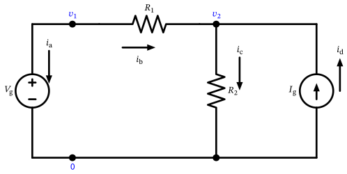
11.1.1 Controlled Sources
Voltage and current sources can also be controlled elements, like a voltage-controlled current source—such elements are needed, e.g., to model active devices like MOSFETs and BJTs:
- The addition of voltage-controlled elements (VCVS, VCCS) is a straightforward extension of the MNA, as the node voltages are already part of the equation system.
- The addition of current-controlled elements (CCVS, CCCS) requires sensing a branch current; conceptually, this is achieved by inserting a 0 V voltage source, which introduces an additional unknown branch current into the equation system that can then control the dependent source.
11.2 DC Simulation
The simulation of the dc operating point (.op in SPICE) is usually the first step in any circuit simulation; the dc sweep (.dc) repeats it while stepping a source value (or temperature), e.g., to obtain transfer characteristics. Before the circuit equations are derived, all capacitors are replaced by open circuits, and all inductors by short circuits. Some elements are nonlinear functions of voltage or current, leading to a nonlinear system of equations,
\[ \mathbf{G} \mathbf{x} + \mathbf{p}(\mathbf{x}) - \mathbf{w} = 0 \tag{67}\]
where \(\mathbf{p}(\mathbf{x})\) collects all nonlinear current and voltage relationships.
11.2.1 Solving Nonlinear Equations
The nonlinear circuit equations of the dc analysis are solved with the Newton-Raphson algorithm. Newton’s iterative method for solving a nonlinear equation \(f(x) = 0\) in a single variable starts with an initial guess \(x_0\) and repeatedly evaluates
\[ x_{n+1} = x_n - \left[ \frac{d}{dx} f(x_n) \right]^{-1} f(x_n) \]
The generalization to multiple variables involves the Jacobian matrix:
\[ \mathbf{x}_{n+1} = \mathbf{x}_n - \left[ \mathbf{J}(\mathbf{x}_n) \right]^{-1} \mathbf{F}(\mathbf{x}_n) \tag{68}\]
In circuit terms, each Newton-Raphson iteration replaces every nonlinear element by its linearization at the present solution estimate—a companion model consisting of a conductance (the derivative) and a current source—and then solves the resulting linear MNA system. Close to the solution, the method converges quadratically; far from it, the iteration can overshoot or diverge, so simulators limit the voltage change per iteration (e.g., across \(pn\) junctions).
11.2.2 Convergence
Note that circuits sometimes have more than one dc solution (consider a flip-flop!), and the dc solution computed by the simulator may even be an unstable one. The iterative algorithm needs a convergence criterion, i.e., when to stop the iteration; SPICE uses three parameters (for higher accuracy, tighten these values at the cost of simulation speed):
RELTOL: relative tolerance of voltages and currents from one iteration to the next; default 0.001 (0.1 %).VNTOL: absolute node-voltage tolerance; default 1 µV.ABSTOL: absolute branch-current tolerance; default 1 pA.
A non-converging dc simulation can be a serious issue, which tends to get worse with increasing circuit size. Things to try:
- The starting point of the Newton-Raphson iteration matters, so provide initial guesses for critical nodes using the
.nodesetstatement (in contrast to.ic, which forces an initial condition for the transient simulation). - Floating small resistances are critical for convergence and should be avoided; for probing currents, a 0 V voltage source is a better choice than a small resistor.
- Very-high-impedance nodes and strong nonlinearities (e.g., in diodes) may cause convergence issues. The simulator automatically places a conductance in parallel with such structures, controlled by the parameter
GMIN(default \(10^{-12}\), i.e., 1 TΩ)—which itself can cause accuracy issues, e.g., in sample-and-hold circuits. - Another method to achieve convergence is source stepping: slowly ramp the voltage and current sources from zero to their final values, using the result of each step as the starting point for the next (alternatively,
GMINstepping can be used).
11.3 AC Simulation
For the small-signal ac simulation (.ac in SPICE), the large-signal operating point is first calculated using the dc simulation. The circuit is then linearized around this operating point (the nonlinear elements are replaced by their small-signal conductances, which are the entries of the Jacobian from Equation 68), and the complex impedances of \(L\) and \(C\) are incorporated in a phasor analysis. The frequency is swept from \(f_\mathrm{min}\) to \(f_\mathrm{max}\), and for each frequency the complex linear matrix equations of the form
\[ \left[ \mathbf{G} + j \omega \mathbf{C} \right]\mathbf{x} - \mathbf{w} = 0 \tag{69}\]
are solved, where \(\mathbf{C}\) holds the capacitances and inductances (the latter in the rows of the inductor branch currents). Due to the linearization, the ac simulation can not show effects like distortion, clipping, or frequency translation! Also, use the ac simulation with care when evaluating the stability of circuits: stability is only shown for the selected operating point—in another operating point, the circuit may behave differently. For assessing the stability of feedback loops, breaking the loop by hand is error-prone (it disturbs the loading and the operating point); dedicated loop-gain methods like the one in (Tian et al. 2001) (available as stb analysis in Spectre) measure the loop gain without opening the loop.
11.3.1 Noise Simulation
The ac framework also provides the noise analysis (.noise in SPICE): small-signal noise sources are added to the circuit automatically (thermal noise for resistors; additionally shot noise and flicker noise for active devices). By computing the transfer function of each noise source to an output port (efficiently done for all sources at once using the adjoint network), the noise contributions are summed in power at the output, and dividing by the gain yields the input-referred noise. The contribution list per device is a valuable design aid to identify the dominant noise sources. Since .noise is based on .ac, nonlinear noise effects (as in mixers, oscillators, or sampled circuits) can not be simulated this way. For modeling purposes, a noiseless resistor is sometimes needed: it can be built from a VCCS, or by setting the resistor’s local temperature to 0 K if the simulator supports it.
11.4 Transient Simulation
In the transient analysis (.tran in SPICE), inductors and capacitors must be considered with their differential equations, so the circuit is described by a system of differential-algebraic equations (DAEs) of the general form
\[ \mathbf{C} \frac{d}{dt} \mathbf{x} + \mathbf{G} \mathbf{x} + \mathbf{p}(\mathbf{x}) - \mathbf{w}(t) = 0 \tag{70}\]
For solving the DAEs, the time-derivative operator is replaced by a discrete-time approximation, and the resulting finite-difference equations are solved one time point at a time. At each time point, this results in a nonlinear algebraic system just like in the dc analysis, which is solved by Newton-Raphson iteration (with the solution of the previous time point as a good starting guess).
11.4.1 Discrete-Time Integration Methods
The discrete-time approximations mostly used in circuit simulators are listed in Table 14 (with the time step \(\Delta T = t_{k+1} - t_k\)).
| Method | Approximation |
|---|---|
Forward Euler (FE) |
\(\frac{d}{dt}v(t_k) \approx \frac{1}{\Delta T} [ v(t_{k+1}) - v(t_k) ]\) |
Backward Euler (BE) |
\(\frac{d}{dt}v(t_{k+1}) \approx \frac{1}{\Delta T} [ v(t_{k+1}) - v(t_k) ]\) |
Trapezoidal rule (TR) |
\(\frac{d}{dt}v(t_{k+1}) \approx \frac{2}{\Delta T} [ v(t_{k+1}) - v(t_k) ] - \frac{d}{dt}v(t_{k})\) |
2nd-order backward difference (Gear2) |
\(\frac{d}{dt}v(t_{k+1}) \approx \frac{3}{2\Delta T} v(t_{k+1}) - \frac{2}{\Delta T} v(t_k) + \frac{1}{2\Delta T} v(t_{k-1})\) |
If the time steps are small enough, the approximation of the differential operator is adequate; circuit simulators change the time step dynamically during the simulation to trade off accuracy against simulation time. The step size is controlled by estimating the local truncation error of the integration method: the step is reduced when signals change quickly (and a time point is rejected if the error is too large), and enlarged when signals are smooth. If Newton-Raphson fails to converge at a time point, the step is reduced as well—repeated failure ends in the infamous “timestep too small” error. Regarding the choice of method:
FEis an explicit method and is numerically unstable for stiff circuits (with widely separated time constants, which is the normal case), unless the time step is tiny; therefore, it is not used in general-purpose circuit simulators.TRandGear2are the most heavily used integration methods in circuit simulation.- For a fixed time step, the most accurate method is
TR, followed byGear2. TRis overly sensitive to errors of previous time steps, so do not use it with a looseRELTOL!- For abrupt signal changes,
BEandTRadapt quickly, but beware of the artificial ringing introduced byTR. Gear2is efficient when simulating with tight tolerances or smooth waveforms.BE,TR, andGear2are stable on stiff circuits, butBEshows strong artificial numerical damping (TRshows none,Gear2weak damping).
Overall, Gear2 is a robust choice for most circuits. Note that simulator defaults differ: ngspice, for example, uses TR by default, and switches to Gear integration with .options method=gear (the order is set by maxord).
11.4.2 Using the Transient Simulation
Depending on the simulation task, the proper integration method should be selected, keeping potential numerical ringing and damping in mind when evaluating results. Some practical notes:
- Since no noise is modeled in the plain transient simulation, the startup of oscillators or bi-stable circuits can be inhibited—if so, a start-up pulse or an initial condition is required!
- The transient simulation can be an effective fallback to find a dc operating point if
.opdoes not converge, by slowly ramping all dc sources from zero to their final values. - If high accuracy is needed, tighten the tolerance parameters (
RELTOL,VNTOL,ABSTOL) and limit the maximum time step (TMAX). - Nonlinearity is inherently captured in
.tran—but noise is not! - When applying an FFT to transient results, make sure that all transients have settled (use
TSTARTto delay the recording of the output). As the time points are not equidistant, the waveform is interpolated before the FFT; limitTMAXaccordingly, and use coherent sampling or a window function to avoid spectral leakage.
11.5 Advanced Simulation Modes
Beyond the basic analyses (.dc, .ac, .noise, .tran), advanced circuit simulators offer analyses that capture large-signal noise effects, including frequency conversion and time-varying bias points:
- In the transient noise simulation, the noise sources are modeled as random signals in the time domain and added to the circuit (in
ngspice, e.g., by usingtrnoisesources, or inVACASKby using the transient noise analysis). As the noise bandwidth is linked to the time step, such simulations are slow and require many runs or long simulation times for statistically meaningful results. - For RF simulation, there is a large discrepancy between the baseband (low) frequencies and the high carrier frequency, which makes the standard transient simulation extremely time-consuming (a small time step is dictated by the carrier, but a long simulation time by the modulation). For these cases, special methods like harmonic balance or shooting-Newton have been developed; see (Kundert 1999) for an introduction. In the open-source domain,
XyceandVACASKoffer a harmonic-balance analysis.
Commercial RF simulators (e.g., Cadence SpectreRF) offer a whole family of such analyses: periodic steady-state in the time domain (pss, with pac, pstb, pnoise, pxf, psp) for circuits with one periodic excitation; quasi-periodic steady-state (qpss, …) for circuits operating on multiple fundamental frequencies; and harmonic balance in the frequency domain (hb, hbac, hbnoise, …) for the natural inclusion of \(S\)-parameters and frequency conversion. Additional analyses cover device matching (dcmatch, acmatch), stability (stb), pole-zero (pz), \(S\)-parameters (sp), and envelope following (envlp).
11.6 Device Models
To include active devices (diodes, BJTs, MOSFETs) in the circuit simulation, numerically efficient compact models have been developed and implemented in the simulators. Exemplary MOSFET model families (dozens have been developed over time):
- The SPICE level-1 model (the most basic model with a minimum number of parameters).
- The BSIM family (mainly BSIM3 and BSIM4 for planar bulk CMOS, BSIM-CMG for FinFETs), the widespread industry standard.
- The PSP model, well suited for analog/mixed-signal/RF design.
The standard models are maintained under the umbrella of the Compact Model Coalition (CMC) and are distributed as Verilog-A code. Open-source simulators use them via a Verilog-A compiler like OpenVAF, whose compiled models are loaded by ngspice (through the OSDI interface) and VACASK.
For modeling production variations, corner and Monte-Carlo model sets are provided by the foundry (see Section 10.2).
11.6.1 SPICE Level-1
The original MOSFET model implemented in SPICE, also known as the Shichman-Hodges model, is based on the following equations (with \(K_\mathrm{p} = \mu C'_\mathrm{ox}\) and \(V_\mathrm{th}= V_\mathrm{th0} + \gamma ( \sqrt{2 \Phi_\mathrm{B}- V_\mathrm{BS} } - \sqrt{2 \Phi_\mathrm{B}} )\)):
\[ I_\mathrm{D}= \frac{1}{2} K_\mathrm{p} \frac{W}{L - 2 L_\mathrm{D}} \left[ 2 (V_\mathrm{GS}- V_\mathrm{th}) V_\mathrm{DS}- V_\mathrm{DS}^2 \right] ( 1 + \lambda V_\mathrm{DS}) \quad \text{(triode)} \]
\[ I_\mathrm{D}= \frac{1}{2} K_\mathrm{p} \frac{W}{L - 2 L_\mathrm{D}} (V_\mathrm{GS}- V_\mathrm{th})^2 ( 1 + \lambda V_\mathrm{DS}) \quad \text{(saturation)} \]
This model includes neither subthreshold conduction nor any short-channel effects, so it should not be used below roughly 4 µm gate length! In addition, since its \(C_\mathrm{GS}\) changes abruptly between the saturation and triode regions, computation algorithms often experience convergence difficulties with it.
11.6.2 BSIM3 and BSIM4
The Berkeley BSIM models are the industry standard since version 3 (especially BSIM3v3) (Cheng and Hu 1999). They are source-referenced, threshold-voltage-based models and properly capture effects like mobility reduction, velocity saturation, DIBL, non-uniform doping, poly depletion, geometric scaling, and extrinsic parasitics (often modeled by embedding the intrinsic device in a subcircuit). BSIM4 adds gate current, gate-induced drain/source leakage, and improved flicker-noise modeling. The main disadvantage of the BSIM models is a lack of symmetry around \(V_\mathrm{DS}= 0\), which can be critical when a MOSFET operates as an analog switch with small \(V_\mathrm{DS}\). This is fixed in the charge-based successor model BSIM-BULK (formerly BSIM6).
11.6.3 PSP
The PSP model (Gildenblat et al. 2006) is a symmetric, surface-potential-based model, created by merging the SP model (Pennsylvania State University) and MOS Model 11 (Philips), and selected by the CMC as an industry standard. It accurately models \(g_\mathrm{m}/I_\mathrm{D}\) in all operating regions as well as distortion—especially at small \(V_\mathrm{DS}\), where BSIM has issues. In addition, PSP provides detailed and accurate noise models (including induced gate noise and the correlation between gate and drain noise) and takes non-quasi-static (NQS) effects into account. IHP SG13 uses PSP models for the core and I/O MOSFETs.
11.6.4 NQS Effects
The quasi-static assumption underlying most compact models is that the terminal voltages change slowly enough for the channel charge to follow instantaneously. If this assumption is violated (e.g., in RF operation), NQS effects must be considered. Following (Bagheri and Tsividis 1985), a simple first-order model of the NQS effect is an additional gate resistance of
\[ R_\mathrm{G,nqs} = \frac{1}{5 g_\mathrm{m}} \tag{71}\]
11.7 Digital Simulation
Digital simulation is much less numerically intensive than analog simulation, as the signal values are discrete and the timing is event-driven. The signal values used in digital simulation are 0 (logic zero), 1 (logic one), X (unknown/undefined), and Z (high-impedance/tri-state). Transitions occur only at discrete points in time (driven by input events and the clock), considering the delays of the logic elements and the wiring.
Two main simulator types are in use:
- Event-driven simulators (like
GHDLandiVerilog) evaluate a logic element only when one of its inputs changes, and support the full language semantics including delays andX/Zstates. After synthesis and place-and-route, a gate-level simulation with delays back-annotated from an SDF file is possible, although timing is primarily verified by static timing analysis. - Cycle-based simulators (like
Verilator) compile the design into a C++ model that is evaluated once per clock cycle, typically with two-state (0/1) logic and without delays; this is dramatically faster and well suited for large synchronous designs and long test runs (e.g., booting software on a CPU core).
An intermediate method between analog and digital simulation is timing simulation: strongly simplified MOSFET models avoid the solution of nonlinear systems, matrix operations are minimized, and forward-Euler integration is used—trading accuracy for speed.
11.8 Mixed-Signal Simulation
Simulating a large mixed-signal circuit (e.g., a complex SoC combining analog circuits and digital blocks) may require a coupled mixed-signal simulation, where parts of the design run in an analog circuit simulator and other parts in a digital simulator (ngspice offers an integrated event-driven digital simulation with XSPICE, and can co-simulate Verilog code compiled by Verilator or iVerilog through its d_cosim element):
- An all-analog (transistor-level) simulation of the digital part is possible but usually too time-consuming.
- For further speed-up, some analog circuits can be replaced by behavioral descriptions (e.g., in Verilog-AMS or VHDL-AMS).
At the interfaces between the analog and digital partitions, interface elements (IEs) are inserted (manually or automatically), converting between the signal representations:
- Digital → analog (D2A): the IE is a voltage source with optional output resistance and finite transition times; the logic
0/1levels are mapped to voltage levels. - Analog → digital (A2D): the IE is a comparator with adjustable thresholds for
0and1(andXin between).
12 Project Management
Designing an integrated circuit is a complex process with many dependencies and interrelated tasks. Therefore, careful project planning is essential to ensure that all activities are coordinated and completed successfully.
A project plan, in its simplest form, is an attempt at a timetable for all the activities which make up a project; as a minimum, it sets out “how,” “who does what,” and “when.” A more sophisticated plan also states “at which quality level,” “at what cost,” and “with which resources.” Planning is an iterative process, and the amount of detail included varies over time. The project plan is prepared and tracked by the project management, with the advice and assistance of the project sponsor, customer, project team, and other stakeholders. General introductions to the field are (Project Management Institute 2021) and (Kerzner 2022).
IC projects have a few properties that make planning both harder and more important than in many other engineering disciplines:
- Tapeout is irreversible. Once the layout database is sent to the foundry, no change is possible until silicon returns, typically after two to four months of fabrication, packaging, and shipping. A bug found afterward costs a re-spin, i.e., new masks (see Section 7.2) and another full fabrication cycle.
- Deadlines are fixed from the outside. Prototypes are often fabricated on a multi-project wafer (MPW) shuttle with a small number of fixed tapeout dates per year; missing a shuttle delays the project by months, not by days.
- Verification dominates. A large and growing fraction of the effort is not spent on designing but on verifying the design. Nevertheless, industry surveys show that only a minority of IC/ASIC projects achieve first-silicon success, and that most projects are behind schedule (Foster 2024).
Good project management cannot remove technical risk, but it makes the risk visible early and leaves enough time and budget to deal with it.
12.1 Goals and Constraints
Every project is bounded by the triple constraint of scope (what is delivered, including its quality), time, and cost. These three are coupled: adding functionality to an IC under a fixed tapeout date increases cost (more engineers, more licenses) or lowers quality (less verification); a fixed team and scope define the earliest realistic tapeout date. The project management has to make these trade-offs explicit and agree on them with the sponsor—a plan that silently assumes all three can be held at once is not a plan.
Project goals should be formulated so that everybody can decide whether they are met. A widely used checklist is SMART: goals are specific, measurable, achievable, relevant, and time-bound (in the original proposal (Doran 1981), the letters stood for specific, measurable, assignable, realistic, and time-related). “Design a low-power ADC” is not a goal; “tape out a 10 bit SAR ADC with \(\geq 9.5\) bit ENOB at 1 MS/s and \(\leq 100\,\mu\text{W}\) on the IHP SG13G2 shuttle of March” is.
For an IC, the goals are condensed into the specification. The most expensive changes are those made late, as each change ripples through design, layout, verification, test program, and documentation. Therefore, the specification is reviewed and frozen at an early milestone; later changes are still possible, but go through a formal change request that assesses the impact on schedule and cost before the change is accepted.
12.2 Project Phases
The technical work of an IC project follows the V-model (Forsberg and Mooz 1991): on the descending branch, the system is decomposed from the specification over the architecture into blocks, which are designed and laid out; on the ascending branch, the blocks are verified and integrated, and the complete chip is verified against the specification. Each level of the descending branch defines the test criteria for the same level on the ascending branch—the block specification is the reference for block verification, and the chip specification the reference for silicon characterization. In contrast to software, the tip of the V contains the tapeout and fabrication, which cannot be iterated quickly.
Table 15 lists typical phases, each concluded by a milestone that marks a decision point (a gate) at which the results are reviewed before the next phase is started.
| Phase | Main activities | Milestone (gate) |
|---|---|---|
| Definition | Requirements, feasibility, technology choice, budget | Specification and project plan frozen |
| Architecture | System modeling, block partitioning, block specifications, test and debug concept | Architecture review |
| Design | Schematic/RTL design, block simulation and verification | Design review |
| Layout | Floor plan, block layout, P&R, top-level assembly, PEX simulation | Layout review |
| Tapeout | DRC/LVS/ERC sign-off, final verification, database release | Tapeout |
| Fabrication | Test PCB, test program, lab setup (in parallel to the fab run) | Silicon arrival |
| Evaluation | Functional test, characterization, debug | Evaluation report |
| Qualification | Reliability tests, production test release (products only) | Release to production |
For the design phase itself, iterative (“agile”) ways of working have proven useful, especially for RTL and software, where regression tests can be run automatically. The hard gate at tapeout, however, remains; iterations have to converge before it.
12.3 Statement of Work
Project goals are often collected in a statement of work (SOW): specifications, cost, quality, deadlines, and project deliverables, plus a detailed description of the work (possibly in the form of a legal contract), containing:
- Introduction/background
- Technical description
- Timeline and milestones
- Payment details
- Client expectations
For the individual tasks within the project, the SOW defines the estimated duration, resources, and cost; measures of performance (what are suitable indicators?); risks and uncertainties; and the reporting procedure. The deliverables (milestones) are captured as a list of items or activities needed to meet the defined goals, together with when and how each item must be delivered. Equally important is what is not part of the work (e.g., “package qualification is not included”), as unclear boundaries are a frequent source of conflict with customers and partners.
12.4 Work Breakdown Structure
To arrive at the individual work packages for the SOW, it is useful to employ a work breakdown structure (WBS) to derive the tasks iteratively: the WBS breaks the project down into several deliverables; each deliverable consists of work packages (WPs), and each work package can consist of several work units, as shown in Figure 91.
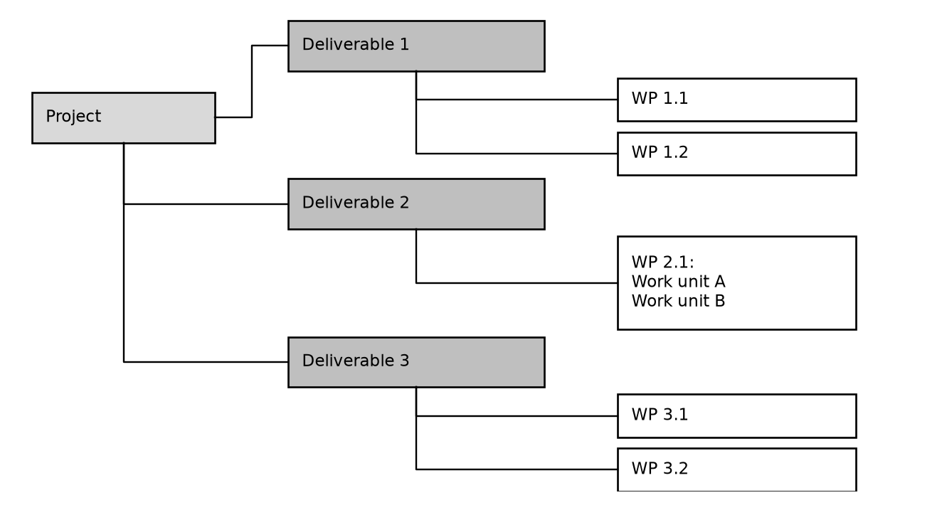
A few rules help to create a useful WBS (Project Management Institute 2019):
- 100 % rule: the WBS contains the complete work of the project—no more and no less—and the children of each element add up to 100 % of the parent’s work. Work that does not appear in the WBS will not be planned, staffed, or budgeted.
- Deliverable-oriented: the elements are outcomes (e.g., “bandgap reference, verified layout”), not activities or departments. This makes progress measurable.
- Mutually exclusive: no work is contained in two elements, otherwise it is counted twice.
- Adequate granularity: a work package is small enough to be estimated and assigned to one responsible person, and large enough to be worth tracking; a common heuristic is a size between one day and a few weeks of effort.
Each work package is described in a short WBS dictionary entry: responsible person, content, inputs, deliverables, effort estimate, and completion criterion. The completion criterion (“done” means, e.g., “schematic reviewed, all corners and Monte-Carlo simulations pass, results documented”) prevents the familiar situation where a task stays “90 % complete” for weeks.
In IC projects, a WBS built only from the circuit blocks misses a large part of the work. Typically forgotten are top-level verification and mixed-signal simulations, the pad ring and ESD concept (see Section 9), package selection and bonding diagram (see Section 5), test PCB and test program (see Section 6.4), tapeout checks, documentation, and project management itself.
12.5 Effort Estimation
Estimates are needed for every work package. It is important to distinguish effort (person-days of work) from duration (calendar time): a work package with 10 person-days of effort does not finish in two weeks if the responsible designer also supports the lab and attends meetings. Plan with a realistic availability of 60 % to 80 % of the working time for project work.
Single-value estimates hide the uncertainty. The three-point estimate of the PERT method (Malcolm et al. 1959) asks for an optimistic (\(t_o\)), a most likely (\(t_m\)), and a pessimistic (\(t_p\)) duration, and approximates the expected duration and its standard deviation by
\[ t_e = \frac{t_o + 4 t_m + t_p}{6}, \qquad \sigma_t = \frac{t_p - t_o}{6}. \tag{72}\]
For a bandgap reference with \(t_o = 5\) days, \(t_m = 8\) days, and \(t_p = 17\) days, the expected duration is \(t_e = 9\) days with \(\sigma_t = 2\) days. Note that \(t_e > t_m\): the duration distribution of engineering tasks is skewed, since there are many more ways for a task to take longer than planned than to finish early. For a sequence of independent tasks, the expected durations add up, and so do the variances \(\sigma_t^2\).
Estimates improve with historical data (how long did the last PLL take?), with bottom-up estimation by the people doing the work, and when the pessimistic value explicitly includes the rework after a failed review. Three well-known observations should be kept in mind:
- Brooks’s law (Brooks, Jr. 1995): “Adding manpower to a late software project makes it later.” New team members need training by the experienced ones, and the communication overhead grows with the number of pairs, \(n(n-1)/2\), in a team of \(n\) persons. The same holds for IC projects.
- Parkinson’s law: work expands to fill the time available. Generous buffers hidden in every task are consumed; it is better to estimate tasks realistically and to hold an explicit project buffer before the tapeout.
- Verification effort is regularly underestimated. It is not a phase at the end, but runs in parallel to the design from the first block on (see Section 11 and Section 10.2).
12.6 Scheduling
A Gantt chart is one way to visualize and maintain a project schedule; it is usually updated regularly during the project. The elements of a Gantt chart are:
- Task names
- Start/finish dates or durations of the tasks
- Dependency relationships between the tasks
- Lag relationships (start-to-start, finish-to-start, etc.)
- Task responsibilities (who does it)
- Required resources
Figure 92 shows an exemplary Gantt chart with task groups, task progress, a milestone, and dependencies.
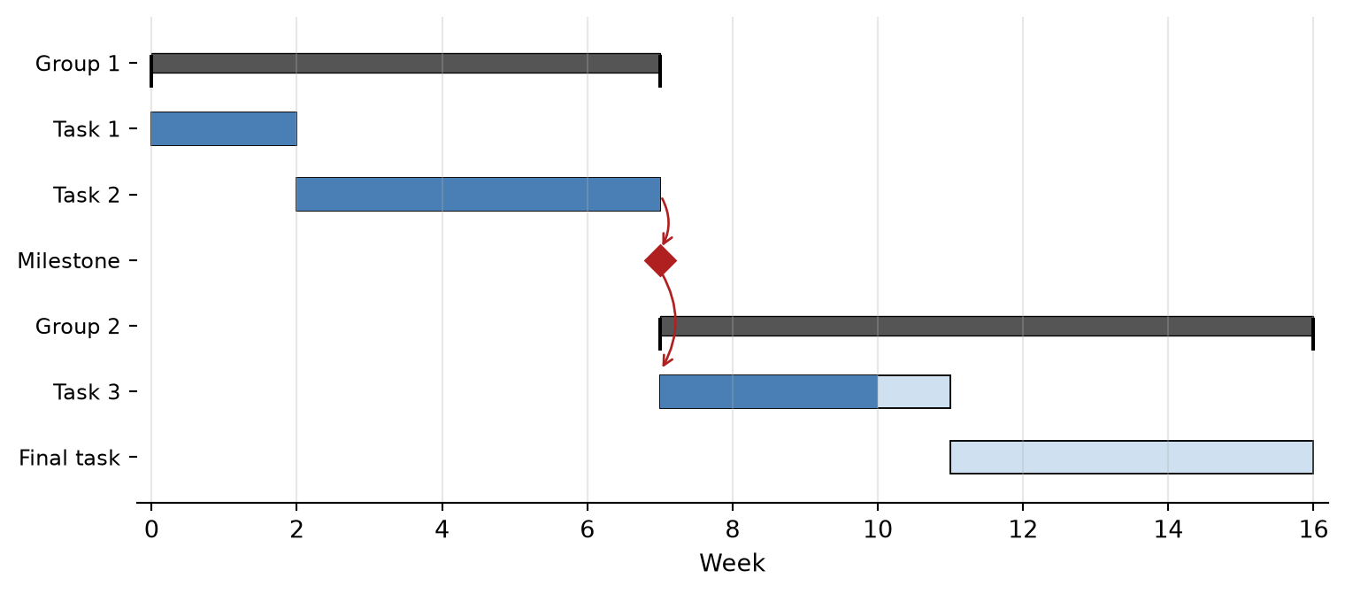
The Gantt chart shows when tasks happen, but not directly which tasks determine the end date. This is answered by the critical path method (CPM) (Kelley, Jr. and Walker 1959). In a forward pass through the dependency network, the earliest start (ES) and earliest finish (EF \(=\) ES \(+\) duration) of each task are calculated, where ES is the maximum EF of all predecessors. In a backward pass from the project end, the latest finish (LF) and latest start (LS \(=\) LF \(-\) duration) are calculated, where LF is the minimum LS of all successors. The difference
\[ \text{Float} = \text{LS} - \text{ES} = \text{LF} - \text{EF} \tag{73}\]
is the time by which a task can slip without delaying the project. Tasks with zero float form the critical path; any delay on it delays the tapeout.
Table 16 shows a simplified mixed-signal chip project (durations in weeks). The critical path is A–B–D–F–G with a total duration of 16 weeks, i.e., the analog design and layout set the tapeout date. The digital branch C–E has a float of 4 weeks; accelerating the digital work does not help the schedule at all, whereas every week gained in the analog design is a week gained for the project.
| Task | Description | Duration | Predecessors | ES | EF | LS | LF | Float |
|---|---|---|---|---|---|---|---|---|
| A | Specification and architecture | 2 | – | 0 | 2 | 0 | 2 | 0 |
| B | Analog design | 6 | A | 2 | 8 | 2 | 8 | 0 |
| C | Digital RTL design and verification | 4 | A | 2 | 6 | 6 | 10 | 4 |
| D | Analog layout | 4 | B | 8 | 12 | 8 | 12 | 0 |
| E | Digital synthesis and P&R | 2 | C | 6 | 8 | 10 | 12 | 4 |
| F | Top-level integration and verification | 3 | D, E | 12 | 15 | 12 | 15 | 0 |
| G | Sign-off and tapeout | 1 | F | 15 | 16 | 15 | 16 | 0 |
When the tapeout date is fixed by a shuttle, the schedule is best built backward from this date: the latest finish of the last task is the shuttle deadline, and a negative float in the backward pass immediately shows that the plan is not feasible and scope or resources have to be adjusted—before the project starts, not two weeks before the tapeout. Keep in mind that the critical path can move during the project, e.g., when the digital branch runs into problems and consumes its float, and that the CPM assumes unlimited resources: if B and C are done by the same designer, they cannot run in parallel.
12.7 Roles and Responsibilities
Each work package needs exactly one person who is accountable for its completion. A responsibility assignment matrix, also called RACI matrix, maps the work packages to the team members, stating who is responsible (does the work), accountable (owns the result and approves it; exactly one per task), consulted (gives input before), and informed (is notified after). Table 17 shows an example.
| Work package | Project lead | Analog designer | Digital designer | Layout | Test engineer |
|---|---|---|---|---|---|
| Chip specification | A | R | R | C | C |
| Bandgap reference | I | A/R | – | C | C |
| Digital control (RTL) | I | C | A/R | – | C |
| Top-level layout | I | C | C | A/R | I |
| Tapeout sign-off | A | R | R | R | I |
| Test program | I | C | C | – | A/R |
The matrix makes gaps (a task without an owner) and overloads (one person responsible for everything critical) visible. The latter is a common risk in small IC teams, where a single expert is often the only one who knows a block well enough to debug it.
12.8 Risk Management
A risk is an uncertain event that, if it occurs, affects the project goals. Risk management is a continuous loop of identifying risks, assessing them, planning responses, and monitoring them throughout the project (Project Management Institute 2021). Risks are collected in a risk register; each risk is rated by its probability of occurrence \(P\) and its impact \(I\) (e.g., both on a scale from 1 to 5), and the product \(P \cdot I\) is used to prioritize. The possible responses are to avoid the risk (change the plan so that it cannot occur), mitigate it (reduce \(P\) or \(I\)), transfer it (e.g., buy a silicon-proven IP block with a warranty), or accept it (with a contingency plan and budget reserve).
Typical risks in IC projects and possible responses are listed in Table 18.
| Risk | \(P\) | \(I\) | \(P \cdot I\) | Response |
|---|---|---|---|---|
| Functional bug found after tapeout | 3 | 5 | 15 | Mitigate: verification plan with coverage metrics, reviews, spare cells and metal-fix options (see Section 10.5) |
| Late or immature PDK or IP | 3 | 4 | 12 | Mitigate: early test chip, qualified IP only, freeze PDK version |
| Key designer leaves or is unavailable | 2 | 5 | 10 | Mitigate: reviews, documentation, second person per critical block |
| Performance missed due to layout parasitics | 3 | 3 | 9 | Mitigate: parasitic estimates in early simulations, PEX simulations (see Section 10.3) |
| Shuttle date missed | 2 | 4 | 8 | Avoid: backward scheduling with buffer; accept: identify alternative shuttle |
| Specification change by customer | 2 | 3 | 6 | Mitigate: specification freeze and change-request process |
The largest risk of an IC project, a non-functional first silicon, is best addressed with a combination of measures: thorough verification, design reviews by colleagues who did not design the block, a tapeout checklist, test chips for new circuit concepts, built-in observability and programmability (see Section 10), and a schedule and budget that already contain a realistic probability of a metal re-spin.
12.9 Reviews and Tapeout Checklist
Design reviews are the most effective and cheapest method to find errors before they reach silicon. A review is scheduled at each gate (Table 15), prepared with documents distributed in advance, attended by experienced engineers who are not the authors of the design, and concluded with a written list of action items, each with an owner and a due date. The author presents the design intent, the specification versus simulation results over all corners, and the open issues; the reviewers ask the “what if” questions—What happens at power-up? What if the reference is not yet settled? What if the digital control sends an illegal state?
Right before the tapeout, a tapeout checklist ensures that nothing is forgotten under time pressure. The items are collected over many projects and grow with every lesson learned; typical entries are:
- DRC, LVS, ERC, antenna, and density checks clean on the final database, all waivers documented and approved by the foundry (see Section 4.7)
- Post-layout (PEX) simulations of all critical blocks over corners and temperature (see Section 10.2)
- ESD and latch-up checks, pad ring and bonding diagram matched to the package (see Section 9 and Section 5)
- Seal ring, chip ID/revision marking, alignment and test structures present
- Top-level netlist and layout versions tagged in the version control system; the final GDSII checksum recorded
- Test concept and test PCB ready to start in parallel to the fabrication (see Section 6.4)
12.10 Tracking and Control
A plan is only useful if the actual progress is regularly compared against it. Short, regular status meetings (weekly in most IC teams) track the progress of the work packages, the open action items, and the top risks. Progress should be measured by completed deliverables with a clear completion criterion (Section 12.4), not by the fraction of time spent.
A quantitative method that combines schedule and cost is earned value management (EVM) (Project Management Institute 2021). At a status date, the planned value (PV) is the budget of the work scheduled until this date, the earned value (EV) is the budget of the work actually completed, and the actual cost (AC) is what has actually been spent. The schedule and cost performance indices
\[ \text{SPI} = \frac{\text{EV}}{\text{PV}}, \qquad \text{CPI} = \frac{\text{EV}}{\text{AC}} \tag{74}\]
show a delay for SPI \(< 1\) and a cost overrun for CPI \(< 1\). For example, if 40 person-weeks of work were planned until today, work worth 32 person-weeks has been completed, and 45 person-weeks have been spent, then SPI \(= 0.8\) and CPI \(\approx 0.71\): the project is late and each completed work package costs more than estimated—a trend that rarely corrects itself without action.
A simple and popular visualization in European companies is the milestone trend analysis (MTA): at every reporting date, the currently forecast date of each milestone is plotted. A horizontal line indicates a stable forecast, a rising line a milestone that keeps slipping—usually an early warning long before the milestone is officially missed.
The technical data of the project need the same discipline: all design data (schematics, RTL, layouts, testbenches, scripts) are kept under version control, open issues are tracked in an issue tracker, and automated regression simulations show whether a change has broken something that worked before. Changes after the specification freeze go through the change-request process (Section 12.1). After the project, a short lessons-learned session collects what went well and what should be done differently; its results update the estimation data and the tapeout checklist for the next project.
12.11 Team and Communication
In the end, projects are carried out by people. Conway’s law (Conway 1968) states that organizations design systems whose structure mirrors their own communication structure. For ICs, this is visible at the interfaces between analog, digital, layout, and test teams: an interface between blocks that is not also an interface between people who talk regularly is a likely place for a bug. Interface specifications (pin lists, signal levels, timing, power-up sequence) should therefore be written down, owned, and reviewed by both sides.
Productive design work requires long, uninterrupted periods of concentration; frequent context switches between projects and meetings reduce the effective capacity much more than the time spent in them suggests (DeMarco and Lister 2013). A good project manager protects the team from unnecessary interruptions, resolves blocking issues quickly, and communicates bad news early—a delay announced three months before the tapeout leaves options, one announced three days before does not.
References
Afzali-Kusha, Ali, Makoto Nagata, Nishath K. Verghese, and David J. Allstot. 2006. “Substrate Noise Coupling in SoC Design: Modeling, Avoidance, and Validation.” Proceedings of the IEEE 94 (12): 2109–38. https://doi.org/10.1109/JPROC.2006.886029.
Allen, Phillip E., and Douglas R. Holberg. 2012. CMOS Analog Circuit Design. 3rd ed. Oxford University Press.
Amerasekera, Ajith, and Charvaka Duvvury. 2002. ESD in Silicon Integrated Circuits. 2nd ed. Wiley.
Bagheri, Mehran, and Yannis Tsividis. 1985. “A Small Signal Dc-to-High-Frequency Nonquasistatic Model for the Four-Terminal MOSFET Valid in All Regions of Operation.” IEEE Transactions on Electron Devices 32 (11): 2383–91.
Bhunia, Swarup, and Mark Tehranipoor. 2018. Hardware Security: A Hands-on Learning Approach. Morgan Kaufmann.
Brooks, Jr., Frederick P. 1995. The Mythical Man-Month: Essays on Software Engineering. Anniversary. Addison-Wesley.
Cheng, Yuhua, and Chenming Hu. 1999. MOSFET Modeling & BSIM3 User’s Guide. Kluwer Academic Publishers.
Conway, Melvin E. 1968. “How Do Committees Invent?” Datamation 14 (4): 28–31.
Craninckx, Jan, and Michiel S. J. Steyaert. 1995. “A 1.8-GHz CMOS Low-Phase-Noise Voltage-Controlled Oscillator with Prescaler.” IEEE Journal of Solid-State Circuits 30 (12): 1474–82.
Deal, Bruce E., and Andrew S. Grove. 1965. “General Relationship for the Thermal Oxidation of Silicon.” Journal of Applied Physics 36 (12): 3770–78.
DeMarco, Tom, and Timothy Lister. 2013. Peopleware: Productive Projects and Teams. 3rd ed. Addison-Wesley.
Dennard, Robert H., Fritz H. Gaensslen, Hwa-Nien Yu, V. Leo Rideout, Ernest Bassous, and Andre R. LeBlanc. 1974. “Design of Ion-Implanted MOSFET’s with Very Small Physical Dimensions.” IEEE Journal of Solid-State Circuits 9 (5): 256–68.
Doran, George T. 1981. “There’s a S.M.A.R.T. Way to Write Management’s Goals and Objectives.” Management Review 70 (11): 35–36.
Forsberg, Kevin, and Harold Mooz. 1991. “The Relationship of System Engineering to the Project Cycle.” Proceedings of the First Annual Symposium of the National Council on Systems Engineering (NCOSE), 57–65. https://doi.org/10.1002/j.2334-5837.1991.tb01484.x.
Foster, Harry D. 2024. 2024 Siemens EDA and Wilson Research Group IC/ASIC Functional Verification Trend Report. White Paper. Siemens Digital Industries Software.
Gajski, Daniel D., and Robert H. Kuhn. 1983. “Guest Editors’ Introduction: New VLSI Tools.” Computer 16 (12): 11–14. https://doi.org/10.1109/MC.1983.1654264.
Gandhi, Tejinder, ed. 2019. Microelectronics Failure Analysis Desk Reference. ASM International.
Giannuzzi, Lucille A., and Fred A. Stevie, eds. 2005. Introduction to Focused Ion Beams: Instrumentation, Theory, Techniques and Practice. Springer. https://doi.org/10.1007/b101190.
Gildenblat, Gennady, Xin Li, Weimin Wu, et al. 2006. “PSP: An Advanced Surface-Potential-Based MOSFET Model for Circuit Simulation.” IEEE Transactions on Electron Devices 53 (9): 1979–93.
Goto, Ken-ichi et al. 2003. “High Performance 25 nm Gate CMOSFETs for 65 nm Node High Speed MPUs.” IEEE International Electron Devices Meeting (IEDM).
Hastings, Alan. 2006. The Art of Analog Layout. 2nd ed. Prentice Hall.
Ho, Chung-Wen, Albert E. Ruehli, and Pierce A. Brennan. 1975. “The Modified Nodal Approach to Network Analysis.” IEEE Transactions on Circuits and Systems 22 (6): 504–9. https://doi.org/10.1109/TCS.1975.1084079.
Hu, Chenming. 2010. Modern Semiconductor Devices for Integrated Circuits. Pearson.
Ishikawa, Kaoru. 1976. Guide to Quality Control. Asian Productivity Organization.
Kahng, Andrew B., Jens Lienig, Igor L. Markov, and Jin Hu. 2022. VLSI Physical Design: From Graph Partitioning to Timing Closure. 2nd ed. Springer.
Kelley, Jr., James E., and Morgan R. Walker. 1959. “Critical-Path Planning and Scheduling.” Proceedings of the Eastern Joint IRE-AIEE-ACM Computer Conference, 160–73. https://doi.org/10.1145/1460299.1460318.
Ker, Ming-Dou, Tung-Yang Chen, Chung-Yu Wu, and Hun-Hsien Chang. 2000. “ESD Protection Design on Analog Pin with Very Low Input Capacitance for High-Frequency or Current-Mode Applications.” IEEE Journal of Solid-State Circuits 35 (8): 1194–99. https://doi.org/10.1109/4.859509.
Ker, Ming-Dou, and Che-Hao Chuang. 2002. “ESD Protection Circuits with Novel MOS-Bounded Diode Structures.” IEEE International Symposium on Circuits and Systems (ISCAS) 5: V-533-V-536. https://doi.org/10.1109/ISCAS.2002.1010758.
Ker, Ming-Dou, Jeng-Jie Peng, and Hsin-Chin Jiang. 2001. “ESD Test Methods on Integrated Circuits: An Overview.” IEEE International Conference on Electronics, Circuits and Systems (ICECS) 2: 1011–14. https://doi.org/10.1109/ICECS.2001.957647.
Kerzner, Harold. 2022. Project Management: A Systems Approach to Planning, Scheduling, and Controlling. 13th ed. Wiley.
Kinget, Peter R. 2005. “Device Mismatch and Tradeoffs in the Design of Analog Circuits.” IEEE Journal of Solid-State Circuits 40 (6): 1212–24. https://doi.org/10.1109/JSSC.2005.848021.
Kundert, Kenneth S. 1995. The Designer’s Guide to SPICE and Spectre. Kluwer Academic Publishers.
Kundert, Kenneth S. 1999. “Introduction to RF Simulation and Its Application.” IEEE Journal of Solid-State Circuits 34 (9): 1298–319.
Malcolm, D. G., J. H. Roseboom, C. E. Clark, and W. Fazar. 1959. “Application of a Technique for Research and Development Program Evaluation.” Operations Research 7 (5): 646–69. https://doi.org/10.1287/opre.7.5.646.
Micheli, Giovanni De. 1994. Synthesis and Optimization of Digital Circuits. McGraw-Hill.
Montgomery, Douglas C. 2012. Introduction to Statistical Quality Control. 7th ed. Wiley.
Moore, Gordon E. 1965. “Cramming More Components onto Integrated Circuits.” Electronics 38 (8): 114–17.
Murphy, Bernard T. 1964. “Cost-Size Optima of Monolithic Integrated Circuits.” Proceedings of the IEEE 52 (12): 1537–45. https://doi.org/10.1109/PROC.1964.3442.
Nagel, Laurence W. 1975. SPICE2: A Computer Program to Simulate Semiconductor Circuits. UCB/ERL M520. EECS Department, University of California, Berkeley.
Ohno, Taiichi. 1988. Toyota Production System: Beyond Large-Scale Production. Productivity Press.
Pelgrom, Marcel J. M., Aad C. J. Duinmaijer, and Anton P. G. Welbers. 1989. “Matching Properties of MOS Transistors.” IEEE Journal of Solid-State Circuits 24 (5): 1433–39. https://doi.org/10.1109/JSSC.1989.572629.
Pozar, David M. 2011. Microwave Engineering. 4th ed. Wiley.
Pretl, Harald, and Matthias Eberlein. 2021. “Fifty Nifty Variations of Two-Transistor Circuits: A Tribute to the Versatility of MOSFETs.” IEEE Solid-State Circuits Magazine 13 (3): 38–46. https://doi.org/10.1109/MSSC.2021.3088968.
Project Management Institute. 2019. Practice Standard for Work Breakdown Structures. 3rd ed. Project Management Institute.
Project Management Institute. 2021. A Guide to the Project Management Body of Knowledge (PMBOK Guide) and the Standard for Project Management. 7th ed. Project Management Institute.
Razavi, Behzad. 2014. Fundamentals of Microelectronics. 2nd ed. Wiley.
Razavi, Behzad. 2017. Design of Analog CMOS Integrated Circuits. 2nd ed. McGraw-Hill Education.
Sansen, Willy. 2015. “Minimum Power in Analog Amplifying Blocks: Presenting a Design Procedure.” IEEE Solid-State Circuits Magazine 7 (4): 83–89. https://doi.org/10.1109/MSSC.2015.2474237.
Sansen, Willy M. C. 2006. Analog Design Essentials. Springer.
Schmickl, Stefan, Tim Schumacher, Patrick Fath, Thomas Faseth, and Harald Pretl. 2020. “A 350-nW Low-Noise Amplifier with Reduced Flicker-Noise for Bio-Signal Acquisition.” Austrochip Workshop on Microelectronics, 9–12. https://doi.org/10.1109/Austrochip51129.2020.9232981.
Smith, Michael John Sebastian. 1997. Application-Specific Integrated Circuits. Addison-Wesley.
Sproul, Alistair B., and Martin A. Green. 1991. “Improved Value for the Silicon Intrinsic Carrier Concentration from 275 to 375 K.” Journal of Applied Physics 70 (2): 846–54. https://doi.org/10.1063/1.349645.
Stillmaker, Aaron, and Bevan Baas. 2017. “Scaling Equations for the Accurate Prediction of CMOS Device Performance from 180 nm to 7 nm.” Integration, the VLSI Journal 58: 74–81. https://doi.org/10.1016/j.vlsi.2017.02.002.
Sugibayashi, T., I. Naritake, S. Utsugi, et al. 1995. “A 1-Gb DRAM for File Applications.” IEEE Journal of Solid-State Circuits 30 (11): 1277–80. https://doi.org/10.1109/4.475716.
Tian, Michael, V. Visvanathan, Jeffrey Hantgan, and Kenneth Kundert. 2001. “Striving for Small-Signal Stability.” IEEE Circuits and Devices Magazine 17 (1): 31–41.
Tsividis, Yannis, and Colin McAndrew. 2011. Operation and Modeling of the MOS Transistor. 3rd ed. Oxford University Press.
Vries, Dirk K. de. 2005. “Investigation of Gross Die Per Wafer Formulas.” IEEE Transactions on Semiconductor Manufacturing 18 (1): 136–39. https://doi.org/10.1109/TSM.2004.836656.
Wang, Laung-Terng, Cheng-Wen Wu, and Xiaoqing Wen, eds. 2006. VLSI Test Principles and Architectures: Design for Testability. Morgan Kaufmann.
Wanlass, Frank M., and Chih-Tang Sah. 1963. “Nanowatt Logic Using Field-Effect Metal-Oxide Semiconductor Triodes.” IEEE International Solid-State Circuits Conference (ISSCC), Digest of Technical Papers, 32–33.
Weste, Neil H. E., and David Money Harris. 2011. CMOS VLSI Design: A Circuits and Systems Perspective. 4th ed. Addison-Wesley.
Footnotes
The mobility value used here is not fully consistent with the process constant \(K_\mathrm{n} = \mu_\mathrm{n}C'_\mathrm{ox}= 280\,\mu\text{A/V}^2\) in Table 1, which (with \(C'_\mathrm{ox}= 17.3\,\text{fF/µm}^2\)) would imply an effective \(\mu_\mathrm{n}\approx 160\,\text{cm}^2/(\text{V}\cdot\text{s})\). The effective mobility depends strongly on the vertical field and thus on bias; such spread between simple hand-calculation parameters is normal and is one more reason to verify all sizing choices by simulation.↩︎
Reuse
Apache-2.0 license