Design of Complex Integrated Circuits
| Layer name | IHP SG13 | Purpose |
|---|---|---|
RX |
Activ |
\(n^+\) (RX) or \(p^+\) (RX in BP) diffusion regions (e.g., S/D of MOSFETs) |
PC |
GatPoly |
Polysilicon gate |
NW |
NWell |
\(n\)-well region |
BP |
pSD |
\(p\)-implant marker (i.e., blocks the \(n\)-implant) |
OP |
SalBlock |
Silicide blocking over PC and RX |
CA |
Cont |
Contact (connects RX or PC to M1) |
M1 |
Metal1 |
First-level metal |
V1 |
Via1 |
Via connecting M1 to M2 |
M2 |
Metal2 |
Second-level metal |
V2 |
Via2 |
Via connecting M2 to M3 |
M3 |
Metal3 |
Top metal, mostly aluminum, to facilitate wire-bond packages |
PAD |
Passiv |
Opening in the passivation to contact the top metal for pads |
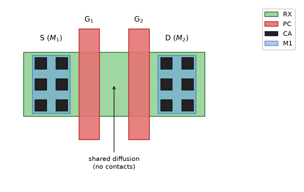
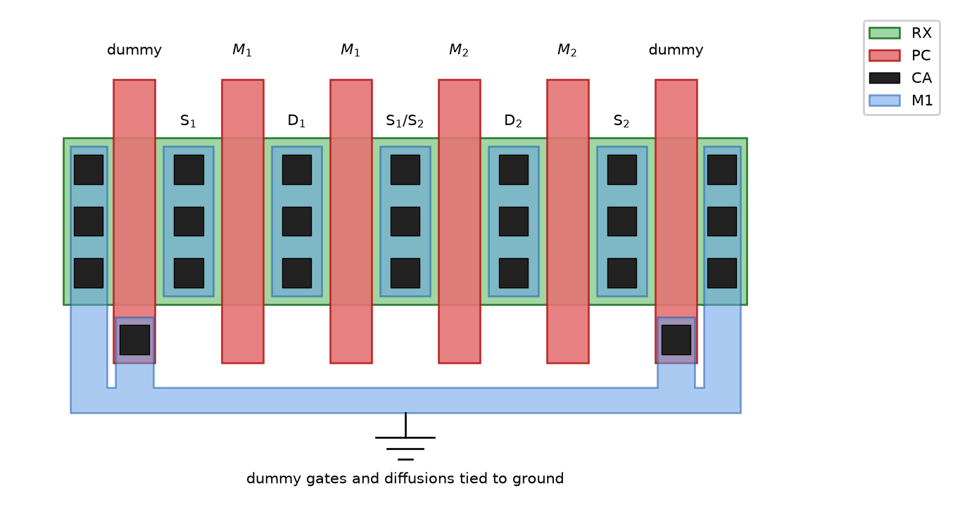
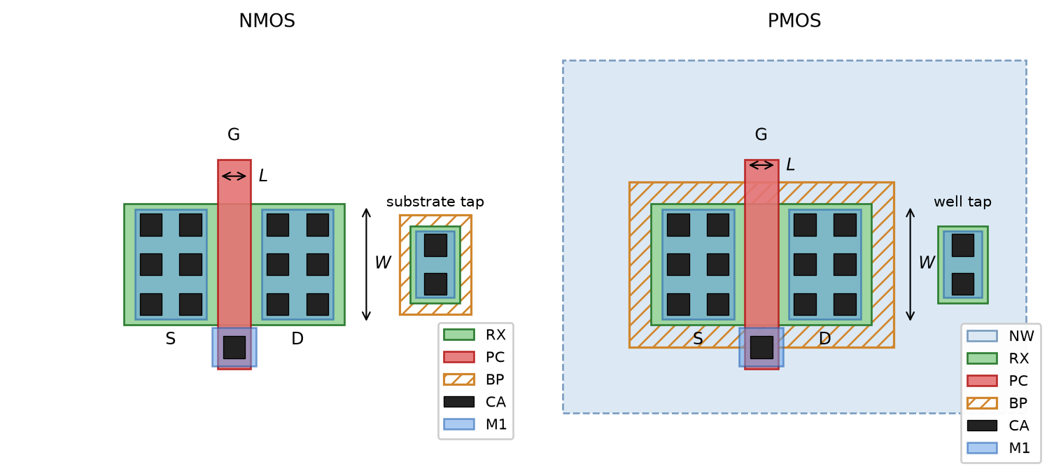
RX and PC; this intersection defines \(W\) and \(L\) of the transistor. The areas of RX not covered by PC become the source and drain regions.RX shape is contained inside a BP region (RX plus BP is \(p^+\), RX without BP is \(n^+\)).RX covered by BP (outside the n-well).RX located inside NW.NW must surround the PMOS with sufficient margin.BP is a pure marking layer, assisting mask generation and device extraction from the layout.CA contacts connect source/drain/gate as well as the \(p^+\)/\(n^+\) contacts to M1.\[ R = \rho \frac{L}{t \cdot W} = R_\square \frac{L}{W} \tag{48}\]
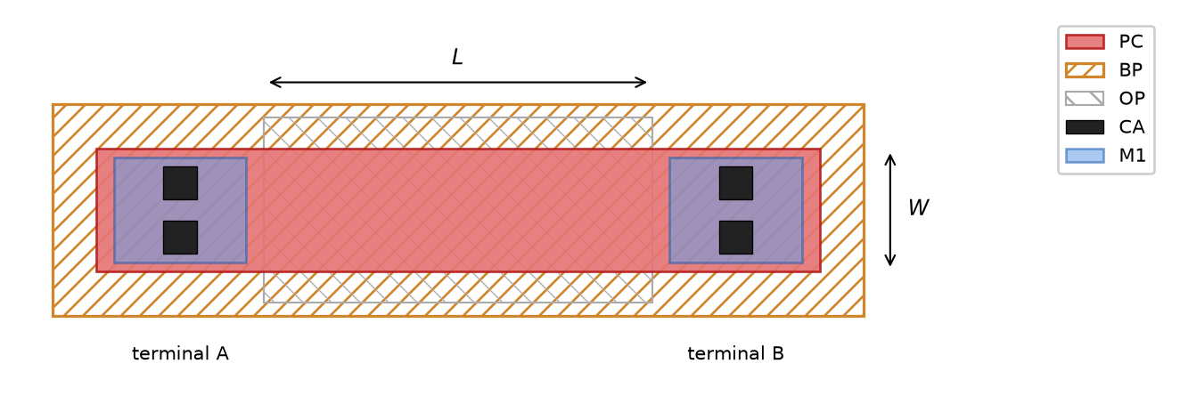
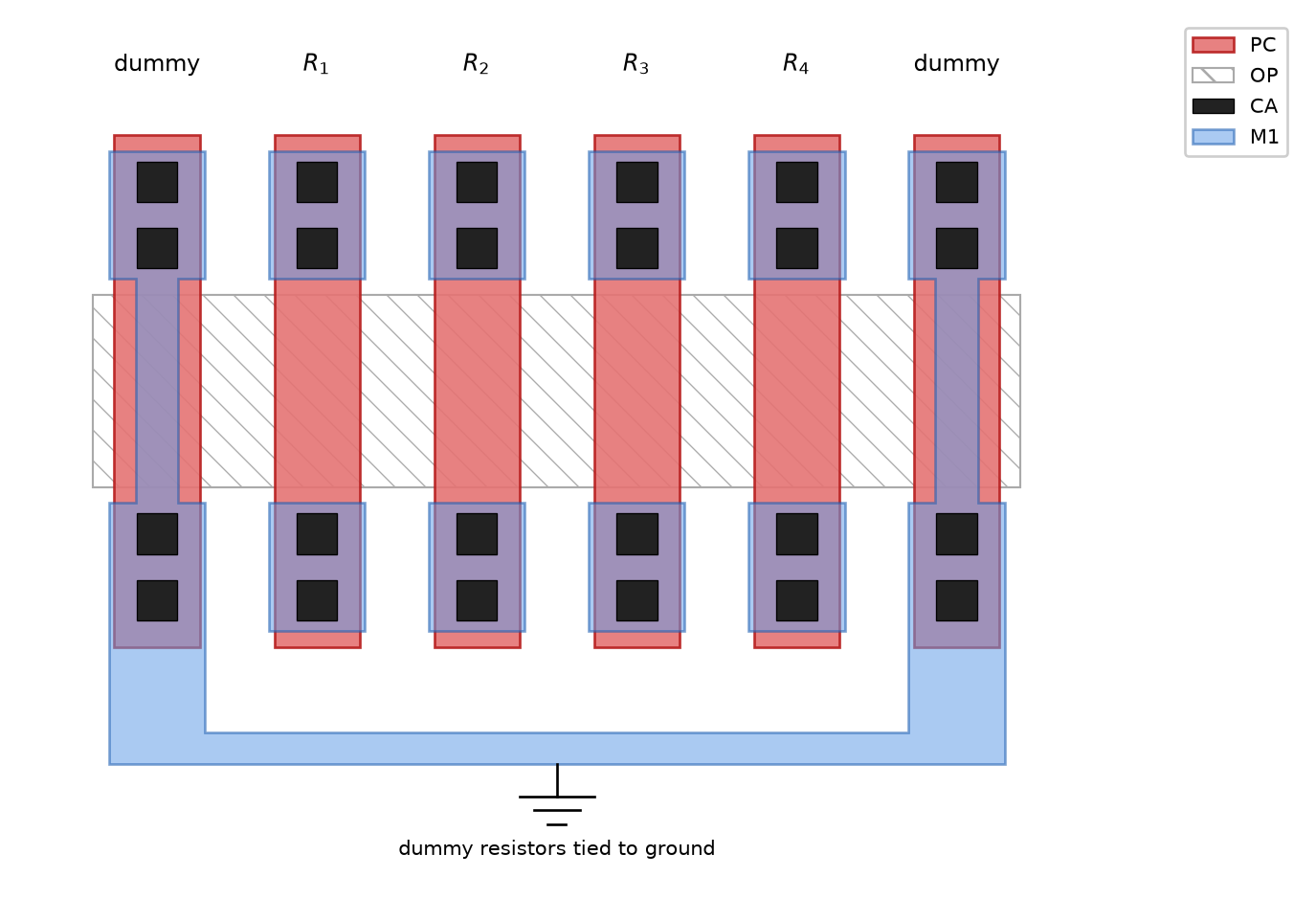
PC strip is blocked by the OP shape, whose intersection with PC defines the resistor body of length \(L\) and width \(W\); the BP marker selects \(p\)-type poly.
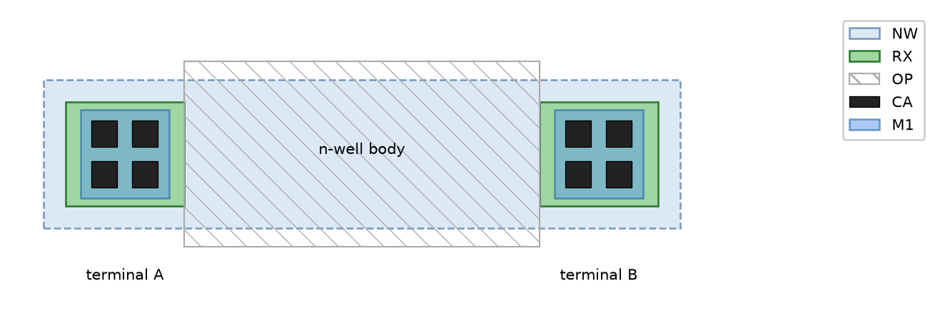
NW strip, contacted at both ends by \(n^+\) diffusions (RX); the OP shape blocks the silicide over the body.
| Type | \(R_\square\) (Ω/\(\square\)) | Process tolerance (\(\pm 4 \sigma\)) | Matching | Temp. coefficient |
|---|---|---|---|---|
Silicided \(n^{++}\)-poly (rsil) |
7 | ±12 % | 0.6 %µm | 0.3 %/K |
Blocked \(p^+\)-poly (rppd) |
260 | ±10 % | 1.5 %µm | 0.017 %/K |
Blocked compensated poly (rhigh) |
1360 | ±15 % | 4.8 %µm | −0.23 %/K |
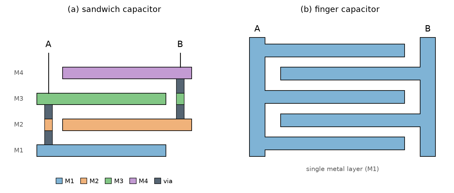
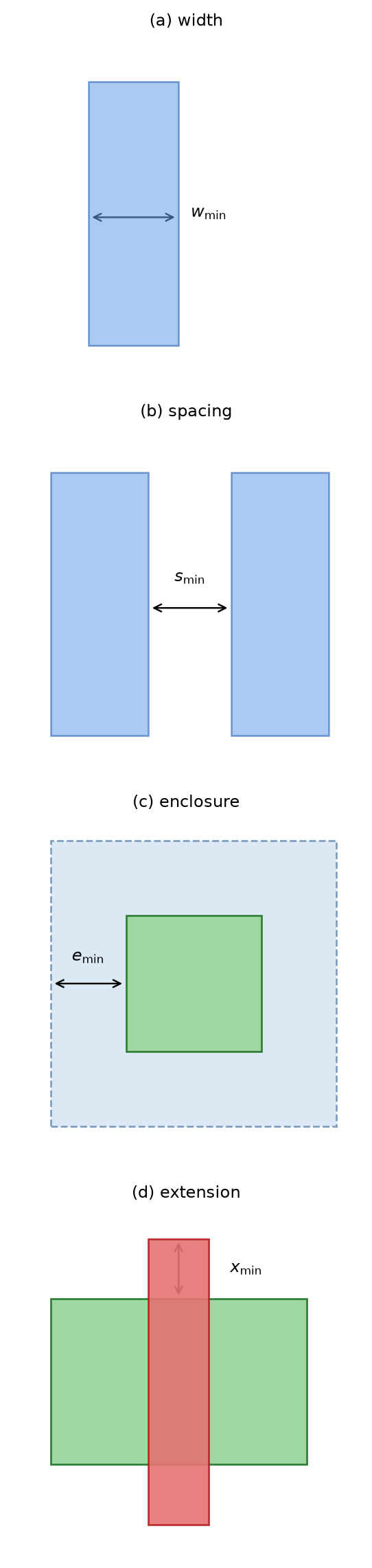
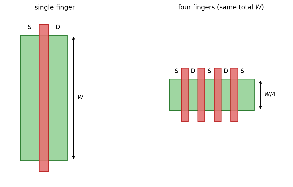
Metal5 and TopMetal1 is available (ca. 1.5 fF/µm²); the MOM finger capacitor has ca. 0.3 fF/µm², so when using 4 metal layers the effective capacitance is comparable to the MIM capacitor.RX and NW: it pays off to group PMOS and NMOS transistors together, respectively!RX in NW), and (d) minimum extension of one shape beyond another (e.g., the poly endcap over RX).
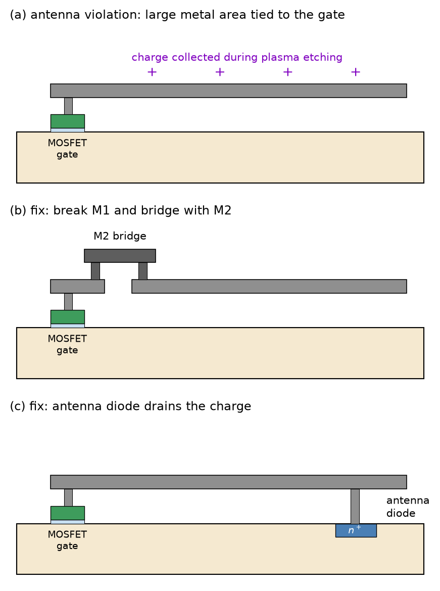
M1 wire connected to a gate collects charge during plasma etching and can destroy the gate oxide; (b) breaking the M1 wire and bridging with M2 limits the charge collected while M1 is etched; (c) an antenna diode drains the collected charge harmlessly into the substrate.
OP runs across the whole array so that every resistor body sees the same edge.
Parasitic Extraction with KLayout-PEX
Our open-source parasitic extraction tool KLayout-PEX (invoked as kpex) implements several of these extraction levels for KLayout, using different engines (an analytical 2.5D engine, a wrapper around MAGIC, and the FasterCap 3D field solver) that trade off speed against accuracy. Supported PDKs include IHP SG13G2 and SkyWater sky130A. Further information can be found in the online documentation.