Design Methodology

Design of Complex Integrated Circuits

8 Design Methodology

8.1 The Y-Diagram

The Y-Diagram

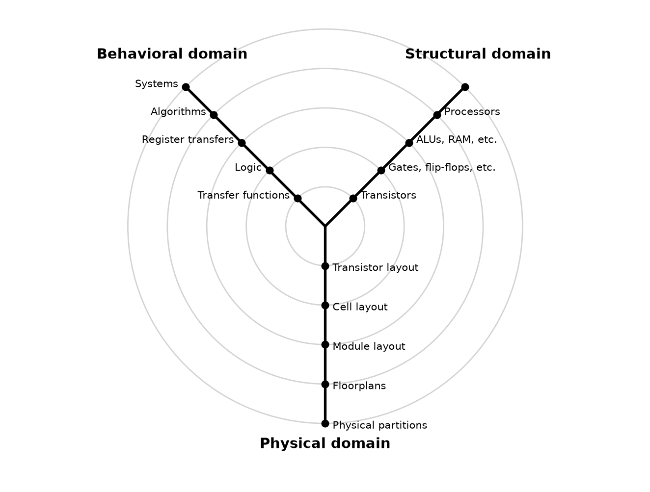
Figure 72: The Y-diagram (after Gajski-Kuhn): a design can be described in the behavioral, structural, and physical domain, on abstraction levels ranging from the system level (outer ring) to the transistor level (center).

8.2 Digital Implementation Choices

Digital Implementation Choices

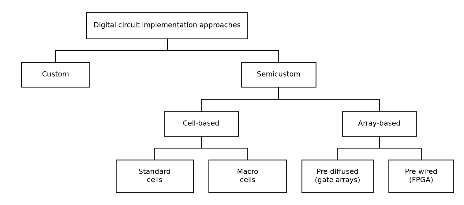
Figure 73: Taxonomy of digital circuit implementation approaches: custom design versus semicustom design, the latter split into cell-based (standard cells, macro cells) and array-based (pre-diffused gate arrays, pre-wired FPGAs) styles.

Digital Implementation Choices

  • Hard-wired logic offers the lowest power consumption, but very little flexibility.
  • Software running on a general-purpose CPU is fully flexible, but not power-efficient.
  • Software running on a domain-specific processor like a DSP or GPU sits in between.

Digital Implementation Choices

Table 13: Energy efficiency versus flexibility of digital design styles
Design style Energy efficiency Flexibility
Hardwired custom logic high low
FPGA low high
Domain-specific processor (e.g., DSP, GPU) low/mid mid
General-purpose processor (CPU) low high

8.3 Cell-Based Design

Cell-Based Design

  • A high-level description (e.g., in VHDL or SystemVerilog) can be synthesized and automatically placed and routed using standard logic cells.
  • Hard macro modules (like SRAM or IO cells) can be used to construct larger designs.
  • Soft macro modules (provided as a synthesizable high-level description or RTL) can be integrated as well.

8.3.1 Standard Cell Library

  • Logic functions (AND, OR, NAND, NOR, INV, XOR, XNOR) with 2 and more inputs (usually up to 4).
  • Complex gates (like combined AND-OR gates, half-adders, bit-shifter cells).
  • Auxiliary cells (buffers to balance delays, tie cells to bias n-wells and substrate, decoupling cells, spacers, tri-state buffers, antenna diodes).
  • Storage elements (latches, flip-flops).

Standard Cell Library

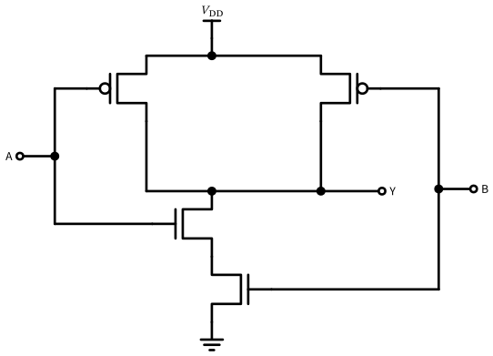
Figure 74: Transistor-level schematic of a NAND2 standard cell: two parallel PMOS pull-up transistors and two stacked NMOS pull-down transistors.

Standard Cell Library
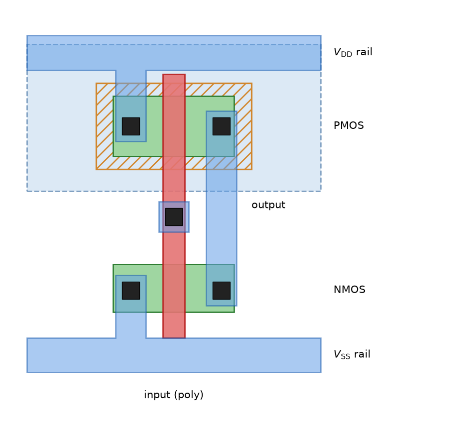
Figure 75: Typical layout organization of a standard cell (shown: an inverter): fixed cell height with horizontal \(V_\mathrm{DD}\)/\(V_\mathrm{SS}\) rails in M1 at top and bottom, the n-well with the PMOS in the upper half, the NMOS in the lower half, a shared vertical poly gate as input, and the output on M1.

8.3.2 Hard Macros

8.4 The Semicustom Design Flow

The Semicustom Design Flow

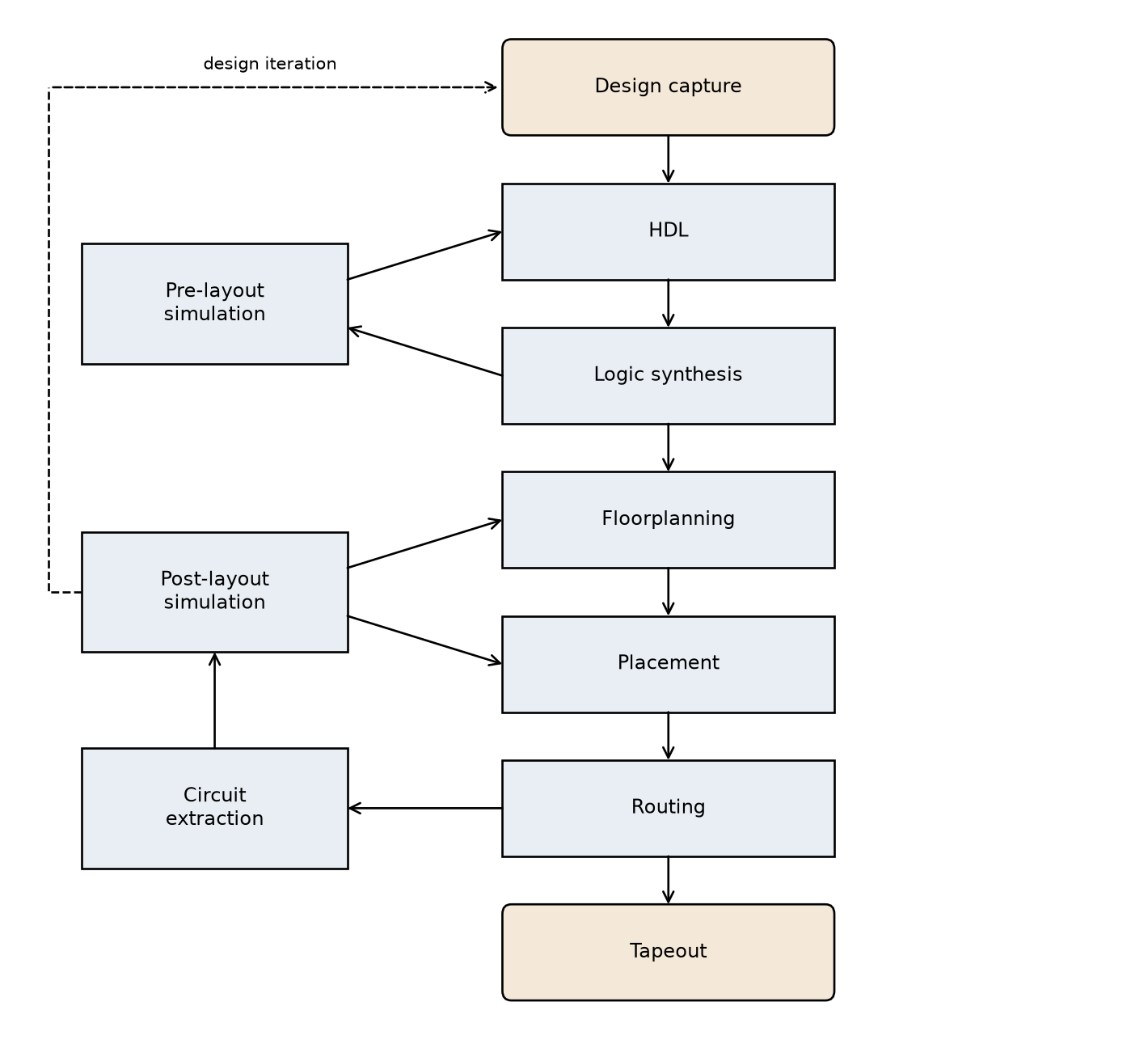
Figure 76: High-level semicustom design flow: from design capture in an HDL through logic synthesis, floorplanning, placement, and routing to tapeout.

8.4.1 RTL Synthesis

RTL Synthesis

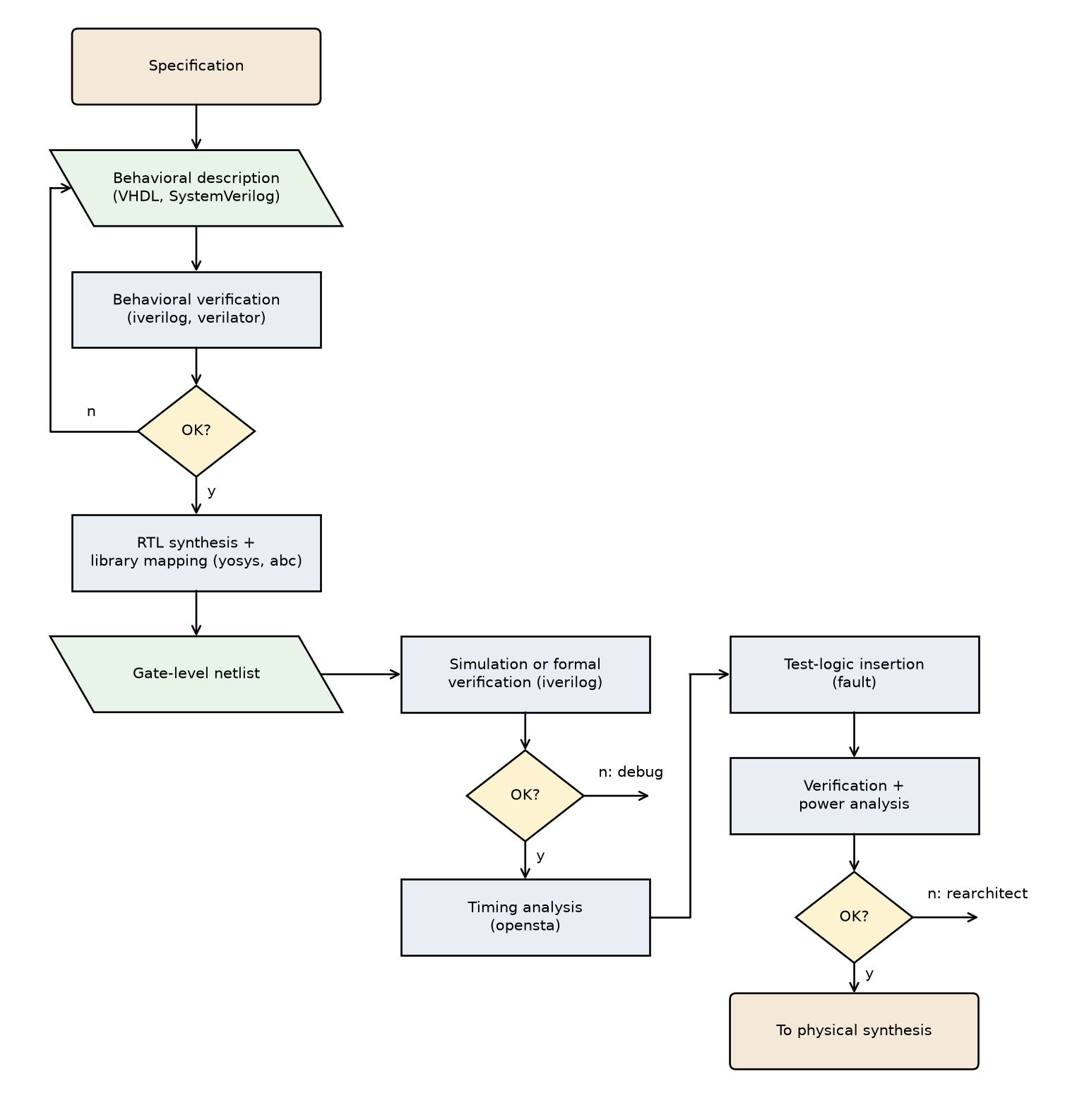
Figure 77: RTL synthesis flow with open-source tools: the behavioral description is verified by simulation, synthesized and mapped to the standard-cell library, and re-verified; static timing analysis, test-logic insertion, and power analysis complete the front-end before physical synthesis.

8.4.2 Standard-Cell Place and Route

Standard-Cell Place and Route

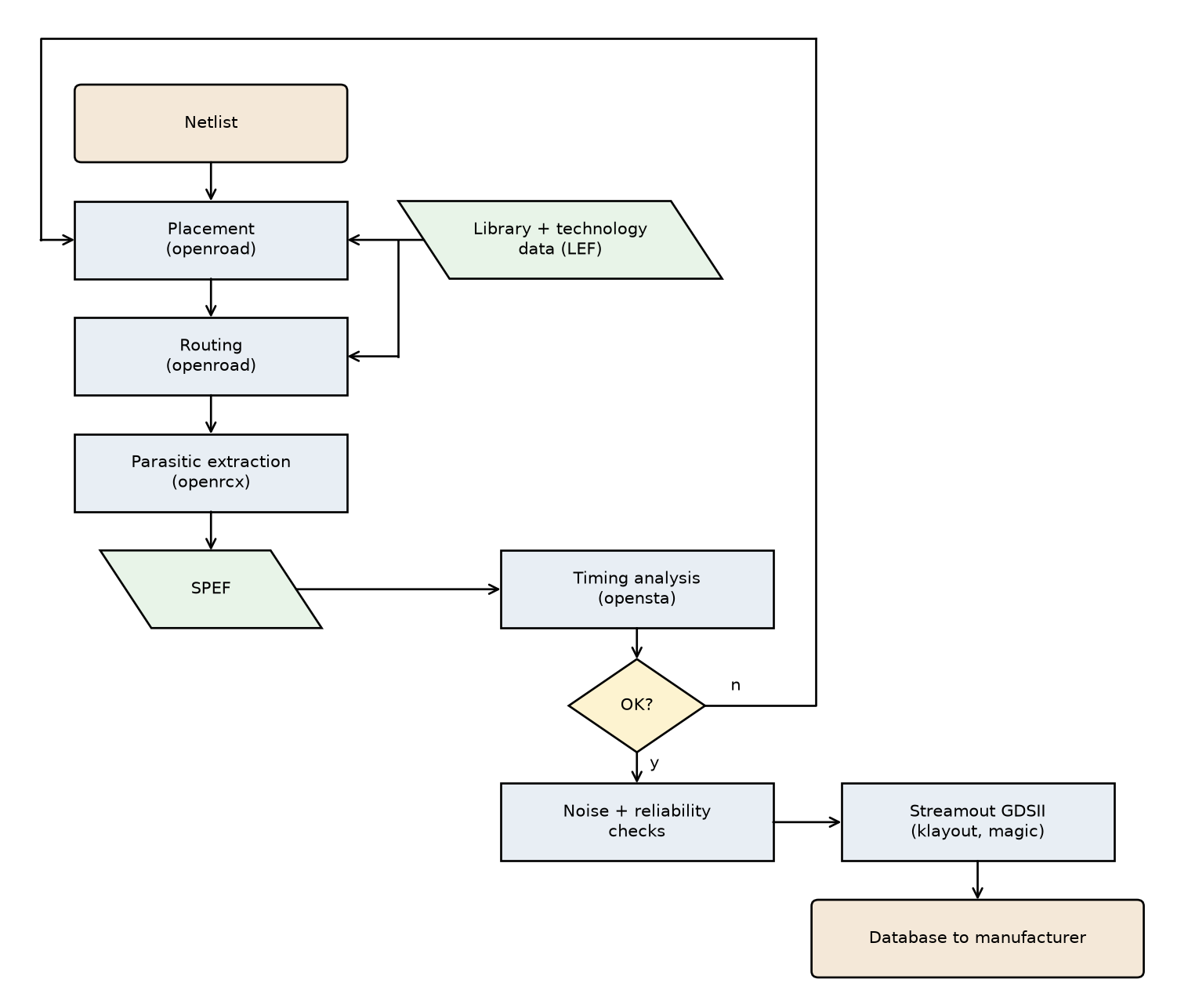
Figure 78: Standard-cell place-and-route flow with open-source tools: placement and routing (openroad) use the library and technology data (LEF); parasitic extraction (openrcx) delivers a SPEF file for post-layout timing analysis (opensta); after timing, noise, and reliability checks pass, the layout is streamed out as GDSII (klayout, magic) and sent to the manufacturer.

8.4.3 The Open-Source RTL-to-GDS Flow

8.5 The Mixed-Signal/Custom Flow

The Mixed-Signal/Custom Flow

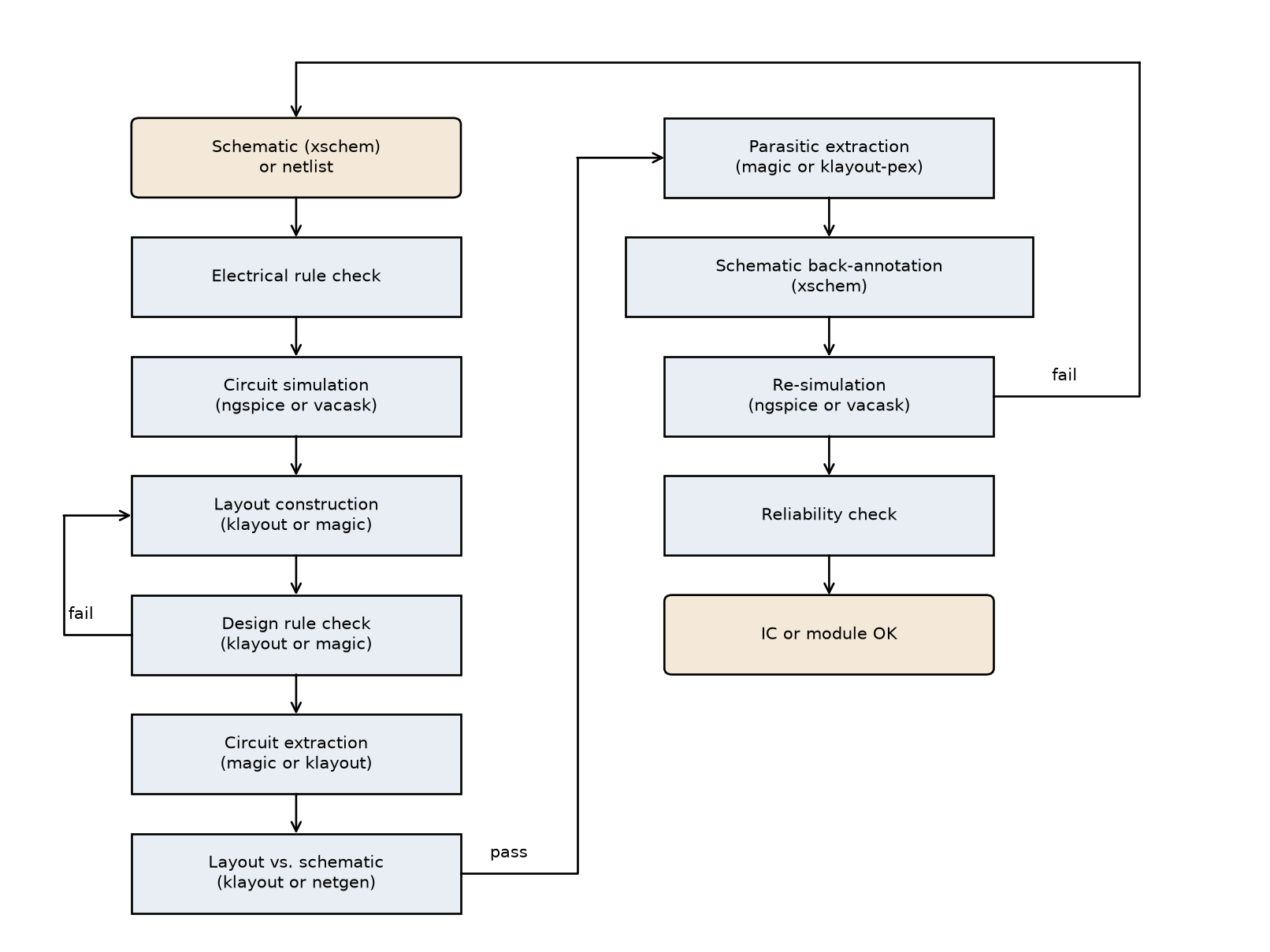
Figure 79: Mixed-signal/custom design flow with open-source tools: the schematic (xschem) is simulated (ngspice), the layout is drawn (klayout, magic) and verified by DRC, extraction, and LVS (netgen); parasitic extraction (magic) feeds a back-annotated re-simulation, and after reliability checks the block is done.

8.6 FPGAs

FPGAs

  • An FPGA consists of programmable logic blocks (typically look-up tables (LUTs) paired with flip-flops), hard macros (like CPUs, DSP slices, memory blocks, or high-speed interfaces), and a programmable interconnect fabric.
  • The flexibility is very high (the FPGA can be loaded with a new bit-stream at any time), and the performance can be high as well; however, power consumption and unit cost can be substantial.

FPGAs

  • FPGAs can also be used as (more or less) real-time test vehicles for HDL code (for prototyping and software development) before committing to a costly mask set.

References

Gajski, Daniel D., and Robert H. Kuhn. 1983. “Guest Editors’ Introduction: New VLSI Tools.” Computer 16 (12): 11–14. https://doi.org/10.1109/MC.1983.1654264.
Kahng, Andrew B., Jens Lienig, Igor L. Markov, and Jin Hu. 2022. VLSI Physical Design: From Graph Partitioning to Timing Closure. 2nd ed. Springer.
Micheli, Giovanni De. 1994. Synthesis and Optimization of Digital Circuits. McGraw-Hill.
Smith, Michael John Sebastian. 1997. Application-Specific Integrated Circuits. Addison-Wesley.
Weste, Neil H. E., and David Money Harris. 2011. CMOS VLSI Design: A Circuits and Systems Perspective. 4th ed. Addison-Wesley.

References