Electrical connection of signals and power from the IC to the PCB.
Interconnects adding little delay or distortion (small parasitic \(R\), \(L\), \(C\), and \(k\)).
Mechanical connection of the IC to the PCB.
Removal of the heat produced in the IC.
Protection of the IC from mechanical damage and the environment.
Compatibility with the thermal expansion (CTE) of the PCB.
Inexpensive manufacturing and testing.
5.2 Chip-to-Package Connection
Chip-to-Package Connection
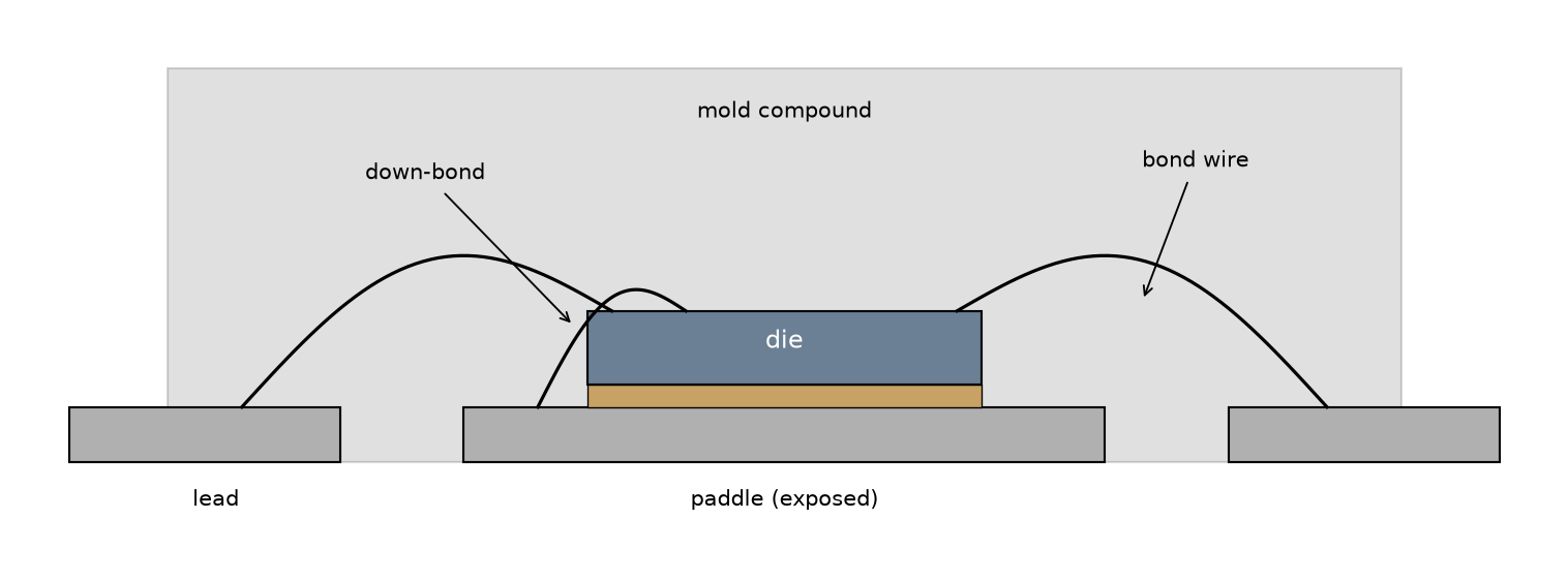
Figure 54: Cross section of a wire-bonded lead-frame package: the die is glued to the paddle, bond wires connect the die pads to the leads (a down-bond connects directly to the grounded paddle), and the epoxy mold compound protects the assembly.
Chip-to-Package Connection
A simple pad consisting only of a square of top metal may “lift off” during bonding due to insufficient adherence; a mechanically robust pad is formed from the two topmost metal layers, connected by many small vias, at the price of somewhat larger capacitance.
Pads carrying RF signals can be shaped as octagons to reduce their capacitance (about 20 % reduction).
Chip-to-Package Connection
In some processes, it is allowed to place circuitry (e.g., ESD protection) below the pads to save chip area—called pad-over-active-area (PoAA).
5.3 Package Types
Package Types
Pads can be placed across the whole surface of the die rather than only at the periphery.
The top-level metal pads are covered with solder balls.
The IC is mounted upside down and must be carefully aligned to the package (done blind!); then heat is applied to melt the solder balls.
This process is also called controlled collapse chip connection (C4).
Package Types
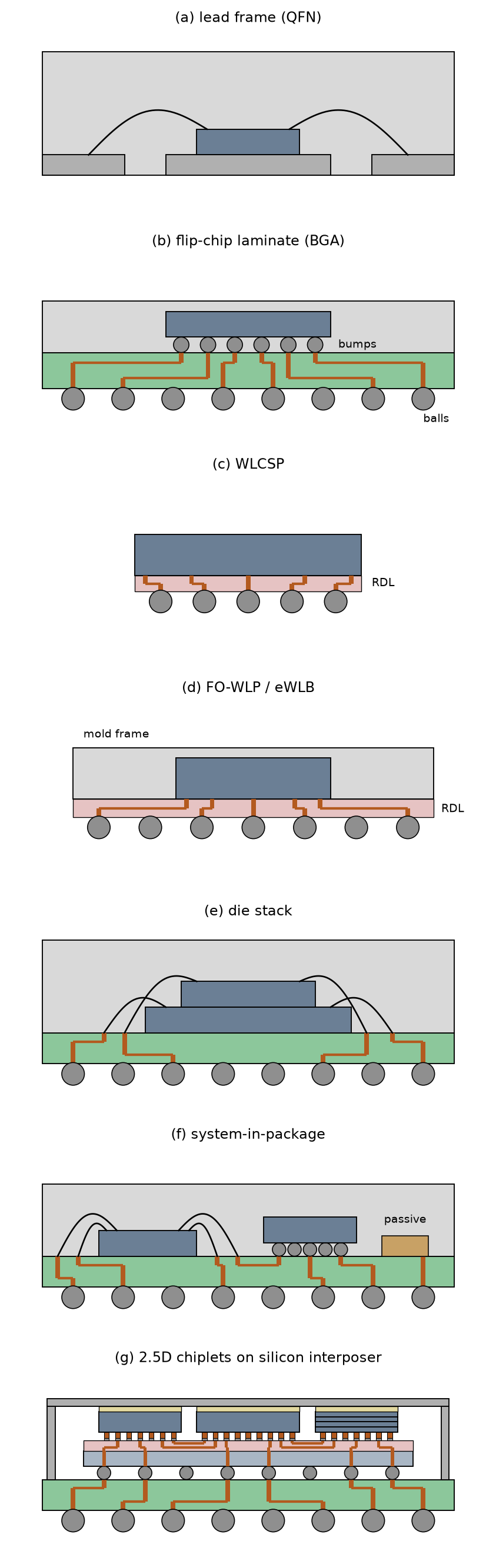
Figure 55: Cross sections of important package families: (a) wire-bonded lead-frame package (e.g., QFN), (b) flip-chip laminate package (BGA) with solder bumps and balls, (c) wafer-level chip-scale package (WLCSP), where the redistribution layer (RDL) and the balls are processed on the wafer, (d) fan-out wafer-level package (FO-WLP), where the fan-out area is created by a mold frame, (e) die stack with bond wires, and (f) system-in-package with a wire-bonded die, a flip-chip die, and a passive component on one laminate substrate, and (g) 2.5D integration, where chiplets (here two logic dice and a high-bandwidth memory stack) sit on Cu pillars on a silicon interposer with fine-pitch wiring and through-silicon vias, which is flip-chip mounted on a laminate substrate and covered by a lid.
5.3.1 Lead-Frame Package
5.3.2 Laminate Package
5.3.3 Chip-Scale and Wafer-Level Packages
5.3.4 Stacked Packages
5.3.5 2.5D Integration with Chiplets and Silicon Interposer
A single monolithic die is limited by the reticle size of the lithography tool, and the yield drops rapidly with die area; several smaller dice yield better and can exceed the reticle limit in total.
Each chiplet can be fabricated in the most suitable technology (heterogeneous integration), e.g., the compute logic in a leading-edge node, while I/O, analog, or RF functions stay in a mature, cheaper node.
2.5D Integration with Chiplets and Silicon Interposer
Memory can be placed very close to the processor; a typical example is high-bandwidth memory (HBM), a stack of DRAM dice connected by through-silicon vias.
Proven chiplets can be reused across products, reducing design effort.
5.4 Thermal Design
Thermal Design
Consumer ambient temperature range: −30 to +85 °C.
Industrial/automotive ambient temperature range: −40 to +85 °C.
Usual IC technology junction temperature limits: −40 to +125 °C.
Automotive IC junction temperature limits: −40 to +150 °C.
\[
\Delta T = R_\mathrm{th,ja} \cdot P_\mathrm{diss}
\tag{51}\]
Thermal Calculations
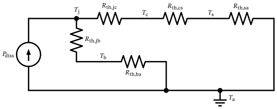
Figure 56: Thermal equivalent network of a packaged IC: the dissipated power \(P_\mathrm{diss}\) acts as a current source injecting heat into the junction node.
5.5 Package Parasitics
Package Parasitics
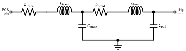
Figure 57: Equivalent circuit of a single package connection from the PCB to the on-chip pad: the bond wire and package trace contribute a series inductance and resistance, while the package trace and the bond pad add shunt capacitances.
Note 4: Example Calculation of the Bond-Wire Inductance
Let us assume a bond wire with a diameter of 25 µm (i.e., \(r = 12.5\,\mu\text{m}\)) and a length of \(l = 2\,\text{mm}\), running at a height of \(h = 300\,\mu\text{m}\) above the ground plane. With Equation 52, the inductance per length is
\[
L = L' \cdot l = 0.77\,\text{nH/mm} \cdot 2\,\text{mm} = 1.55\,\text{nH}
\]
Note that the height enters only logarithmically: doubling \(h\) to \(600\,\mu\text{m}\) increases the inductance by just 18 % to \(1.83\,\text{nH}\). At a frequency of \(f = 1\,\text{GHz}\), this bond wire already shows a reactance of
\[
X_L = 2 \pi f L = 9.7\,\Omega
\]
Package Parasitics
Example Calculation of the Bond-Wire Inductance
If this bond wire carries the supply current of a digital block, a current step of \(\Delta i = 10\,\text{mA}\) within \(\Delta t = 100\,\text{ps}\) causes a supply bounce of
\[
V = L \frac{\Delta i}{\Delta t} = 1.55\,\text{nH} \cdot \frac{10\,\text{mA}}{100\,\text{ps}} = 155\,\text{mV}
\]
which is significant for a core supply voltage of about 1.2 V.
To reduce the supply bounce, a second bond wire of the same dimensions is placed in parallel at a distance of \(d = 300\,\mu\text{m}\). With Equation 54, the mutual inductance per length is
resulting in a mutual inductance of \(L_\mathrm{m} = L_\mathrm{m}' \cdot l = 0.32\,\text{nH}\) between the two bond wires. The magnetic coupling factor is
As both bond wires carry currents in the same direction, the mutual inductance adds to the self-inductance of each wire, and the effective inductance of the parallel connection is
Instead of halving the inductance to \(0.77\,\text{nH}\), the second bond wire reduces it only by 40 %, and the supply bounce for the same current step drops from \(155\,\text{mV}\) to \(94\,\text{mV}\). A larger distance between the bond wires reduces \(k\) and brings \(L_\mathrm{eff}\) closer to \(L/2\). Conversely, if the two bond wires carry unrelated signals, the same coupling causes crosstalk: the current step of \(10\,\text{mA}\) in \(100\,\text{ps}\) in one bond wire induces a voltage of \(L_\mathrm{m} \, \Delta i / \Delta t = 32\,\text{mV}\) in the other.
5.5.1 Multiple Pads, Bond Wires, and Pins
5.5.2 Exposed Paddle and Down-Bonds
5.5.3 Mutual Inductance and Crosstalk
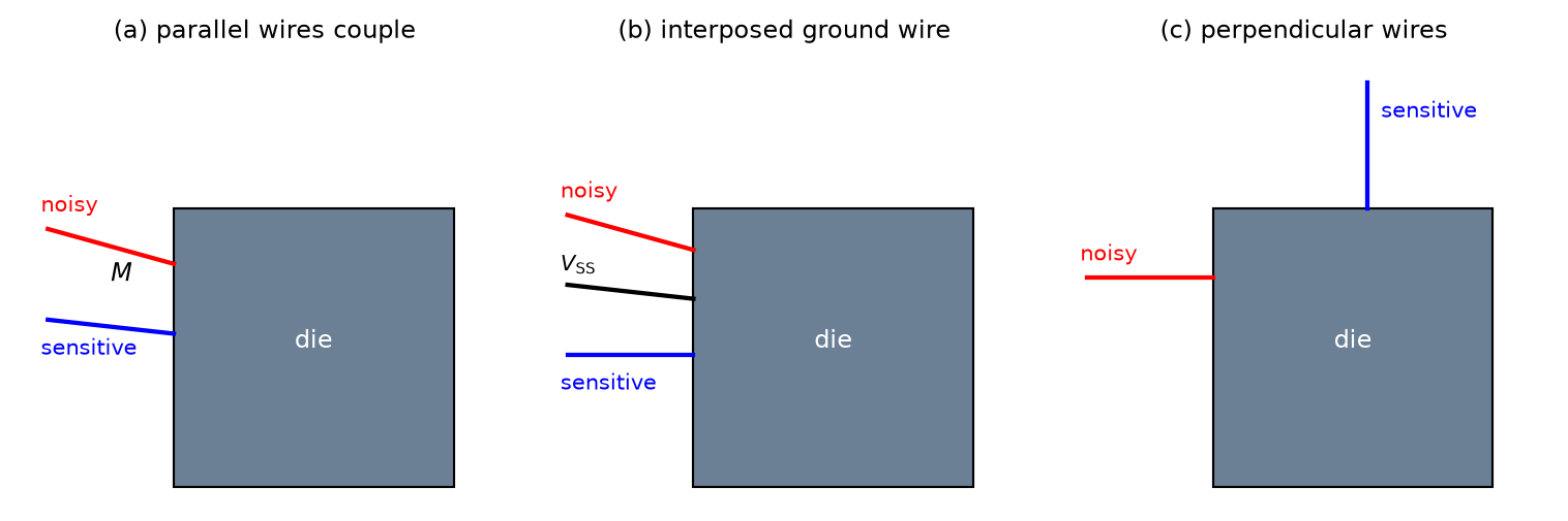
Arrange critical wires perpendicular to each other (mutual inductance requires parallel current paths).
Interpose \(V_\mathrm{SS}\) or \(V_\mathrm{DD}\) wires between critical bond wires; the return current in the interposed wire partially cancels the coupled flux.
Mutual Inductance and Crosstalk
Figure 58: Reducing mutual coupling between bond wires (top view of a chip corner): the noisy output wire couples into the parallel sensitive wire via the mutual inductance \(M\) (left); interposing a grounded \(V_\mathrm{SS}\) wire (middle) or arranging the wires perpendicular to each other at a corner (right) strongly reduces the coupling.
5.5.4 Bond Wires as Circuit Elements
5.6 Package Qualification
Package Qualification
Table 10: Typical package qualification tests
Test (examples)
Standard
Motivation & check
Pre-conditioning (PC)
JESD22-A113
Moisture soak and reflow simulate storage and board assembly before the other stress tests.
Moisture sensitivity level (MSL)
J-STD-020
Classification of how long a package may be exposed to ambient moisture before soldering.
Temperature cycling (TC)
JESD22-A104
Repeated heating and cooling must not cause failures (thermal expansion mismatch, see CTE).
Temperature humidity bias (THB) / biased HAST
JESD22-A101 / A110
Corrosion and leakage under humidity, temperature, and applied voltage.
Unbiased highly accelerated stress test (UHAST)
JESD22-A118
Exposure of package and die to high temperature and humidity without bias.
Package Qualification
Test (examples)
Standard
Motivation & check
High-temperature storage life (HTSL)
JESD22-A103
Storage at high temperature for thousands of hours (intermetallic growth).
Wire bond pull and shear
MIL-STD-883 (2011) / JESD22-B116
Mechanical strength of the bond wires and their connections.
Solder ball shear
JESD22-B117
Mechanical strength of the solder balls of BGA and WLCSP packages.
Drop test
JESD22-B111
The assembled PCB is dropped repeatedly under standardized conditions.
Temperature cycling on board (TCoB)
IPC-9701
The assembled PCB is temperature-cycled to check the solder-joint reliability.
References
Craninckx, Jan, and Michiel S. J. Steyaert. 1995. “A 1.8-GHzCMOS Low-Phase-Noise Voltage-Controlled Oscillator with Prescaler.”IEEE Journal of Solid-State Circuits 30 (12): 1474–82.
Pozar, David M. 2011. Microwave Engineering. 4th ed. Wiley.