Robust Design
Design of Complex Integrated Circuits
10 Robust Design
Robust Design
- Go for robust circuits and layouts that are insensitive to PVT (process, voltage, temperature) influences.
- Keep in mind that fabrication variations are normal; use the foundry-supplied corner models to check the design against parameter excursions and component mismatch.
- PCB, IC package, and on-chip wiring all add \(R\), \(L\), \(C\), \(k\) parasitics—model them properly and include them in the circuit simulation.
Robust Design
- During all phases of design and layout, think about what could go wrong, and build in remedies for debug and fix (layout locations where a cut or short can easily be made by FIB or a metal redesign, spare elements, programmability).
10.1 Robust Circuits and Layouts
Robust Circuits and Layouts
- Define gains by resistor ratios or capacitor ratios.
- Set currents by the ratio of a current mirror.
- Time as a parameter can be handled efficiently and accurately (crystal-referenced); if possible, base the circuit principle on timing.
Robust Circuits and Layouts
- Use negative feedback: the closed-loop gain of an amplifier is set by the feedback network (a ratio again), and is largely independent of the poorly controlled open-loop gain.
- Derive bias currents from a well-defined reference (e.g., a bandgap voltage across a resistor, or a constant-\(g_\mathrm{m}\) bias) instead of a plain supply-referenced resistor, so the circuit performance tracks with process and temperature in a controlled way.
Robust Circuits and Layouts
- Prefer differential signal paths: supply noise, substrate coupling, and even-order distortion appear as common-mode disturbances and are rejected to first order.
- Where the achievable accuracy is not sufficient, plan for calibration or trimming (see Section 6.5) instead of over-designing the circuit.
Robust Circuits and Layouts
\[ \sigma(\Delta V_\mathrm{th}) = \frac{A_{V_\mathrm{th}}}{\sqrt{W L}} \tag{65}\]
Mismatch versus Area
- Matching is best with unit elements: same size, orientation, wiring, and current-flow direction
- \(A_{V_\mathrm{th}}\) is supplied by the foundry (a few \(\text{mV}\cdot\mu\text{m}\))
- Example: \(A_{V_\mathrm{th}} = 5\,\text{mV}\cdot\mu\text{m}\), \(W L = 1\,\mu\text{m}^2\) \(\rightarrow\) \(\sigma(\Delta V_\mathrm{th}) = 5\,\text{mV}\)
- Halving the mismatch costs 4× area (and capacitance)
- Fundamental trade-off between accuracy, area, and speed
Production and Lifetime
- Anticipate the production flow:
- masks can be offset relative to each other, gradients across the wafer happen
- single defects must not cause failure (use multiple vias!)
- layout is post-processed (filling, cheesing, dummy structures)
- A working circuit has to keep working for years—wear-out mechanisms:
- electromigration in wires and vias (respect the PDK current-density limits)
- gate-oxide breakdown (TDDB)
- \(V_\mathrm{th}\) drift by HCI and NBTI/PBTI
- Keep all terminal voltages within the rated limits in all operating states (power-up, power-down, block disabled)
10.2 Corner Models
Corner Models
- Smallest/largest \(R\), smallest/largest \(C\), etc.
- Slow/fast PMOS and slow/fast NMOS, usually grouped into the corner sets SS, SF, TT, FS, FF (first letter NMOS, second letter PMOS).
Corner Models
- For digital timing, the slow corner (SS, lowest supply, highest temperature) usually limits the maximum clock frequency (setup time), whereas the fast corner (FF, highest supply, lowest temperature) is critical for hold-time violations and leakage. In advanced low-voltage nodes, temperature inversion can make low temperature the slowest condition.
- The skewed corners SF and FS are critical for circuits relying on a balance between NMOS and PMOS, such as the switching threshold of an inverter, ratioed logic, or SRAM cells.
Corner Models
- Analog circuits can have their worst case in any corner, so no corner should be skipped.
Monte-Carlo Mismatch
- Corners: fully correlated global process shift
- Monte-Carlo: random local mismatch, device parameters varied in every run
- Result is a distribution of the circuit performance (e.g., comparator offset) \(\rightarrow\) mean and \(\sigma\)
- Specs need a margin of several \(\sigma\) \(\rightarrow\) at least a few hundred runs
- Critical blocks: Monte-Carlo mismatch runs on top of the process corners
- Do not stack all worst cases at their extremes \(\rightarrow\) over-design; the spec states which conditions apply simultaneously
10.3 Include the Parasitics
Include the Parasitics
- For first investigations, hand-calculated values are a good starting point (see Section 5.5).
- For on-chip circuits, parasitic extraction (PEX) of the layout blocks is mandatory (see Section 4.8).
- For IC packages, first-order lumped models can be refined by calculated EM models (e.g., \(S\)-parameters).
- The same holds for PCB effects; if no simulation model is available, approximate the important effects by calculating \(R\), \(L\), \(C\), \(k\) from the geometry.
Supply, Ground, and Substrate
- Easily overlooked: parasitics outside the signal path
- Bond-wire inductance \(\rightarrow\) supply and ground bounce (\(L\,di/dt\))
- Resistive on-chip supply lines \(\rightarrow\) static and dynamic IR drop
- Disturbances couple into every block on the same supply, and via the resistive substrate
- Remedies: on-chip decoupling, separate supplies for noisy and sensitive blocks, parallel bond wires, guard rings
- No model available? Add a pessimistic estimate—an ideal supply and a perfect ground hide the problems seen in the lab
10.4 Failure-Mode Thinking
Failure-Mode Thinking
- If feedback-loop stability is a concern, make the compensation components (feedback \(R\) and \(C\)) programmable (using register bits and transmission gates to switch components in and out).
- If there is a critical bias point in the circuit, make it observable (connect it to a test pad via a T-gate) or programmable (adapt voltages or currents by programming, metal redesign, or FIB).
Failure-Mode Thinking
- For complex logic functions, add spare logic gates nearby (a few NAND gates, inverters, latches, and delay elements) to allow fixing overlooked logic bugs in a metal-only redesign.
- If circuit sizing is uncertain, place spare elements (\(R\), \(C\), MOSFETs, logic gates) that can be connected in a metal redesign, or by FIB for a handful of repaired samples; often, dummy elements can double in this role.
Failure-Mode Thinking
- If the risk is very high, implement multiple design variants of a circuit on one tape-out, so the best variant (based on measurements) can be selected and refined for the next tape-out.
- Route internal nodes that are hard to measure (bias voltages, reference clocks, the output of a sub-block) to an analog test bus or a test multiplexer, and provide bypass and loop-back modes, so each block of a signal chain can be characterized in isolation.
Failure-Mode Thinking
- Make sure the circuit always reaches its intended operating point: self-biased circuits like bandgap references and current references can have a second, degenerate stable state (all currents zero) and need a start-up circuit. Power-up and power-down sequences, undefined reset states, and floating inputs of disabled blocks deserve dedicated simulations.
Failure Mode and Effects Analysis
- Formalized failure-mode thinking for larger projects
- Systematically list potential failure modes
- Rank them by severity, likelihood, and detectability
- Mandatory, e.g., for automotive ICs
10.5 Debugging of ICs
Debugging of ICs
- Reproduce the failure reliably and document the conditions (sample, supply, temperature, input signals); check whether all samples fail or only some (a design issue versus a production defect).
- Isolate the failing block, e.g., using the test modes, bypass paths, and observable nodes built in during the design phase.
- Collect potential causes and form a hypothesis (the methods below help here).
Debugging of ICs
- Confirm the hypothesis by reproducing the failure in simulation, and by predicting a further observation that is then checked in the lab.
- Only then implement and verify the fix—first in simulation, then on silicon (e.g., by a FIB repair of a few samples) before the redesign is taped out.
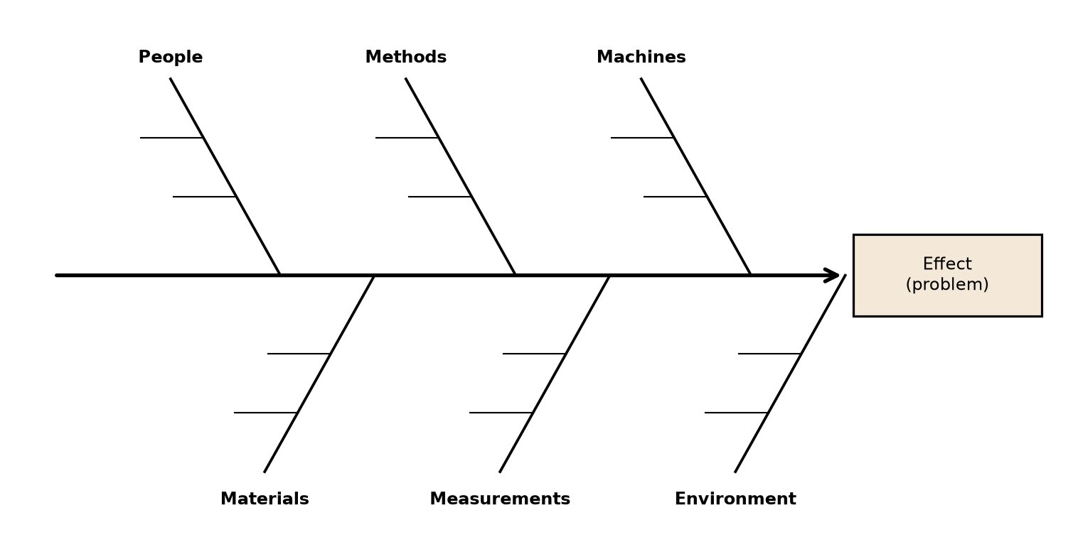
10.5.1 The Fishbone Diagram
- People: anyone involved in the process.
- Methods: policies, procedures, rules, and regulations.
- Machines: computers, tools, and equipment required to accomplish the job.
- Materials: raw materials, parts, and consumables used to produce the final product.
- Measurements: data generated from the process, used to evaluate its quality.
- Environment: the conditions—location, time, temperature, culture—in which the process operates.
The Fishbone Diagram
10.5.2 The “5-Why” Method
- “Why did the robot stop?” → The circuit overloaded, causing a fuse to blow.
- “Why did the circuit overload?” → There was insufficient lubrication on the bearings, so they locked up.
- “Why was there insufficient lubrication?” → The oil pump is not circulating enough oil.
- “Why is the pump not circulating enough oil?” → The pump intake is clogged with metal shavings.
- “Why is the intake clogged?” → Because there is no filter on the pump.
10.5.3 Focused Ion Beam (FIB)
- A FIB machine uses ions (e.g., Ga) to remove material from a sample by sputtering/milling, with a resolution down to about 10 nm.
- Using a reactive gas inside the vacuum chamber, FIB-assisted CVD can deposit structured layers of, e.g., tungsten, forming new electrical connections.
- Since the deposited layers are very thin, creating low-ohmic connections is difficult—so a cut is preferable to a new connection where possible.
Preparing for FIB
- FIB access is easiest on the top metal layers
- Route candidate nets (at least a short section) on top metal
- away from dense wiring
- not covered by metal fill
- Flip-chip or dense metal stacks: backside FIB of the thinned die possible, but considerably more difficult
10.5.4 Failure Analysis
- Micro-probing: fine needles (or FIB-created probe pads) contact internal nodes to measure voltages and waveforms directly.
- Hot-spot detection: shorts, leaky junctions, and latched structures dissipate power locally, which can be localized by thermal imaging (e.g., lock-in thermography) or by liquid-crystal coatings changing their appearance with temperature.
- Photon emission microscopy: forward-biased junctions, MOSFETs in saturation, and oxide breakdown emit weak light (mostly in the infrared), which can be detected, also through the backside of the die.
Failure Analysis
- X-ray inspection and acoustic microscopy reveal package defects like broken bond wires, voids, or delamination non-destructively; afterwards, the die can be exposed by decapsulation and inspected optically or in a scanning electron microscope (SEM).
References
Afzali-Kusha, Ali, Makoto Nagata, Nishath K. Verghese, and David J. Allstot. 2006. “Substrate Noise Coupling in SoC Design: Modeling, Avoidance, and Validation.” Proceedings of the IEEE 94 (12): 2109–38. https://doi.org/10.1109/JPROC.2006.886029.
Gandhi, Tejinder, ed. 2019. Microelectronics Failure Analysis Desk Reference. ASM International.
Giannuzzi, Lucille A., and Fred A. Stevie, eds. 2005. Introduction to Focused Ion Beams: Instrumentation, Theory, Techniques and Practice. Springer. https://doi.org/10.1007/b101190.
Hastings, Alan. 2006. The Art of Analog Layout. 2nd ed. Prentice Hall.
Ishikawa, Kaoru. 1976. Guide to Quality Control. Asian Productivity Organization.
Kinget, Peter R. 2005. “Device Mismatch and Tradeoffs in the Design of Analog Circuits.” IEEE Journal of Solid-State Circuits 40 (6): 1212–24. https://doi.org/10.1109/JSSC.2005.848021.
Ohno, Taiichi. 1988. Toyota Production System: Beyond Large-Scale Production. Productivity Press.
Pelgrom, Marcel J. M., Aad C. J. Duinmaijer, and Anton P. G. Welbers. 1989. “Matching Properties of MOS Transistors.” IEEE Journal of Solid-State Circuits 24 (5): 1433–39. https://doi.org/10.1109/JSSC.1989.572629.