Simulation of Integrated Circuits
Design of Complex Integrated Circuits
11 Simulation of Integrated Circuits
Circuit Simulators
- Verify function and performance before expensive and lengthy production
- Most circuit simulators trace back to SPICE (UC Berkeley, 1972); SPICE2 established the algorithms still in use
- Open-source digital simulators:
GHDL(VHDL),iVerilogandVerilator(Verilog/SystemVerilog) - Open-source analog/mixed-signal simulators:
ngspice,VACASK,Xyce
11.1 Formulating the Circuit Equations
Formulating the Circuit Equations
- Network \(\rightarrow\) system of equations: modified nodal analysis (MNA)
- KCL for \(N-1\) nodes, node voltages as unknowns (node 0 = ground)
- Voltage sources and inductors: branch current kept as additional unknown
- Every element adds its fixed stamp to the matrix \(\rightarrow\) very sparse matrices
Formulating the Circuit Equations
\[ i_\mathrm{R} = \frac{1}{R} ( v_1 - v_2 ), \qquad i_\mathrm{C} = C \frac{ d( v_1 - v_2 )}{dt}, \qquad \frac{di_\mathrm{L}}{dt} = \frac{1}{L} (v_1 - v_2) \]
Formulating the Circuit Equations
Note 6: MNA Example
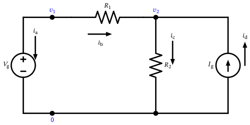
Let us perform the modified nodal analysis for the simple circuit in Figure 90. As a first step, the voltage nodes are numbered, and the directions of the branch currents are fixed. The KCL equations are formulated for each node except the reference node (current flowing out counts positive):
Node \(v_1\): \(i_\mathrm{a} + i_\mathrm{b} = 0\), and node \(v_2\): \(-i_\mathrm{b} + i_\mathrm{c} - i_\mathrm{d} = 0\).
Next, the currents are expressed through the element equations. For node \(v_1\):
\[ i_\mathrm{a} + \frac{v_1 - v_2}{R_1} = 0 \]
and for node \(v_2\), using \(i_\mathrm{d} = I_\mathrm{g}\):
\[ -\frac{v_1 - v_2}{R_1} + \frac{v_2}{R_2} - I_\mathrm{g} = 0 \]
Formulating the Circuit Equations
MNA Example
The current through the voltage source cannot be expressed by node voltages, so we keep it as an additional unknown and add the compensating equation \(v_1 - V_\mathrm{g} = 0\). Finally, everything is put into matrix form:
\[ \begin{bmatrix} \frac{1}{R_1} & -\frac{1}{R_1} & 1 \\ -\frac{1}{R_1} & \frac{1}{R_1} + \frac{1}{R_2} & 0 \\ 1 & 0 & 0 \end{bmatrix} \begin{bmatrix} v_1 \\ v_2 \\ i_\mathrm{a} \end{bmatrix} - \begin{bmatrix} 0 \\ I_\mathrm{g} \\ V_\mathrm{g} \end{bmatrix} = 0 \tag{66}\]
Formulating the Circuit Equations
MNA Example
Equation 66 has the form \(\mathbf{G} \mathbf{x} - \mathbf{w} = 0\). Since the entries of \(\mathbf{G}\) are constant in this example, the solution is simply \(\mathbf{x} = \mathbf{G}^{-1} \mathbf{w}\). Note that \(\mathbf{G}\) must be invertible (\(\det \mathbf{G} \neq 0\)), otherwise no solution can be found—and this is also true inside circuit simulators (a typical cause is a floating node without a DC path to ground, or a loop of ideal voltage sources)! Simulators never compute \(\mathbf{G}^{-1}\) explicitly but solve the system by sparse LU factorization.
Formulating the Circuit Equations
MNA Example
11.1.1 Controlled Sources
- The addition of voltage-controlled elements (VCVS, VCCS) is a straightforward extension of the MNA, as the node voltages are already part of the equation system.
- The addition of current-controlled elements (CCVS, CCCS) requires sensing a branch current; conceptually, this is achieved by inserting a 0 V voltage source, which introduces an additional unknown branch current into the equation system that can then control the dependent source.
11.2 DC Simulation
DC Simulation
\[ \mathbf{G} \mathbf{x} + \mathbf{p}(\mathbf{x}) - \mathbf{w} = 0 \tag{67}\]
11.2.1 Solving Nonlinear Equations
\[ x_{n+1} = x_n - \left[ \frac{d}{dx} f(x_n) \right]^{-1} f(x_n) \]
\[ \mathbf{x}_{n+1} = \mathbf{x}_n - \left[ \mathbf{J}(\mathbf{x}_n) \right]^{-1} \mathbf{F}(\mathbf{x}_n) \tag{68}\]
Companion Models
- Each iteration linearizes every nonlinear element at the present estimate
- Companion model: conductance (the derivative) plus current source
- Solve the resulting linear MNA system, repeat until converged
- Close to the solution: quadratic convergence
- Far from it: overshoot or divergence \(\rightarrow\) voltage change per iteration is limited (e.g., across \(pn\) junctions)
11.2.2 Convergence
RELTOL: relative tolerance of voltages and currents from one iteration to the next; default 0.001 (0.1 %).VNTOL: absolute node-voltage tolerance; default 1 µV.ABSTOL: absolute branch-current tolerance; default 1 pA.
Convergence
- The starting point of the Newton-Raphson iteration matters, so provide initial guesses for critical nodes using the
.nodesetstatement (in contrast to.ic, which forces an initial condition for the transient simulation). - Floating small resistances are critical for convergence and should be avoided; for probing currents, a 0 V voltage source is a better choice than a small resistor.
Convergence
- Very-high-impedance nodes and strong nonlinearities (e.g., in diodes) may cause convergence issues. The simulator automatically places a conductance in parallel with such structures, controlled by the parameter
GMIN(default \(10^{-12}\), i.e., 1 TΩ)—which itself can cause accuracy issues, e.g., in sample-and-hold circuits.
Convergence
- Another method to achieve convergence is source stepping: slowly ramp the voltage and current sources from zero to their final values, using the result of each step as the starting point for the next (alternatively,
GMINstepping can be used).
11.3 AC Simulation
AC Simulation
\[ \left[ \mathbf{G} + j \omega \mathbf{C} \right]\mathbf{x} - \mathbf{w} = 0 \tag{69}\]
Using the AC Simulation
- dc operating point first, then circuit linearized (small-signal conductances = Jacobian entries)
- Frequency sweep \(f_\mathrm{min} \ldots f_\mathrm{max}\): one complex linear solve per frequency
- No distortion, clipping, or frequency translation!
- Stability is only shown for the selected operating point
- Loop gain: breaking the loop by hand is error-prone \(\rightarrow\) dedicated methods (e.g.,
stb(Tian et al. 2001))
11.3.1 Noise Simulation
- Noise sources added automatically: thermal (resistors), shot and flicker noise (active devices)
- Transfer function of every source to the output (all at once via the adjoint network)
- Contributions summed in power; divided by the gain \(\rightarrow\) input-referred noise
- Contribution list per device identifies the dominant noise sources
- Based on
.ac\(\rightarrow\) no nonlinear noise (mixers, oscillators, sampled circuits) - Noiseless resistor: VCCS, or local temperature of 0 K
11.4 Transient Simulation
Transient Simulation
\[ \mathbf{C} \frac{d}{dt} \mathbf{x} + \mathbf{G} \mathbf{x} + \mathbf{p}(\mathbf{x}) - \mathbf{w}(t) = 0 \tag{70}\]
11.4.1 Discrete-Time Integration Methods
| Method | Approximation |
|---|---|
Forward Euler (FE) |
\(\frac{d}{dt}v(t_k) \approx \frac{1}{\Delta T} [ v(t_{k+1}) - v(t_k) ]\) |
Backward Euler (BE) |
\(\frac{d}{dt}v(t_{k+1}) \approx \frac{1}{\Delta T} [ v(t_{k+1}) - v(t_k) ]\) |
Trapezoidal rule (TR) |
\(\frac{d}{dt}v(t_{k+1}) \approx \frac{2}{\Delta T} [ v(t_{k+1}) - v(t_k) ] - \frac{d}{dt}v(t_{k})\) |
2nd-order backward difference (Gear2) |
\(\frac{d}{dt}v(t_{k+1}) \approx \frac{3}{2\Delta T} v(t_{k+1}) - \frac{2}{\Delta T} v(t_k) + \frac{1}{2\Delta T} v(t_{k-1})\) |
Time-Step Control
- At every time point: nonlinear system solved by Newton-Raphson (previous solution as starting guess)
- Time step adapted dynamically, trading accuracy against simulation time
- Controlled by the estimated local truncation error:
- fast signal changes \(\rightarrow\) smaller step (time point rejected if the error is too large)
- smooth signals \(\rightarrow\) larger step
- Newton-Raphson fails to converge \(\rightarrow\) step reduced
- Repeated failure \(\rightarrow\) “timestep too small” error
Discrete-Time Integration Methods
FEis an explicit method and is numerically unstable for stiff circuits (with widely separated time constants, which is the normal case), unless the time step is tiny; therefore, it is not used in general-purpose circuit simulators.TRandGear2are the most heavily used integration methods in circuit simulation.- For a fixed time step, the most accurate method is
TR, followed byGear2. TRis overly sensitive to errors of previous time steps, so do not use it with a looseRELTOL!
Discrete-Time Integration Methods
- For abrupt signal changes,
BEandTRadapt quickly, but beware of the artificial ringing introduced byTR. Gear2is efficient when simulating with tight tolerances or smooth waveforms.BE,TR, andGear2are stable on stiff circuits, butBEshows strong artificial numerical damping (TRshows none,Gear2weak damping).
11.4.2 Using the Transient Simulation
- Since no noise is modeled in the plain transient simulation, the startup of oscillators or bi-stable circuits can be inhibited—if so, a start-up pulse or an initial condition is required!
- The transient simulation can be an effective fallback to find a dc operating point if
.opdoes not converge, by slowly ramping all dc sources from zero to their final values.
Using the Transient Simulation
- If high accuracy is needed, tighten the tolerance parameters (
RELTOL,VNTOL,ABSTOL) and limit the maximum time step (TMAX). - Nonlinearity is inherently captured in
.tran—but noise is not! - When applying an FFT to transient results, make sure that all transients have settled (use
TSTARTto delay the recording of the output). As the time points are not equidistant, the waveform is interpolated before the FFT; limitTMAXaccordingly, and use coherent sampling or a window function to avoid spectral leakage.
11.5 Advanced Simulation Modes
Advanced Simulation Modes
- In the transient noise simulation, the noise sources are modeled as random signals in the time domain and added to the circuit (in
ngspice, e.g., by usingtrnoisesources, or inVACASKby using the transient noise analysis). As the noise bandwidth is linked to the time step, such simulations are slow and require many runs or long simulation times for statistically meaningful results.
Advanced Simulation Modes
- For RF simulation, there is a large discrepancy between the baseband (low) frequencies and the high carrier frequency, which makes the standard transient simulation extremely time-consuming (a small time step is dictated by the carrier, but a long simulation time by the modulation). For these cases, special methods like harmonic balance or shooting-Newton have been developed; see (Kundert 1999) for an introduction. In the open-source domain,
XyceandVACASKoffer a harmonic-balance analysis.
Commercial RF Analyses
- Periodic steady state (time domain, one periodic excitation):
pss, withpac,pstb,pnoise,pxf,psp - Quasi-periodic steady state (multiple fundamental frequencies):
qpss, … - Harmonic balance (frequency domain, natural inclusion of \(S\)-parameters and frequency conversion):
hb,hbac,hbnoise, … - Further analyses: matching (
dcmatch,acmatch), stability (stb), pole-zero (pz), \(S\)-parameters (sp), envelope following (envlp)
11.6 Device Models
Device Models
- The SPICE level-1 model (the most basic model with a minimum number of parameters).
- The BSIM family (mainly BSIM3 and BSIM4 for planar bulk CMOS, BSIM-CMG for FinFETs), the widespread industry standard.
- The PSP model, well suited for analog/mixed-signal/RF design.
Model Distribution
- Standard models maintained by the Compact Model Coalition (CMC), distributed as Verilog-A code
- Open-source flow: Verilog-A compiled by OpenVAF, loaded by
ngspice(OSDI interface) andVACASK - Corner and Monte-Carlo model sets provided by the foundry (see Section 10.2)
11.6.1 SPICE Level-1
\[ I_\mathrm{D}= \frac{1}{2} K_\mathrm{p} \frac{W}{L - 2 L_\mathrm{D}} \left[ 2 (V_\mathrm{GS}- V_\mathrm{th}) V_\mathrm{DS}- V_\mathrm{DS}^2 \right] ( 1 + \lambda V_\mathrm{DS}) \quad \text{(triode)} \]
\[ I_\mathrm{D}= \frac{1}{2} K_\mathrm{p} \frac{W}{L - 2 L_\mathrm{D}} (V_\mathrm{GS}- V_\mathrm{th})^2 ( 1 + \lambda V_\mathrm{DS}) \quad \text{(saturation)} \]
SPICE Level-1: Limitations
- Shichman-Hodges model with \(K_\mathrm{p} = \mu C'_\mathrm{ox}\) and body effect via \(\gamma\)
- No subthreshold conduction and no short-channel effects \(\rightarrow\) not below roughly 4 µm gate length
- \(C_\mathrm{GS}\) changes abruptly between saturation and triode \(\rightarrow\) convergence difficulties
11.6.2 BSIM3 and BSIM4
- Industry standard since BSIM3v3: source-referenced, threshold-voltage-based
- Captures mobility reduction, velocity saturation, DIBL, non-uniform doping, poly depletion, geometric scaling, and extrinsic parasitics
- BSIM4 adds gate current, gate-induced drain/source leakage, and improved flicker noise
- Drawback: not symmetric around \(V_\mathrm{DS}= 0\) \(\rightarrow\) critical for analog switches
- Fixed in the charge-based successor BSIM-BULK (formerly BSIM6)
11.6.3 PSP
- Symmetric, surface-potential-based model (SP + MOS Model 11), CMC standard
- Accurate \(g_\mathrm{m}/I_\mathrm{D}\) in all operating regions and accurate distortion, also at small \(V_\mathrm{DS}\)
- Detailed noise models (induced gate noise, correlation of gate and drain noise)
- Includes non-quasi-static (NQS) effects
- Used by IHP SG13 for the core and I/O MOSFETs
11.6.4 NQS Effects
\[ R_\mathrm{G,nqs} = \frac{1}{5 g_\mathrm{m}} \tag{71}\]
11.7 Digital Simulation
Digital Simulation Basics
- Much less numerically intensive than analog simulation
- Discrete signal values:
0,1,X(unknown),Z(high impedance) - Transitions only at discrete time points, considering element and wiring delays
Digital Simulation
- Event-driven simulators (like
GHDLandiVerilog) evaluate a logic element only when one of its inputs changes, and support the full language semantics including delays andX/Zstates. After synthesis and place-and-route, a gate-level simulation with delays back-annotated from an SDF file is possible, although timing is primarily verified by static timing analysis.
Digital Simulation
- Cycle-based simulators (like
Verilator) compile the design into a C++ model that is evaluated once per clock cycle, typically with two-state (0/1) logic and without delays; this is dramatically faster and well suited for large synchronous designs and long test runs (e.g., booting software on a CPU core).
Timing Simulation
- Intermediate between analog and digital simulation
- Strongly simplified MOSFET models \(\rightarrow\) no nonlinear system solves
- Minimized matrix operations, forward-Euler integration
- Trades accuracy for speed
11.8 Mixed-Signal Simulation
Mixed-Signal Simulation
- An all-analog (transistor-level) simulation of the digital part is possible but usually too time-consuming.
- For further speed-up, some analog circuits can be replaced by behavioral descriptions (e.g., in Verilog-AMS or VHDL-AMS).
Mixed-Signal Simulation
- Digital → analog (D2A): the IE is a voltage source with optional output resistance and finite transition times; the logic
0/1levels are mapped to voltage levels. - Analog → digital (A2D): the IE is a comparator with adjustable thresholds for
0and1(andXin between).
References
Bagheri, Mehran, and Yannis Tsividis. 1985. “A Small Signal Dc-to-High-Frequency Nonquasistatic Model for the Four-Terminal MOSFET Valid in All Regions of Operation.” IEEE Transactions on Electron Devices 32 (11): 2383–91.
Cheng, Yuhua, and Chenming Hu. 1999. MOSFET Modeling & BSIM3 User’s Guide. Kluwer Academic Publishers.
Gildenblat, Gennady, Xin Li, Weimin Wu, et al. 2006. “PSP: An Advanced Surface-Potential-Based MOSFET Model for Circuit Simulation.” IEEE Transactions on Electron Devices 53 (9): 1979–93.
Ho, Chung-Wen, Albert E. Ruehli, and Pierce A. Brennan. 1975. “The Modified Nodal Approach to Network Analysis.” IEEE Transactions on Circuits and Systems 22 (6): 504–9. https://doi.org/10.1109/TCS.1975.1084079.
Kundert, Kenneth S. 1995. The Designer’s Guide to SPICE and Spectre. Kluwer Academic Publishers.
Kundert, Kenneth S. 1999. “Introduction to RF Simulation and Its Application.” IEEE Journal of Solid-State Circuits 34 (9): 1298–319.
Nagel, Laurence W. 1975. SPICE2: A Computer Program to Simulate Semiconductor Circuits. UCB/ERL M520. EECS Department, University of California, Berkeley.
Tian, Michael, V. Visvanathan, Jeffrey Hantgan, and Kenneth Kundert. 2001. “Striving for Small-Signal Stability.” IEEE Circuits and Devices Magazine 17 (1): 31–41.