Testing

Design of Complex Integrated Circuits

6 Testing

6.1 Post-Silicon Production Flow

Post-Silicon Production Flow

  1. Wafer test (optional): bad dice are inked or recorded in the automatic test equipment (ATE) to avoid wasting packages on them. The cost of packaging a bad die has to be weighed against the cost of the wafer test.
  2. Wafer dicing: the wafer is cut into separate chips, and bad chips are discarded.
  3. Packaging.
  4. Final test: ensures that no parts damaged during dicing or packaging are shipped; some parameters might only be testable on the packaged device.

Post-Silicon Production Flow

  • Prototype/characterization testing is very extensive: it looks for worst-case behavior across conditions, establishes guard bands (margins for temperature and measurement uncertainty), is statistically based across hundreds or thousands of engineering samples, and test time is not the main concern.
  • Production testing is very time-critical: the tester is expensive, so minimum test time matters; the tests are based on the worst-case conditions established during characterization, and each IC is tested individually.

6.2 Test Equipment

Test Equipment

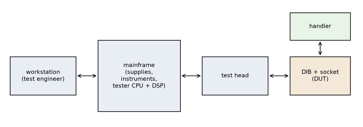
  1. The workstation: the user computer of the test engineer, used for debugging and day-to-day operation of the tester.
  2. The mainframe: houses the power supplies and measurement instruments and contains the tester computer (including DSP hardware for fast signal analysis).
  3. The test head: contains the most sensitive measurement electronics, and carries the device interface board (DIB) connecting to the device under test (DUT).

Test Equipment

Figure 59: Structure of a mixed-signal automatic test equipment (ATE): the workstation controls the mainframe (power supplies, instruments, tester computer with DSP), which connects to the test head carrying the sensitive measurement frontends and the device interface board (DIB) with the DUT socket; a handler feeds the devices.

6.3 Mixed-Signal Testing Challenges

Mixed-Signal Testing Challenges
  • Time is money: A tester plus handler can cost several million dollars, and one second of test time costs 3 to 5 cents. The test program needs a certain time (up to minutes) to cover all relevant functional blocks and critical parameters. Multi-site testing (testing 2/4/8 devices in parallel) reduces the effective test time per device.
  • The test socket introduces parasitics (\(R\), \(L\), \(C\)) which impact performance and make precision measurements difficult.

Mixed-Signal Testing Challenges

  • Accuracy is limited by interference, calibration, and measurement time.
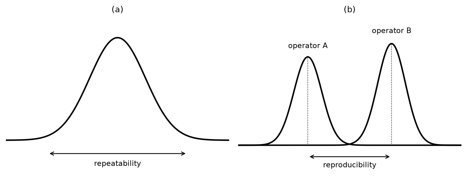
  • Repeatability & reproducibility (R&R) are required to obtain the same test results across different testers, DIBs, and test sites.

Mixed-Signal Testing Challenges

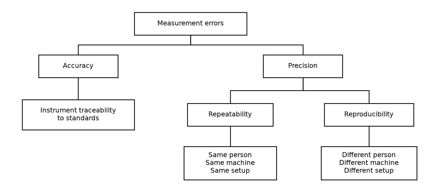
Figure 60: Classification of measurement errors: accuracy is ensured by instrument traceability to standards, while precision splits into repeatability (same person, machine, and setup) and reproducibility (different person, machine, or setup).

Mixed-Signal Testing Challenges

Figure 61: Repeatability versus reproducibility: (a) repeatability is the spread of a single measurement setup; (b) reproducibility is the difference between the mean values obtained by different operators, machines, or setups.

6.4 The Test Plan

The Test Plan

  • Device background information (in addition to the datasheet).
  • Special test requirements.
  • An explanation of the purpose of each test.
  • Assumptions made for particular tests, and why.
  • A hardware setup diagram for each test.
  • Identification of critical test parameters: not all parameters from the datasheet need to be (or can be) tested in production, due to test time or measurement error; such parameters are guaranteed by design and marked accordingly in the datasheet.

The Test Plan

  • Binning information: devices might be binned into pass/fail or different pass grades (e.g., by maximum clock frequency). Continuity fails are binned separately, because they could be caused by contact issues of the handler or socket.

6.5 Types of Tests

6.5.1 Continuity Test

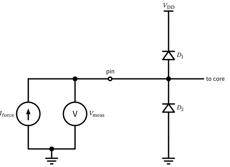
  • A high voltage (running into the voltage limit) means no contact to the IC pin → open.
  • A very small voltage means a short is detected at the IC pin → short.

Continuity Test

Figure 62: Continuity test: the tester forces a small current into the pin and measures the resulting voltage across the ESD protection diodes of the DUT.

6.5.2 Leakage-Current Test

  • A voltage is applied to all digital and analog inputs, and the current is measured.
  • Digital outputs are set to high-Z (if possible), and the leakage current is measured as for the inputs.
  • A voltage is applied to the \(V_\mathrm{DD}\) pins and the leakage current is measured; the device must be put into off-mode by applying the proper initialization (reset or power-on sequence).

6.5.3 Memory Test

  • Stuck-at faults (stuck-at-0, stuck-at-1) and transition faults (\(0 \rightarrow 1\) or \(1 \rightarrow 0\) not possible).
  • Coupling faults (writing to one cell changes the content of another cell).
  • Neighborhood pattern-sensitive faults.

Memory Test

  • Zero-one (write all zeros, read all zeros, write all ones, read all ones)—\(\mathcal{O}(n)\).
  • Checkerboard (write alternating 0101…, read, write the complement 1010…, read)—\(\mathcal{O}(n)\).
  • Walking 1/0 (consecutively fill the memory with ones/zeros and check)—\(\mathcal{O}(n^2)\).
  • ROM: read out and compute a checksum/CRC or hash—\(\mathcal{O}(n)\).

Memory Test

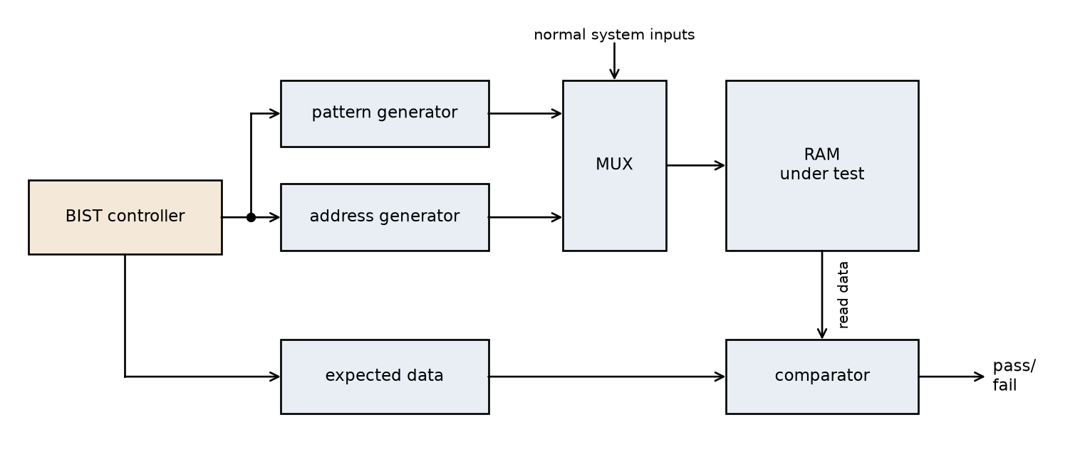
Figure 63: RAM built-in self-test (BIST): a controller sequences a test-pattern generator and an address generator that exercise the RAM through multiplexers; the read-back data is checked in a comparator, yielding a pass/fail result.

6.5.4 JTAG Test and Debug Port

JTAG Test and Debug Port

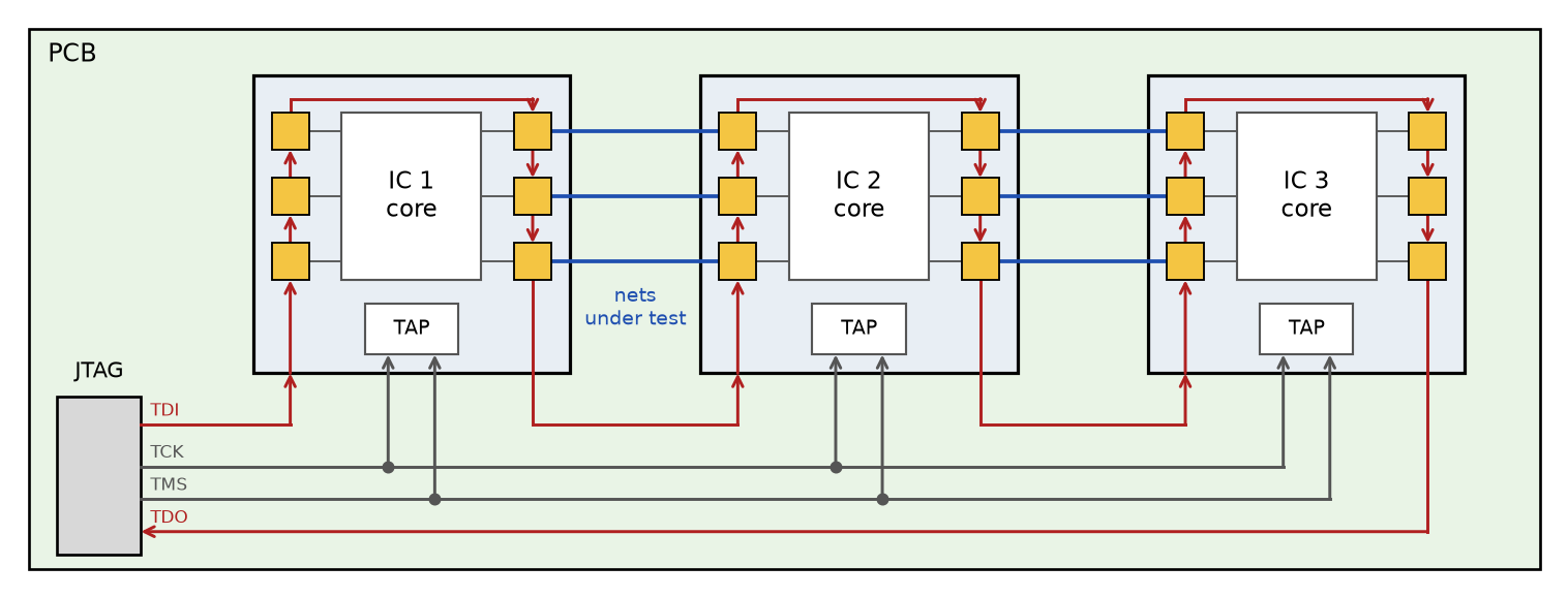
Figure 64: JTAG boundary scan on a PCB: the boundary-scan cells (small squares) at every pin of each IC form a serial shift register; the chain runs from TDI through all devices to TDO, controlled by TCK and TMS.

6.5.5 Trimming

  • If EEPROM bits are available, these can be used.
  • Fuses (e.g., polysilicon or metal wires or minimum-size vias melted open) or anti-fuses (e.g., diodes melted into a short) can permanently store a bit by forcing a high current during programming.
  • For analog precision circuits, laser trimming on the wafer can be used, e.g., to adjust the value of an integrated resistor.

6.5.6 Scan-Path Test

  • Observability: the ease of observing a node by watching the external output pins of the IC.
  • Controllability: the ease of forcing a node to 0 or 1 by driving the input pins of the IC.

Scan-Path Test

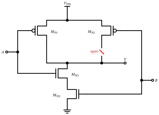
Figure 65: Limitation of the stuck-at fault model: a CMOS NAND gate with an open defect in the pull-up path of \(B\).

Scan-Path Test
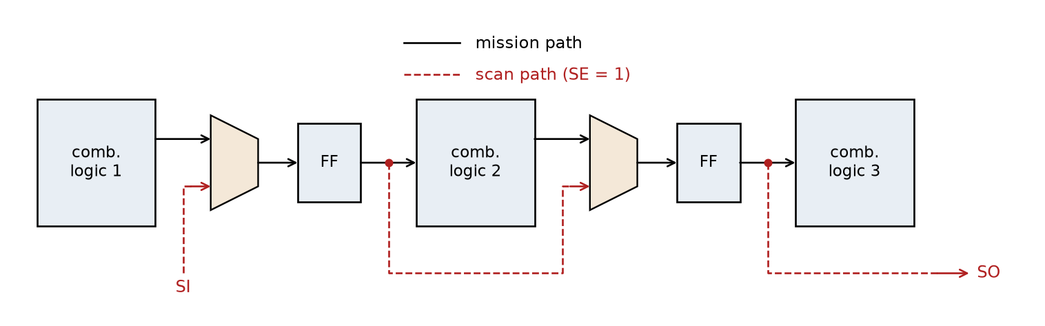
  • Each flip-flop is converted into a scan register (with a small area overhead): in mission mode, the flip-flops behave as usual; in scan mode, all flip-flops form a shift register, so their contents can be shifted in and out through dedicated pins.
  • If each register can be observed and controlled this way, the test problem reduces to testing the combinational logic between the registers.

Scan-Path Test

  • During the production test, test patterns are shifted into the scan chains, one clock cycle is applied, and the captured result is shifted out and compared to the expected result (→ pass/fail). Digital pattern generators in the ATE hardware accelerate this.
  • The patterns are generated automatically by software (ATPG) from the design netlist, achieving high stuck-at fault coverage with a minimum number of patterns.

Scan-Path Test

  • To speed up testing further, multiple chains are operated in parallel (requiring test pins for the parallel chain inputs and outputs).
  • An extension of scan is to use internal pattern generators (e.g., based on a pseudo-random number generator) as logic inputs, and to compress the outputs into a syndrome (e.g., a transition count or hash) that is compared to the expected syndrome → logic BIST.

Scan-Path Test

Figure 66: Scan-path test: every flip-flop is replaced by a scan flip-flop with an input multiplexer.

6.5.7 AC Parametric Tests

AC Parametric Tests

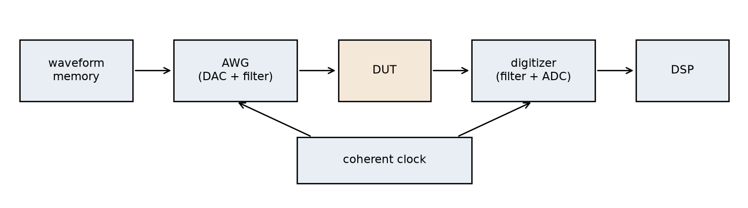
Figure 67: Mixed-signal AC parametric test setup: an arbitrary waveform generator (AWG) synthesizes the stimulus from a pattern memory, the DUT response is captured by a digitizer, and a DSP evaluates the records (FFT, filtering, averaging).

6.6 Process Capability Index

Process Capability Index

\[ \overline{X} = \frac{1}{N} \sum_{i=1}^{N} x_i \qquad \sigma = \sqrt{\frac{1}{N} \sum_{i=1}^{N} \left( x_i - \overline{X} \right)^2} \]

\[ C_\mathrm{p} = \frac{\mathrm{USL} - \mathrm{LSL}}{6 \sigma} \tag{55}\]

Process Capability Index

\[ C_\mathrm{pk} = \min \left\lbrace \frac{\mathrm{USL} - \overline{X}}{3 \sigma}, \frac{\overline{X} - \mathrm{LSL}}{3 \sigma} \right\rbrace \tag{56}\]

Process Capability Index

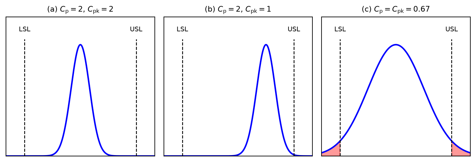
Figure 68: Process capability: (a) a well-centered distribution with small spread (\(C_\mathrm{p} = C_\mathrm{pk} = 2\)); (b) the same spread but off-center—\(C_\mathrm{p}\) is unchanged, but \(C_\mathrm{pk}\) drops to 1, indicating parts close to the upper specification limit; (c) a centered but wide distribution, where both indices are poor and yield is lost at both limits.

References

Bhunia, Swarup, and Mark Tehranipoor. 2018. Hardware Security: A Hands-on Learning Approach. Morgan Kaufmann.
Montgomery, Douglas C. 2012. Introduction to Statistical Quality Control. 7th ed. Wiley.
Wang, Laung-Terng, Cheng-Wen Wu, and Xiaoqing Wen, eds. 2006. VLSI Test Principles and Architectures: Design for Testability. Morgan Kaufmann.

References