
Fifty Nifty Variations of Two-Transistor Circuits
A tribute to the versatility of MOSFETs
ImportantThis is a web edition of a published IEEE article
The version of record is
H. Pretl and M. Eberlein, “Fifty Nifty Variations of Two-Transistor Circuits: A tribute to the versatility of MOSFETs,” IEEE Solid-State Circuits Magazine, vol. 13, no. 3, pp. 38–46, 2021, doi: 10.1109/MSSC.2021.3088968, available from IEEE Xplore.
The original paper is copyrighted by IEEE. © 2021 IEEE. Personal use of this material is permitted. Permission from IEEE must be obtained for all other uses, in any current or future media. Please cite the published version linked above.
This page reproduces the accepted author version of the text; all fifty schematics have been redrawn from scratch in Python using schemdraw, and the drawing code sits next to each figure in the repository. The two accompanying posters are archived on Zenodo under CC BY 4.0.
Abstract
We present a compendium of two-MOS-transistor circuits, spanning the range from simple standard configurations to ingenious arrangements. Using these building blocks, circuit designers can assemble a vast array of complex analog functions. This (incomplete) collection shall serve as a reference and inspiration to junior circuit designers and hopefully contains at least one unexpected example for the professional engineer.
Index terms — Basic circuits, body-driven, CMOS, MOSFET.
1 Introduction
Analog circuit design is wonderfully creative. The metal-oxide-semiconductor field-effect transistor (MOSFET) is an exceptionally versatile device, operating as a switch, a current source, a resistor, a diode, and a capacitor, depending on bias conditions. For fun and to demonstrate the sheer infinite possibilities in circuit design using MOSFETs, we present a collection of simple (and sophisticated) circuits, which employ two transistors (not counting fixed bias and supply voltages and fixed bias currents). Often, circuit designers construct complex circuits from these basic building blocks.
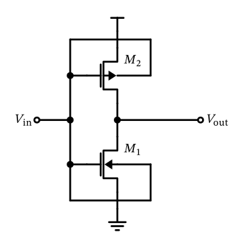
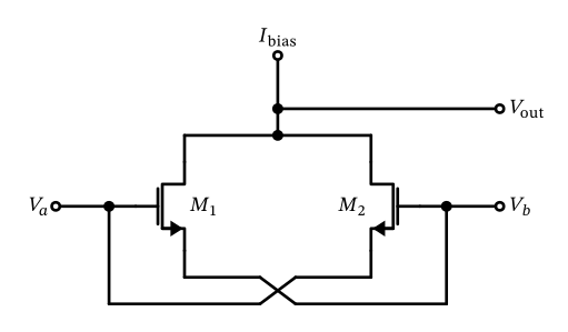
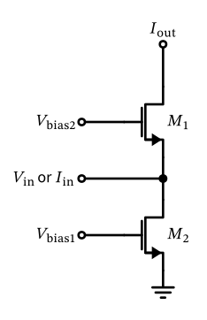
This compendium is a tribute to all the ingenious minds out there and the circuit design giants on whose shoulders we are standing today! This sample of practical two-transistor circuits, to the best of the authors’ knowledge, contains beneficial and often used configurations. A few circuits are of a more curious and academic nature, they might lack power-supply rejection or show other deficiencies, and some circuits use the body connection as active terminals (Figure 2, 16, 27, 29, 46, 49 and 50), which might not be feasible in some complementary metal-oxide-semiconductor (CMOS) technologies. Generally, one has to be aware of the body effect and its impact.
Many more two-transistor circuits are yet to be discovered. An exhaustive search of graphs using one or two voltage-controlled current sources (which are well approximated by MOSFETs) resulted in 150 potentially useful circuits (Klumperink et al. 2001), where one of them was identified as a valuable new amplifier configuration (Bruccoleri et al. 2001). By pushing this idea further, a study identified 582 possible circuit topologies using two transistors—repeating this exercise using three transistors, a whopping 56280 elementary configurations have been found (Shahhosseini et al. 2018).
To keep our overview reasonable, we do not include complementary circuits which can be constructed by swapping n-MOSFET (NMOS) for p-MOSFET (PMOS) devices (or vice versa). This can be applied to Figure 3, 4, 5, 6, 7, 8, 9, 10, 11, 12, 13, 15, 16, 17, 18, 20, 21, 22, 23, 24, 25, 26, 27, 28, 29, 30, 31, 32, 33, 34, 35, 36, 37, 38, 39, 40, 41, 42, 44, 45, 46, 47 and 48.
2 Logic Circuits
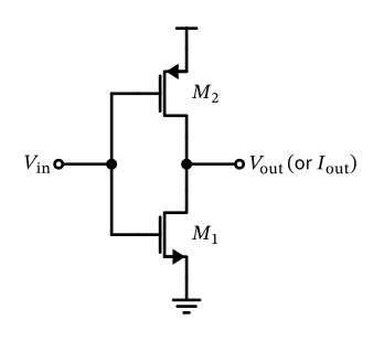
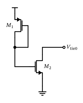
First, we present simple circuits which operate on logical inputs, like the inverter (Figure 1) and an improved low-voltage version that is exploiting the body terminals in a dynamic threshold voltage MOSFET (DTMOS) inverter (Figure 2). Terminating an unused input of a logic gate to a logical one or zero, an electrostatic discharge (ESD) safe tie-zero or tie-one, respectively, should be utilized like the one shown in Figure 3.
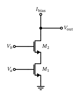
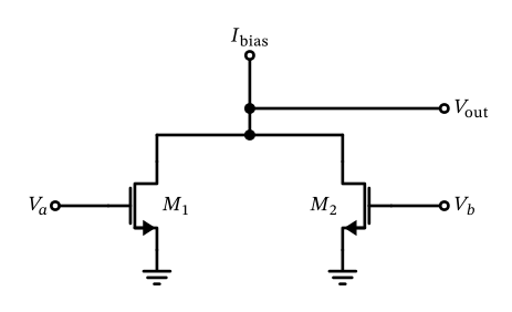
Using the unusual arrangement in Figure 4, we can implement an XNOR logic function, while the implementations of NAND and NOR, as shown in Figure 5 and Figure 6, respectively, are the fundamental building blocks of the digital universe.
3 Basic Circuits
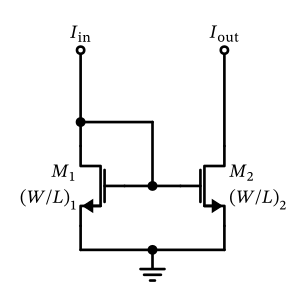
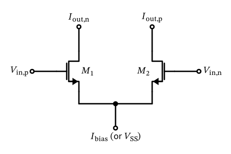
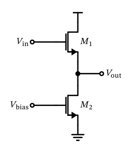
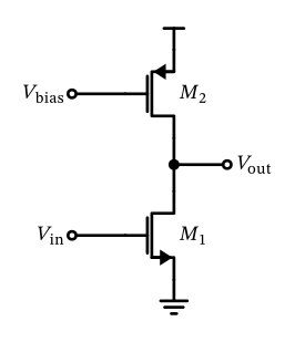
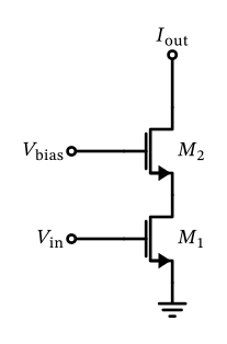
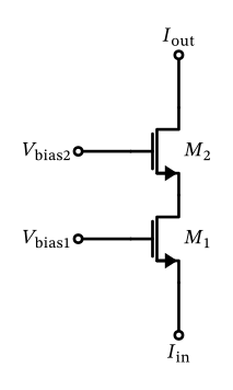
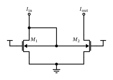
This section presents the basic circuits constituting the fundamental building blocks of the analog and mixed-signal world, like the current mirror shown in Figure 7. The differential pair (Figure 8) is alternatively constructed with or without a tail current source, often called a pseudo-differential pair. The source follower in Figure 9 is one of the elementary circuits useful in many situations, just like the common-source amplifier with active load (Figure 10). Adding a cascode to a circuit is a powerful technique. For example, a common-gate combined with a common-source stage is depicted in Figure 11, or the cascade of two common-gate stages is shown in Figure 12. Of course, the essential common-gate stage qualifies as a two-transistor circuit as well (Figure 13).
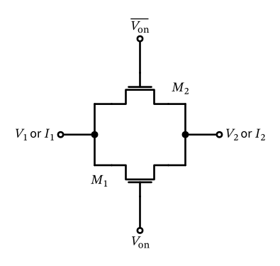
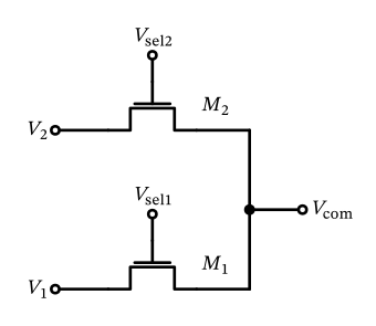
The transmission gate (Figure 14) is an essential building block, allowing switching voltages and currents (a feat making the MOSFET such a valuable device). With a straightforward extension, a multiplexer can be constructed (Figure 15). However, in most practical implementations, a set of transmission gates will be applied for this purpose.
4 Improved Basic Circuits
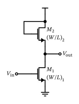
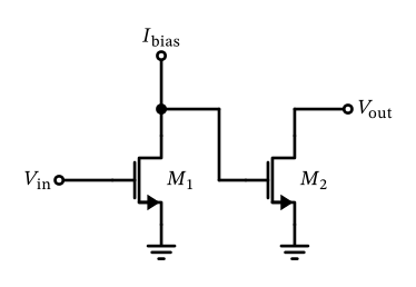
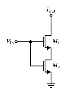
It has been realized that the digital inverter shown in Figure 1 can also be employed as an excellent low-voltage amplifier (\(V_\mathrm{out}\)) or transconductance stage (\(I_\mathrm{out}\)) when both transistors are biased in saturation. Shorting \(V_\mathrm{in}\) and \(V_\mathrm{out}\), a replica bias is readily available (Nauta and Seevinck 1989).
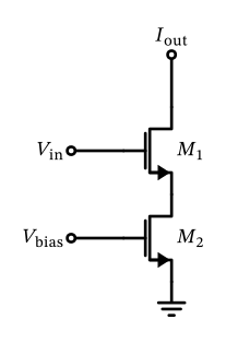
Several low-voltage circuits can be implemented using the body terminal of a MOSFET as an additional control input, like the low-voltage current mirror depicted in Figure 16. Some arrangements allow for precise voltage gain and high-speed operation, as demonstrated by the circuits shown in Figure 17 and Figure 18.
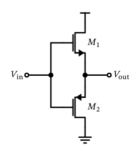
Figure 19 presents an enhanced version of the source follower, also known as class-B (push/pull) amplifier. Degeneration is a primary method to improve matching, noise figure, or output resistance. Different MOSFET-only implementations are feasible (Figure 20 and Figure 21), with the implementation in Figure 21 allowing to tune the performance during operation by varying \(V_\mathrm{bias}\).
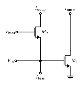
Combining a common-source stage with a common-gate topology (Nauta 1995), as shown in Figure 22, results in a differential-output transconductance stage with a single-ended low-ohmic input. It can thus be used under impedance-matched conditions, also providing some noise and linearity cancellation under ideal bias (Blaakmeer et al. 2008).
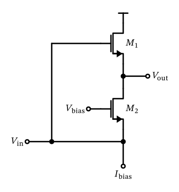
In yet another twist, a source-follower can be combined with a common-gate stage, resulting in a useful amplifier configuration (see Figure 23), which has been found by systematically generating graphs consisting of two transconductance stages (Bruccoleri et al. 2001).
5 Biasing Circuits
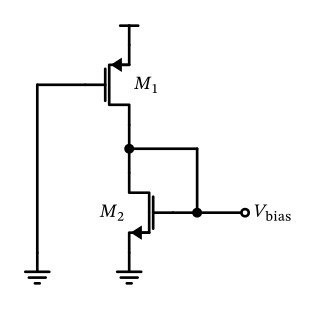
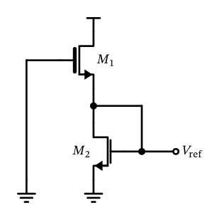
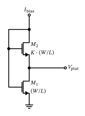
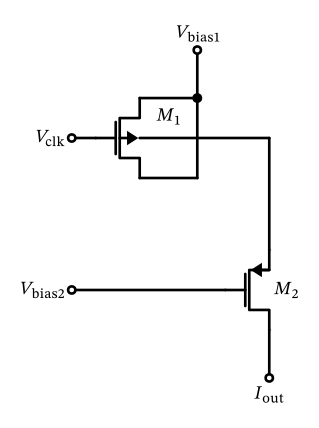
The generation of a bias voltage is a task often encountered in analog circuit design. When the requirements on stability are moderate, a simple configuration, as shown in Figure 24, might be sufficient. A surprisingly stable voltage reference can be constructed from two MOSFETs with different threshold voltages, as demonstrated in Figure 25. Occasionally, a bias voltage with a well-defined proportionality to temperature is needed, for example, in temperature sensor circuits. This effect can be achieved by a proportional-to-absolute temperature (PTAT) voltage generator like the one depicted in Figure 26. Sometimes, circuits are based on obscure second-order effects, like charge trapping in the Si–SiO\(_2\) interface traps, used in the clocked circuit shown in Figure 27, which can create pA-currents in an area-efficient manner.
6 Diverse Circuit Elements
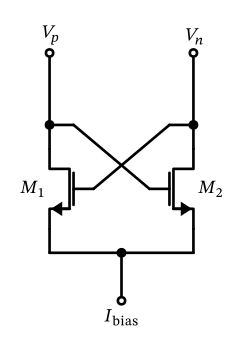
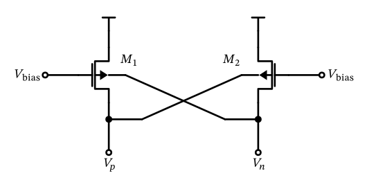
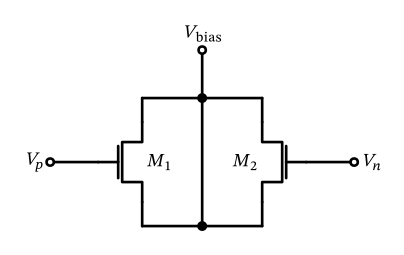
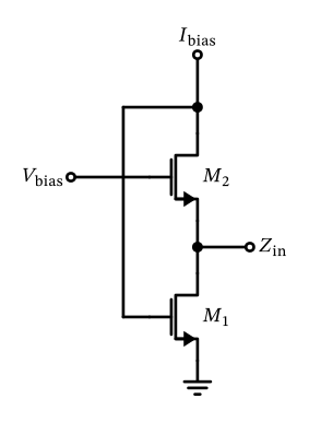
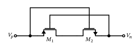
The various operating modes of a MOSFET can be utilized differently and lead to practical circuit elements. The cross-coupled differential pair (see Figure 28 and Figure 29) synthesizes a negative resistance, which can cancel losses, for example, in oscillators or \(Q\)-enhanced \(LC\) filters. Since the effective capacitance between the gate terminal and the source/drain connection of a MOSFET is a function of biasing conditions, the arrangement demonstrated in Figure 30 can be employed as a varactor.
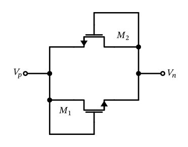
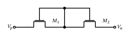
Using local feedback to create a MOSFET-“diode,” two anti-parallel diodes can replace conventional pn-diodes, for example, in voltage limiters (Figure 31). The gate oxide of a MOSFET usually offers the highest capacitance density in a given CMOS technology, so an anti-parallel pair of MOSFETs (see Figure 32) can substitute a linear capacitor with a capacitor that has mediocre linearity but is much smaller. This structure has the additional benefit of symmetric parasitic capacitors at both terminals.
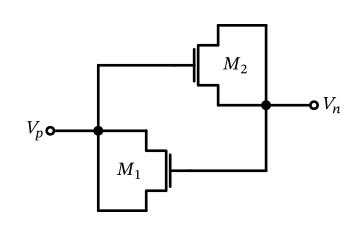
An active inductor can be simulated by transistors using gyrator principles (Qiu 1991), offering a significant area reduction compared to a passive implementation based on a coil constructed from the metal layers. An exemplary implementation based on two MOSFETs is shown in Figure 33.
7 Analog Signal Processing
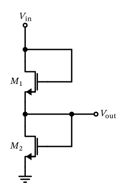
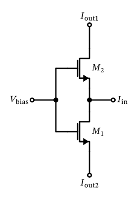
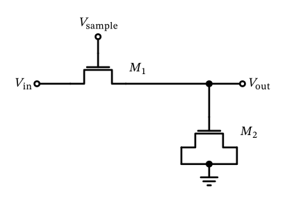
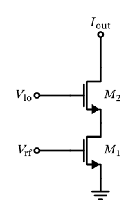
The processing of analog signals is an often needed task when devising circuits. The area-efficient division of voltages (see Figure 34) or currents (either employing a current mirror as in Figure 7 or the advanced usage of the Bult current divider, shown in Figure 35) can become handy. In any implementation of an analog-to-digital converter (ADC), a sample-hold stage is required, often exploiting the excellent switching capabilities of the MOSFET, as demonstrated in Figure 36, where a MOSFET configured as a capacitor stores the sampled voltage. Sampling can be used for frequency conversion, which can also be achieved by the arrangement in Figure 37, where the time-variant change of the transconductance of \(M_1\) causes a mixing effect (Cripps et al. 1977).
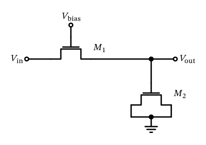
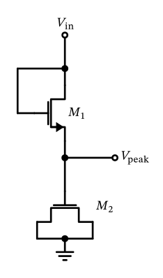
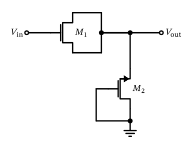
Realizing the MOSFET operating as a controlled resistor in the triode region, Figure 36 can be easily transformed into a (programmable) low-pass filter, as shown in Figure 38. By rewiring the sampling switch into the diode-equivalent MOSFET configuration, a voltage peak detector (Figure 39) and an approximate voltage doubler (Figure 40) can be built for ac signals.
8 Simple Circuits with a Twist
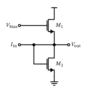
While most CMOS processes provide thin-film resistors, it is often difficult to realize values in the M\(\Omega\) to G\(\Omega\) range. The MOSFET in triode or off-state (Figure 41 and Figure 42) is a good alternative at a much smaller silicon area. An improved version of a diode-connected MOSFET is demonstrated in Figure 43. This two-transistor construction, called the ultra-low-power diode (ULPD), considerably lowers the leakage current in the reverse direction. A level-shift is often needed in a signal path, which can be implemented as pictured in Figure 44. Sometimes a simple circuit shows a surprising property, and the linear \(I\)-to-\(V\) converter shown in Figure 45 is such an example.
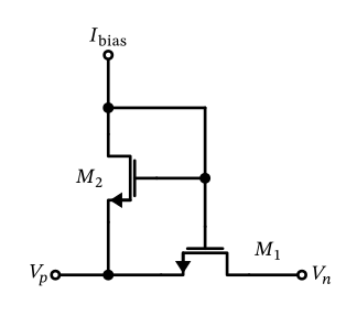
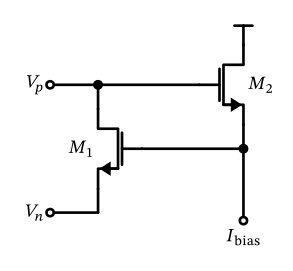
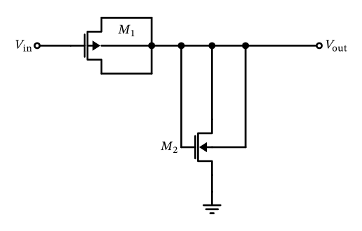
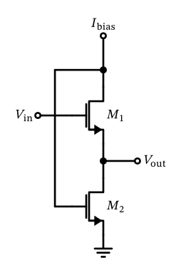
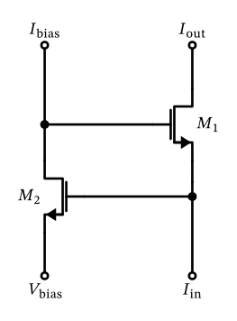
Circuits working with the body terminal as a fourth control input can add many additional possibilities, like the logic level-shift implemented in Figure 46. Feedback is an essential tool in a circuit designer’s box: the flipped voltage follower (shown in Figure 47) and the regulated cascode (see Figure 48) are significantly improved versions of their simpler counterparts shown in Figure 9 and Figure 12, respectively.
9 Using the MOSFET as a BJT
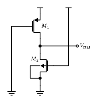
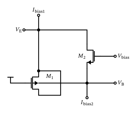
Inherent to the physical structure of a MOSFET is a bipolar junction transistor (BJT), often showing inadequate performance like poor current gain \(\beta \ll 10\). Still, it can be employed to generate a temperature-dependent voltage, like the circuit shown in Figure 49, whose complementary-to-absolute temperature (CTAT) property is an excellent addition to the PTAT behavior of the circuit in Figure 26. Compensating the low \(\beta\) of the parasitic BJT can be achieved by implementing the structure depicted in Figure 50, which improves the accuracy of a bandgap circuit built from these augmented BJT devices.
10 Conclusion
Fifty practical circuit snippets, employing just two MOS transistors, have been presented. This compilation’s motivation is to celebrate the creativity in analog circuit design and demonstrate the versatility of the fabulous MOSFET. Walking through these fifty examples—and considering that this compendium is far from complete (Shahhosseini et al. 2018)—leaves one in awe thinking about the endless possibilities when an analog circuit designer is given a handful of these fantastic transistors!
Acknowledgment
The authors thank the reviewers for their many mindful suggestions. We want to thank our colleagues at the Institute for Integrated Circuits, JKU, for their support in preparing this manuscript and many enlightening discussions!
References
Amaravati, A., M. Dave, M. S. Baghini, and D. K. Sharma. 2013. “800-nA Process-and-Voltage-Invariant 106-dB PSRR PTAT Current Reference.” IEEE Transactions on Circuits and Systems II: Express Briefs 60 (9): 577–81. https://doi.org/10.1109/TCSII.2013.2268435.
Assaderaghi, F., S. Parke, D. Sinitsky, J. Bokor, P. K. Ko, and Chenming Hu. 1994. “A Dynamic Threshold Voltage MOSFET (DTMOS) for Very Low Voltage Operation.” IEEE Electron Device Letters 15 (12): 510–12. https://doi.org/10.1109/55.338420.
Blaakmeer, Stephan C., Eric A. M. Klumperink, Domine M. W. Leenaerts, and Bram Nauta. 2008. “Wideband Balun-LNA with Simultaneous Output Balancing, Noise-Canceling and Distortion-Canceling.” IEEE Journal of Solid-State Circuits 43 (6): 1341–50.
Blalock, B. J., and P. E. Allen. 1995. “A Low-Voltage, Bulk-Driven MOSFET Current Mirror for CMOS Technology.” IEEE International Symposium on Circuits and Systems (ISCAS), 1972–75. https://doi.org/10.1109/ISCAS.1995.523807.
Blumlein, A. D. 1937. Thermionic Valve Amplifying Circuit. U.S. Patent 2,185,367.
Bruccoleri, F., E. A. M. Klumperink, and B. Nauta. 2001. “Generating All Two-MOS-Transistor Amplifiers Leads to New Wide-Band LNAs.” IEEE Journal of Solid-State Circuits 36 (7): 1032–40.
Bult, K., and G. J. G. M. Geelen. 1992. “An Inherently Linear and Compact MOST-Only Current Division Technique.” IEEE Journal of Solid-State Circuits 27 (12): 1730–35. https://doi.org/10.1109/4.173099.
Bult, K., and H. Wallinga. 1987. “A Class of Analog CMOS Circuits Based on the Square-Law Characteristic of an MOS Transistor in Saturation.” IEEE Journal of Solid-State Circuits 22 (3): 357–65. https://doi.org/10.1109/JSSC.1987.1052733.
Chatterjee, S., Y. Tsividis, and P. Kinget. 2005. “0.5-V Analog Circuit Techniques and Their Application in OTA and Filter Design.” IEEE Journal of Solid-State Circuits 40 (12): 2373–87. https://doi.org/10.1109/JSSC.2005.856280.
Cilingiroglu, U., A. Becker-Gomez, and K. T. Veeder. 2003. “An Evaluation of MOS Interface-Trap Charge Pump as an Ultralow Constant-Current Generator.” IEEE Journal of Solid-State Circuits 38 (1): 71–83. https://doi.org/10.1109/JSSC.2002.806282.
Cripps, S. C., O. Nielsen, D. Parker, and J. A. Turner. 1977. “An Experimental Evaluation of X-Band Mixers Using Dual-Gate GaAs MESFETs.” 1977 7th European Microwave Conference, 101–4.
Eberlein, Matthias. 2017. Bandgap Reference Circuit with Beta-Compensation. U.S. Patent 9,568,929 B2.
Fulkerson, D. E. 1975. “Direct-Coupled Transistor-Transistor Logic: A New High-Performance LSI Gate Family.” IEEE Journal of Solid-State Circuits 10 (2): 110–17. https://doi.org/10.1109/JSSC.1975.1050570.
Harrison, R. R. 2002. “A Low-Power, Low-Noise CMOS Amplifier for Neural Recording Applications.” IEEE International Symposium on Circuits and Systems (ISCAS). https://doi.org/10.1109/ISCAS.2002.1010674.
Hong-Yi Huang, and Jing-Fu Lin. 2002. “CMOS Bulk Input Technique.” IEEE International Symposium on Circuits and Systems (ISCAS). https://doi.org/10.1109/ISCAS.2002.1010208.
Hosticka, B. J. 1979. “Improvement of the Gain of MOS Amplifiers.” IEEE Journal of Solid-State Circuits 14 (6): 1111–14. https://doi.org/10.1109/JSSC.1979.1051324.
Klumperink, E. A. M., F. Bruccoleri, and B. Nauta. 2001. “Finding All Elementary Circuits Exploiting Transconductance.” IEEE Transactions on Circuits and Systems II: Express Briefs 48 (11): 1039–53.
Levacq, David, Christophe Liber, Vincent Dessard, and Denis Flandre. 2004. “Composite ULP Diode Fabrication, Modelling and Applications in Multi-Vth FD SOI CMOS Technology.” Solid-State Electronics 48 (6): 1017–25. https://doi.org/https://doi.org/10.1016/j.sse.2003.12.016.
Mao, R., K. Keller, and R. Ahrons. 1969. “Integrated MOS Analog Delay Line.” IEEE International Solid-State Circuits Conference (ISSCC), 164–65. https://doi.org/10.1109/ISSCC.1969.1154730.
Nauta, Bram. 1995. Single-to-Differential Converter. U.S. Patent 5,404,050.
Nauta, B., and E. Seevinck. 1989. “Linear CMOS Transconductance Element for VHF Filters.” Electronics Letters 25: 448–450(2).
Qiu, Dongming. 1991. “Circuit Design of an Integrable Simulated Inductor and Its Applications.” IEEE Transactions on Instrumentation and Measurement 40 (6): 902–7. https://doi.org/10.1109/19.119765.
Ramirez-Angulo, J., R. G. Carvajal, A. Torralba, J. Galan, A. P. Vega-Leal, and J. Tombs. 2002. “The Flipped Voltage Follower: A Useful Cell for Low-Voltage Low-Power Circuit Design.” IEEE International Symposium on Circuits and Systems (ISCAS). https://doi.org/10.1109/ISCAS.2002.1010299.
Sansen, W. 2006. Analog Design Essentials. Springer.
Seok, M., G. Kim, D. Blaauw, and D. Sylvester. 2012. “A Portable 2-Transistor Picowatt Temperature-Compensated Voltage Reference Operating at 0.5 V.” IEEE Journal of Solid-State Circuits 47 (10): 2534–45. https://doi.org/10.1109/JSSC.2012.2206683.
Shahhosseini, Delaram, Eugene Zailer, Laleh Behjat, and Leonid Belostotski. 2018. “Method of Generating Unique Elementary Circuit Topologies.” Canadian Journal of Electrical and Computer Engineering 41 (3): 118–32.
Soorapanth, T., C. P. Yue, D. K. Shaeffer, T. I. Lee, and S. S. Wong. 1998. “Analysis and Optimization of Accumulation-Mode Varactor for RF ICs.” Symposium on VLSI Circuits, 32–33. https://doi.org/10.1109/VLSIC.1998.687993.
Villard, P. 1901. “Transformateur à haut voltage. A survolteur cathodique.” Journal de Physique Théorique et Appliquée 10 (1): 28–32. https://doi.org/10.1051/jphystap:019010010002801.
Vittoz, E. A. 1983. “MOS Transistors Operated in the Lateral Bipolar Mode and Their Application in CMOS Technology.” IEEE Journal of Solid-State Circuits 18 (3): 273–79. https://doi.org/10.1109/JSSC.1983.1051939.
Wanlass, F., and C. Sah. 1963. “Nanowatt Logic Using Field-Effect Metal-Oxide Semiconductor Triodes.” IEEE International Solid-State Circuits Conference (ISSCC), 32–33. https://doi.org/10.1109/ISSCC.1963.1157450.
Widlar, R. 1965. “Some Circuit Design Techniques for Linear Integrated Circuits.” IEEE Transactions on Circuit Theory 12 (4): 586–90. https://doi.org/10.1109/TCT.1965.1082512.
Yue Wu, M. Ismail, and H. Olsson. 2000. “A Novel CMOS Fully Differential Inductorless RF Bandpass Filter.” IEEE International Symposium on Circuits and Systems (ISCAS), 149–52. https://doi.org/10.1109/ISCAS.2000.858710.
Citation
BibTeX citation:
@article{pretl2021,
  author = {Pretl, Harald and Eberlein, Matthias},
  title = {Fifty {Nifty} {Variations} of {Two-Transistor} {Circuits}},
  journal = {IEEE Solid-State Circuits Magazine},
  volume = {13},
  number = {3},
  pages = {38-46},
  date = {2021},
  url = {https://ieeexplore.ieee.org/document/9523464},
  doi = {10.1109/MSSC.2021.3088968},
  langid = {en-US}
}
For attribution, please cite this work as:
Pretl, Harald, and Matthias Eberlein. 2021. “Fifty Nifty
Variations of Two-Transistor Circuits.” IEEE Solid-State
Circuits Magazine 13 (3): 38–46. https://doi.org/10.1109/MSSC.2021.3088968.