A Tutorial on Open-Source Analog-Mixed Signal Chip Design with the ihp-sg13g2 Open-PDK

This tutorial and the underlying template repository require the IIC-OSIC-TOOLS container with tag 2026.07 or later. All commands below must be executed from within the container, and the working directory must be a folder containing the corresponding Makefile.
We happily accept pull requests to fix typos or add content! If you want to discuss something that is not clear, please open an issue!
1 Tutorial Overview
This tutorial is a step-by-step walk-through of the open-source analog-mixed signal (AMS) chip flow based on the ihp-sg13g2-ams-chip-template repository for the ihp-sg13g2 130nm Open-PDK. It covers:
- Overview and Installation of IIC-OSIC-TOOLS
- Digital macro design
- Analog macro design
- Top-level assembly and padframe generation with logos and fill structures using SystemVerilog and the LibreLane flow.
The example design used throughout the tutorial contains:
- Two digital
counter_topmacros (8-bit synchronous up-counters) - Two
inverter_topmacros, one used as a 4-channel CMOS digital inverter, one as a 2-channel analog inverter - One
RM_IHPSG13_1P_1024x32_c2_bm_bistsingle-port SRAM macro - A 32-pad padframe (8 pads per side) with I/O, power, analog, and bidirectional pads
- The top-level chip assembly with power distribution network (PDN), logos, and fill structures
The tutorial ends with a set of exercises that apply the same flow to a modified counter, a ring oscillator using the inverters, and a modified top-level floorplan and pinout. This way, all important steps of the flow are covered in a hands-on manner.
The tutorial can be used both for self-study and as the basis for a workshop. Each section can be followed independently.
After the tutorial, readers should be able to use the template repository for custom silicon projects and understand how to apply the open-source tools in the IIC-OSIC-TOOLS container to design, simulate, build, and verify AMS chips with the ihp-sg13g2 Open-PDK.
1.1 Guidelines & Cheatsheets
The following guidelines and cheatsheets should be helpful for the tutorial, the use of the template repository in general and for implementing your own custom silicon projects.
2 Tools
Numerous open-source chip design tools cover the entire development workflow for purely digital, purely analog, or mixed analog-digital chips. Managing these many tools regarding installation, updates, and maintenance is complex, especially given the rapid pace of change. Therefore, the Institute for Integrated Circuits and Quantum Computing at Johannes Kepler University (JKU) Linz, Austria decided to build an all-in-one Docker container (IIC-OSIC-TOOLS) that is updated monthly and supports all essential tools and PDKs. This eliminates the need for the time-consuming individual installation of many tools, and a reproducible development environment (important for past tapeouts) is available within a GNU/Linux-based virtual machine.
2.1 IIC-OSIC-TOOLS Overview
Figure 1 shows a rough overview of the most important tools in the IIC-OSIC-TOOLS container. Additional tools are also included, which are documented on the associated GitHub page. The open-source AMS flow used in this tutorial relies on several tools, namely Xschem, Magic, Netgen, KLayout, Ngspice, VACASK, CACE, LibreLane, Yosys, OpenROAD, Verilator, cocotb, GTKWave, and Surfer. The container also ships with four PDKs, including SkyWater sky130A, GlobalFoundries gf180mcuD, IHP ihp-sg13cmos5l and IHP ihp-sg13g2 used by this template.

2.2 IIC-OSIC-TOOLS Installation
The container runs on Linux, macOS, and Windows. The installation instructions are documented in the container’s README.md. For this tutorial, we recommend the quick one-liner installation.
Additional video walk-throughs are available for Linux and Windows.
2.3 PDK Selection
As mentioned above, the container includes four Open-PDKs. To activate or switch the active PDK, the following two options are available. More detailed instructions can be found in the container’s README.md.
.designinitfile: Copy the.designinitfile referencing the ihp-sg13g2 PDK into yourdesigns/directory and restart the container. The PDK is then picked automatically every time the container is launched in that directory.On-the-fly switch: Run
sak-pdk ihp-sg13g2
inside the container. This switches the active PDK for the current session without modifying any file. When called without arguments (sak-pdk), a list of installed PDKs is shown.
By default, the container is already configured for ihp-sg13g2, so both options above are only needed when switching between PDKs. However, since this tutorial can also be used for all other PDKs, it is worth knowing how to switch the active PDK.
3 Repository Overview
3.1 Purpose
This Makefile-driven repository simulates, builds, and fully verifies (LVS, DRC, PEX) a complete analog mixed-signal chip for the ihp-sg13g2 130nm Open-PDK, including padframe generation and top-level assembly. It uses:
- LibreLane for digital macro hardening, padframe generation and top-level assembly
- Xschem for schematic entry
- Ngspice, VACASK and CACE for analog simulation
- KLayout for viewing and routing of the layout
- Magic + Netgen and KLayout for LVS, DRC and PEX verification
- SystemVerilog, cocotb, GTKWave and Surfer for digital simulation
The repository is the starting point for your own custom silicon and provides a universal design flow solution: Just clone the repo, enter the IIC-OSIC-TOOLS container, and run make all to get a tapeout-ready analog-mixed signal chip. Focus on your design and do not care about the tools and the design flow!
Furthermore, it serves as a regression test for the above-mentioned open-source tools and their dependencies using the ihp-sg13g2 Open-PDK.
3.2 Examples
Examples based on this template are:
- TinyWhisper: An Open-Source Fully-Integrated Multi-Mode Short-Wave Transmitter for Amateur Radio Applications in 130-nm CMOS
- SPARX: An Open-Source, Automated, Programmatically Generated, Frequency-Scalable Six-Port Receiver in 130-nm CMOS
- wafer.space gf180mcuD MPW Multi-Project Chip
3.3 Directory Structure
The repository is organised into the following top-level folders. The full listing can be found in the top-level README.md.
| Folder | Purpose |
|---|---|
doc/ |
Designer documentation, including specifications, pinout, floorplan, and the PDK and tool cheatsheets. |
flow/ |
LibreLane top-level configuration with config.yaml, pdn_cfg.tcl, chip_top.sdc, plus the ArtistIC logo flow. |
ip/ |
External IP cells including bondpads, custom IO cells, and logos. |
layout/ |
Compressed GDS streams of the top-level chip, including chip_top.gds.gz and chip_top_logo_fill.gds.gz. |
LICENSES/ |
License texts referenced by the SPDX headers and REUSE.toml annotations. |
macros/ |
Recursive-style macros such as counter/ and inverter/, each with its own Makefile and README. |
netlist/ |
Synthesis, schematic, layout, and PEX netlists used for top-level LVS and simulation. |
packaging/ |
Automated bondplan generation: config, flow script, package and bondplan GDS, bonding diagrams, and bond report (see Section 7.9). |
release/ |
Tapeout submission artifacts grouped by version. |
render/ |
Chip and macro renders used in the documentation. |
rtl/ |
Top-level RTL sources, including chip_top.sv and chip_core.sv. |
schematic/ |
Xschem schematics and symbols for the top-level chip. |
scripts/ |
Helper Python and shell scripts for rendering, logo placement, and plotting. |
testbenches/ |
Xschem and cocotb testbenches for the top-level chip. |
tutorial/ |
This Quarto tutorial and its supporting materials. |
verification/ |
DRC, LVS, and signoff reports. |
3.4 Workflow
The flow is driven by Makefiles. After cloning the repository and entering the IIC-OSIC-TOOLS container, every step is invoked via a make target. The default target of every Makefile is help, so make (without arguments) prints the list of available targets. After entering the container, the starting folder is foss/designs/.
git clone https://github.com/iic-jku/ihp-sg13g2-ams-chip-template.git
cd ihp-sg13g2-ams-chip-template
make help # show available targets at the top levelInstead of git clone, you can start by clicking the green “Use this template” button on the GitHub page to create your own copy of the repository. This way, you can push your changes to your own GitHub repository and even make it public if you want to share your custom silicon design with the community.
Each macro under macros/ has its own Makefile and README.md, including macro-specific targets. These targets are invoked by the top-level build flow, but you can also run them directly from inside each macro folder. Figure 2 shows how the Makefile targets across the repository are connected.
The colour scheme groups targets by the final deliverable they produce, so beginners can follow one colour from make all to the generated outputs:
- Orange — top chip / main: This branch includes
make alland all targets that contribute to the top-level chip GDS. In thebuild-topchain of the top-level Makefile, these arelibrelane-nodrc,copy-*,add-logo-fill, andrender-gds. - Yellow — bondpad IP: This branch includes
build-bondpadand all targets insideip/sg13g2_ip__bondpad_70x70/. - Purple — logos IP: This branch includes
build-logosand the two sub-Makefiles underip/sg13g2_ip__jku/andip/sg13g2_ip__jku_names/. - Blue — digital macro: This branch includes
build-counterand themacros/counter/Makefile. - Green — analog macro: This branch includes
build-inverterand themacros/inverter/Makefile. - Red — packaging: This branch includes
bondplanand the automated bondplan flow inpackaging/(see Section 7.9). - Grey — simulation and verification: This branch includes intermediate targets that feed the coloured deliverables (
sim-all,build-all,build-macros,init-submodules,sim-*-cocotb).
Solid arrows represent direct $(MAKE) <target> calls within a single Makefile. Dashed arrows represent calls that descend into a subdirectory: recursive $(MAKE) -C <dir> all calls into a sub-Makefile (one per coloured deliverable), or the Python bondplan flow in packaging/.

make all resolves to. Every coloured branch corresponds to one deliverable (top chip, bondpad, logos, digital macro, analog macro, packaging). The grey targets connect make all to those branches.
3.4.1 Top-level targets
The top-level Makefile provides:
| Target | What it does |
|---|---|
make help |
Print the help banner and list every target with its description. |
make init-submodules |
Initialise and update git submodules (for example the ArtistIC logo flow). |
make sim-rtl-cocotb / sim-gl-cocotb |
Run the RTL / gate-level (GL) cocotb testbench for the top-level. |
make sim-gl-xschem |
Run the gate-level Xschem testbench. Converges, but it may take a long time depending on the hardware used and is therefore not included in sim-all. |
make sim-view-cocotb |
Open the latest cocotb waveform in GTKWave (or Surfer with WAVEFORM_VIEWER=surfer). |
make librelane / librelane-nodrc |
Run the LibreLane flow for the top-level (with / without DRC steps). |
make copy-reports / copy-gds / copy-netlist / copy-render |
Copy the latest LibreLane artifacts back into the source tree. |
make build-bondpad / build-logos |
Build the bondpad and the logos under ip/. |
make build-counter / build-inverter / make build-macros |
Build the digital and analog macros individually or together. |
make build-top |
Run LibreLane on the top-level, copy back all artifacts, add logos and fill structures, and render the final GDS. |
make build-all |
Init submodules, build bondpad, build logos, build macros, and build top-level. |
make klayout-verify / magic-verify |
Run LVS, DRC, and PEX for a given cell with KLayout or Magic. |
make bondplan |
Generate the bondplan (die in package, bondwires, pin table) in packaging/ (see Section 7.9). |
make all |
Full simulation, build, verification, and bondplan generation. |
make release VERSION=2.1.0 |
Copy GDS, netlists, and renders into release/v.<VERSION>/ for tapeout submission. |
See the top-level README for more details and how to use the Makefile targets.
3.4.2 Digital macro targets
The counter Makefile provides:
| Target | What it does |
|---|---|
make lint-verilog / make lint-verilog-all |
Lint a single cell or the full counter design with Verilator. |
make sim-rtl-verilog |
Run the SystemVerilog testbench with Icarus Verilog. |
make sim-rtl-cocotb / sim-gl-cocotb |
Run the cocotb RTL / gate-level simulation. |
make sim-view-verilog / sim-view-cocotb |
Open the latest waveform in GTKWave or Surfer. |
make librelane (and -nodrc, -magicdrc, …) |
Run the LibreLane flow for the counter macro. |
make generate-xspice |
Convert the gate-level netlist into an XSPICE model for Xschem. |
make sim-gl-xschem / sim-view-xschem |
Run the mixed-signal XSPICE simulation in Xschem and plot the results. |
make build-fpga |
Run the full FPGA flow: lint, synthesis, P&R, and bitstream generation. |
make build-top |
Run LibreLane, copy reports, netlists, and final views, and render the final GDS. |
make all |
Run lint, all simulations, the FPGA build, and the full macro build flow. |
See the counter README for more details and how to use the Makefile targets.
3.4.3 Analog macro targets
The inverter Makefile provides:
| Target | What it does |
|---|---|
make sim-xschem TB=<tb> / make sim-view-xschem |
Run a specific Xschem testbench and plot its results with Python. |
make sim-cace |
Run CACE Monte-Carlo / mismatch characterisations. |
make klayout-lvs / magic-lvs |
Run LVS using KLayout or Magic + Netgen. |
make klayout-drc / magic-drc |
Run DRC using KLayout or Magic. |
make klayout-pex / magic-pex (EXT_MODE=<1|2|3>) |
Run parasitic extraction in C, CC, or full-RC mode. |
make klayout-verify / magic-verify |
Run LVS + DRC + PEX for a given cell. |
make lef / make lib / make verilog |
Generate the LEF, the Liberty stub, and the Verilog stub for top-level integration. |
make build-top |
Build the analog macro deliverables: LEF, LIB, Verilog stub, GDS and rendered layout image. |
make all |
Run all simulations, the analog macro build flow and KLayout / Magic verification. |
See the inverter README for more details and how to use the Makefile targets.
4 Digital Macro Implementation
The counter macro is the digital reference macro of the template. It is a parameterisable synchronous up-counter with synchronous active-high reset implemented with SystemVerilog in counter.sv. The top-level wrapper counter_top.sv converts the chip’s active-low reset to an active-high signal. The default width is 8 bits, so the counter wraps from 255 back to 0.
4.1 Directory Structure
The counter design files are located in macros/counter/, the relevant folders are:
| Folder | Content |
|---|---|
rtl/ |
SystemVerilog sources: constants.sv, counter.sv, counter_top.sv. |
testbenches/ |
verilog/, cocotb/, and xschem/ testbenches with pre-configured GTKWave and Surfer view files. |
flow/ |
LibreLane configuration (config.yaml, pin_order.cfg, impl.sdc, signoff.sdc). |
final/ |
Final deliverables (GDS, LEF, LIB per corner, NL, PNL, SPEF, VH) copied from the latest LibreLane run for top-level integration. |
fpga/ |
Optional FPGA flow for the pico-ice board. |
netlist/ |
nl/, pnl/, spice/ and xspice/ netlists (see LibreLane cheatsheet for more details). |
schematic/ |
Xschem symbol of the macro for use in mixed-signal Xschem testbenches. |
scripts/ |
Helper scripts (XSPICE conversion, plotting, layout rendering). |
verification/ |
Yosys, antenna, STA, IR-drop, DRC, LVS, and manufacturability reports. |
render/ |
Macro renders for documentation. |
Read the counter README first to get familiar with the folder layout and the available Makefile targets. Most of the commands below are documented there as well.
4.2 Reading the RTL
The macro is split into a parameterised counter and a top-level wrapper that converts the chip’s active-low reset to the internal active-high reset of the counter.
4.2.1 counter.sv
The logic is implemented in counter.sv. It is an \(N\)-bit synchronous up-counter with reset and enable, and it wraps at CTR_MAX. \(N\) defaults to 8, so the counter counts from 0 to 255 and then wraps back to 0.
macros/counter/rtl/counter.sv
// SPDX-FileCopyrightText: 2026 Simon Dorrer and Harald Pretl
// SPDX-License-Identifier: Apache-2.0 WITH SHL-2.1
// Description: This file implements an N-bit up counter with
// synchronous reset & enable in SystemVerilog.

`default_nettype none
`ifndef __COUNTER__
`define __COUNTER__

module counter #(
  parameter int unsigned       CTR_BW  = 8,
  parameter logic [CTR_BW-1:0] CTR_MAX = 2**CTR_BW - 1
)(
  input logic               clock_i,
  input logic               reset_i,
  input logic               enable_i,

  output logic [CTR_BW-1:0] counter_value_o
);

  // Counter implementation
  always_ff @(posedge clock_i) begin
    if (reset_i) begin
      // Synchronous reset clears the counter value
      counter_value_o <= '0;
    end else if (enable_i) begin
      // Increment the counter value by 1, wrap around at CTR_MAX
      if (counter_value_o == CTR_MAX) begin
        counter_value_o <= '0;
      end else begin
        counter_value_o <= counter_value_o + 1;
      end
    end
  end

endmodule // counter

`endif
`default_nettype wire
4.2.2 counter_top.sv
counter_top.sv wraps the counter and converts the active-low reset (reset_n_i) to an active-high signal reset.
macros/counter/rtl/counter_top.sv
// SPDX-FileCopyrightText: 2026 Simon Dorrer and Harald Pretl
// SPDX-License-Identifier: Apache-2.0 WITH SHL-2.1
// Description: This file implements the top-level wrapper module
// of the counter macro in SystemVerilog.

`default_nettype none
`ifndef __COUNTER_TOP__
`define __COUNTER_TOP__

module counter_top #(
  parameter  int unsigned CTR_MAX = `COUNTER_MAX_DEFAULT,
  localparam int unsigned CTR_BW  = $clog2(CTR_MAX + 1)
)(
  input logic               clock_i,
  input logic               reset_n_i,
  input logic               enable_i,

  output logic [CTR_BW-1:0] counter_value_o
);

  // Internal active-high reset (wrapper handles polarity conversion)
  logic reset;
  assign reset = ~reset_n_i;

  // Embed Counter
  counter #(
    .CTR_BW(CTR_BW),
    .CTR_MAX(CTR_MAX)
  ) counter_0 (
    .clock_i(clock_i),
    .reset_i(reset),
    .enable_i(enable_i),
    .counter_value_o(counter_value_o)
  );
endmodule // counter_top

`endif
`default_nettype wire
Shared defaults are defined in constants.sv. For example, for the final implementation, the maximum counter value is defined in constants.sv with the variable COUNTER_MAX_DEFAULT. For the testbenches, CLK_FREQ_DEFAULT is defined there to set the default clock frequency (e.g. 50 MHz) for the simulations. They are exposed as `define macros instead of a SystemVerilog package, because Yosys 0.64 cannot parse import pkg::* in a module header.
Open the three RTL files (using gedit or vim), follow and understand the counter through reset, hold, increment, and wrap-around.
4.3 Linting
Linting is done with Verilator and can be executed with the following commands.
cd macros/counter
make lint-verilog                # lint the full counter_top design
make lint-verilog CELL=counter   # lint only the standalone counter
make lint-verilog-all            # lint counter and counter_top in sequence
make lint-verilog-all is also the lint step called by make all.
4.4 Simulation
4.4.1 RTL with SystemVerilog testbench (Icarus Verilog)
A SystemVerilog testbench (counter_top_tb.sv) checks reset, hold, increment, and wrap-around. Run it with the following commands.
make sim-rtl-verilog
make sim-view-verilog               # open in GTKWave (default)
make sim-view-verilog WAVEFORM_VIEWER=surfer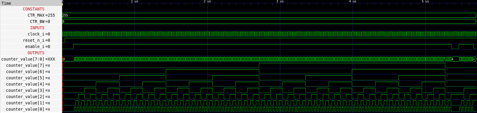
counter_top in GTKWave.
4.4.2 RTL and gate-level with cocotb
The cocotb testbench (counter_top_tb.py) checks the same four cases (reset, hold, increment, and wrap-around) as the SystemVerilog testbench, but implements them in Python.
make sim-rtl-cocotb                # RTL simulation
make sim-gl-cocotb                 # post-synthesis gate-level simulation
make sim-view-cocotb               # view in GTKWave
make sim-view-cocotb WAVEFORM_VIEWER=surfer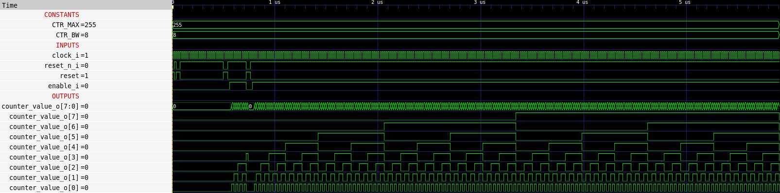
counter_top in GTKWave.
The gate-level cocotb run uses the gate-level Verilog netlist produced after synthesis: netlist/nl/counter_top.nl.v. In this tutorial, this netlist for the counter already exists. For new designs, run make build-top first to execute the LibreLane flow, then run make copy-netlist to copy the netlists from the latest LibreLane run.
4.5 LibreLane Hardening
The LibreLane flow synthesises, places, and routes the macro, runs the verification steps, and writes its final output files to flow/final/. The wrapper target make build-top runs the flow, renders the final GDS, and copies the reports, final folders, netlists, and render output back into the source tree.
make build-topThe macro can also be built as an FPGA bitstream (fpga/) for a pico-ice board (or other FPGA boards) with make build-fpga. The FPGA flow is not used in this tutorial and is only listed here for reference.
4.6 Viewing the Macro
After the flow finishes, the macro layout can be inspected with KLayout. The container provides the ke alias for klayout -e (edit mode). With the following command, the final GDS from the latest LibreLane run is opened in KLayout. With the keys 0, 1, 2, …, 9 you can view different layers as explained in the KLayout cheatsheet or in the klayout-layer-shortcuts plugin.
ke final/gds/counter_top.gds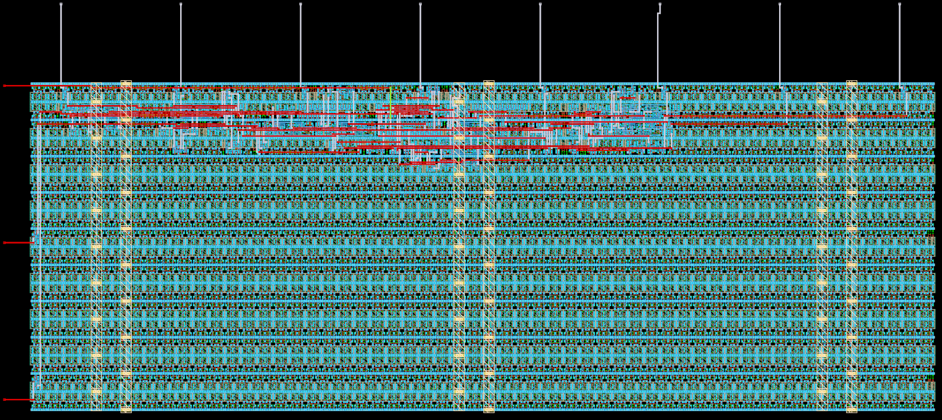
counter_top layout in KLayout (200 µm x 100 µm).
The LibreLane render is copied to render/img/counter_top_librelane.png, and the high-resolution render from lay2img.py is saved as counter_top.png in the same folder. The verification reports are written to verification/.
4.7 RTL Mixed-Signal Simulation with Xschem
For an introduction to Ngspice and Verilog RTL co-simulation with Xschem, see Stefan Schippers’ video: Ngspice + Verilog Co-Simulation in Xschem. This RTL mixed-signal simulation is currently not included in this repository, but it will be added in a future update.
4.8 Gate-Level Mixed-Signal Simulation with Xschem
A more accurate validation step is the gate-level mixed-signal simulation in Xschem with the Ngspice XSPICE event-driven engine. The gate-level Verilog netlist produced after synthesis (runs/RUN_*/*-yosys-synthesis/<TOP>.nl.v) is converted into an XSPICE model with the following command.
make generate-xspiceThe conversion pipeline is .nl.v → .vp → .spice → .xspice, followed by a pin-reorder pass to match the Xschem symbol (schematic/xschem/counter_top.sym).
.vp is the gate-level Verilog netlist with power pins. Hence, one might think that the conversion could be done directly from the .pnl.v netlist in the flow/final/ folder. However, the .nl.v file from the LibreLane yosys-synthesis step must be used. The target make generate-xspice is not executed by make all.
The Xschem testbench (counter_top_tb_tran.sch) can be opened and simulated interactively.
cd testbenches/xschem
xschem counter_top_tb_tran.sch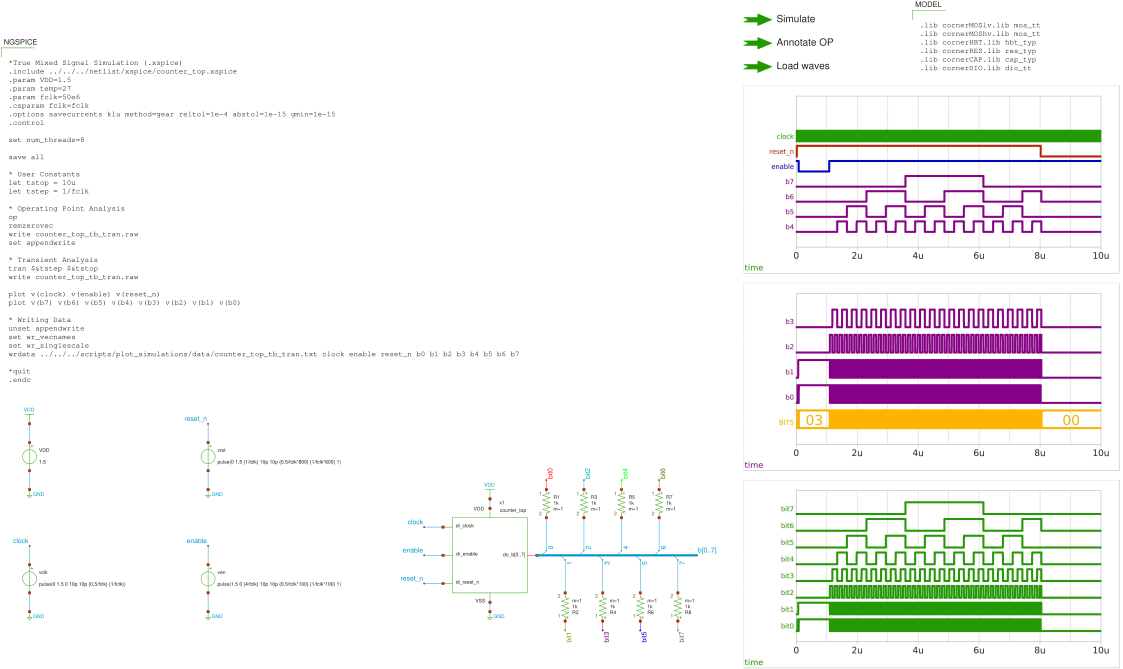
counter_top_tb_tran.
In Xschem, hold Ctrl and click the Simulate button in the schematic to launch the simulator. Once the simulation has finished, you can hold Ctrl and click the Load waves arrow to load the simulation results into the integrated waveform viewer.
This testbench also shows multiple ways to connect and display bus signals in Xschem. For more information, refer to the Xschem documentation: Use Bus/Vector notation for signal bundles / arrays of instances.
The green arrows in Xschem are called “launchers” and are essentially a series of Tcl commands. Since Xschem is fully scriptable via Tcl, repetitive tasks can be easily automated. Select a launcher and press q (Properties) to inspect or modify its underlying Tcl commands. This is also the beauty of Xschem and the reason why it is possible to also run simulations non-interactively, generate netlists, and run LVS with only Makefile targets, as you will see below.
The same simulation can also be run non-interactively from the Makefile, and the result can be plotted from Python.
make sim-gl-xschem
make sim-view-xschem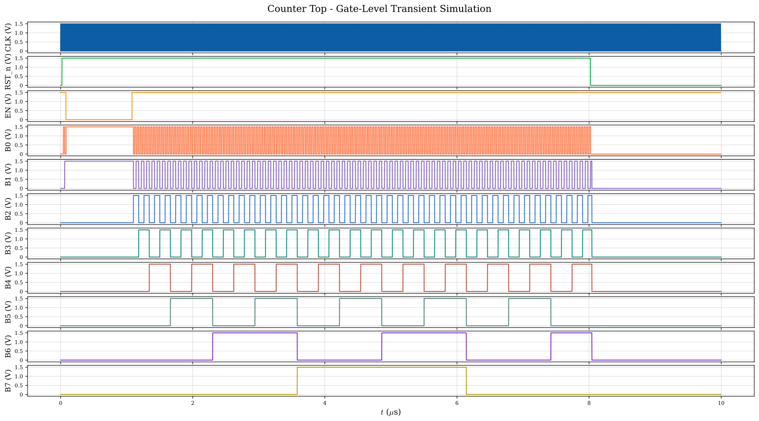
counter_top_tb_tran from scripts/plot_simulations/plot_counter_top.py.
4.9 Build and Verify Everything
The full lint, simulation, and build chain is run with the following command.
make allThis calls lint-verilog-all, sim-all, build-fpga, and build-top in sequence. LVS and DRC are already covered by the LibreLane verification steps, so no extra verification target is needed for the digital macro.
5 Analog Macro Implementation
The inverter macro is the analog reference macro of the template. It is a four-channel CMOS inverter, drawn at transistor level, and verified with a comprehensive verification chain:
- Layout vs. Schematic (LVS) with KLayout or Magic + Netgen,
- Design Rule Checking (DRC) with KLayout or Magic,
- Parasitic Extraction (PEX) with Magic + Netgen,
- Monte Carlo simulation of process and mismatch variations with CACE.
Two instances are used in the chip core. One is used as a 4-channel digital inverter (inverter1), and the other as a 2-channel analog inverter (inverter2). See the chip specifications for the full picture.
An inverter can act as a digital circuit (when the input is driven by a digital signal and the output is switching between the supply rails). Here, we characterize the inverter as an analog circuit, meaning that we are interested in its continuous voltage transfer characteristic and its small-signal voltage gain.
5.1 Directory Structure
The inverter design files are located in macros/inverter/, and the relevant folders are:
| Folder | Content |
|---|---|
schematic/xschem/ |
Xschem schematics and symbols (inverter.sch, inverter.sym, inverter_top.sch, inverter_top.sym, inverter_top_pex.sym). |
layout/ |
KLayout GDS files (*.klay.gds) and the exported inverter_top.gds. |
testbenches/xschem/ |
Transient, ac open-loop, dc input sweep, and top-level transient testbenches. |
netlist/ |
schematic/ (CDL for KLayout LVS / SPICE for Magic + Netgen LVS), layout/ (extracted for LVS), pex/ (SPICE). |
scripts/ |
Python plotters, sizing notebooks, layout rendering, PEX pin reordering. |
verification/ |
drc/, lvs/, and cace/ (process, mismatch, supply sweeps). |
final/ |
Build deliverables for the top-level integration (LEF, LIB, Verilog stub, GDS). |
render/ |
Macro renders for documentation. |
Read the inverter README first to get familiar with the folder layout and the available Makefile targets. Most of the commands below are documented there as well.
5.2 Schematic-Level Simulation
Go to the Xschem testbench folder and start Xschem.
cd macros/inverter/testbenches/xschem
xschem
xschem <testbench_name>.sch # load a testbench schematic directly at startup
Four testbenches are available in testbenches/xschem/.
inverter_tb_tran.sch, single-channel transient response (see Figure 8),inverter_tb_ac_ol.sch, open-loop ac characterisation (see Figure 9),inverter_tb_dc_vout.sch, dc input sweep (see Figure 10),inverter_top_tb_tran.sch, top-level transient oninverter_top(see Figure 11).
Load a testbench in Xschem by pressing Ctrl + o, then hold Ctrl and click the Simulate button in the schematic to launch the simulator. Once the simulation has finished, hold Ctrl and click the Load waves arrow to load the results into the integrated waveform viewer. The following figures show the testbench schematics and selected plotted results.
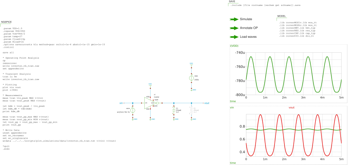
inverter_tb_tran (single-channel transient response on inverter).
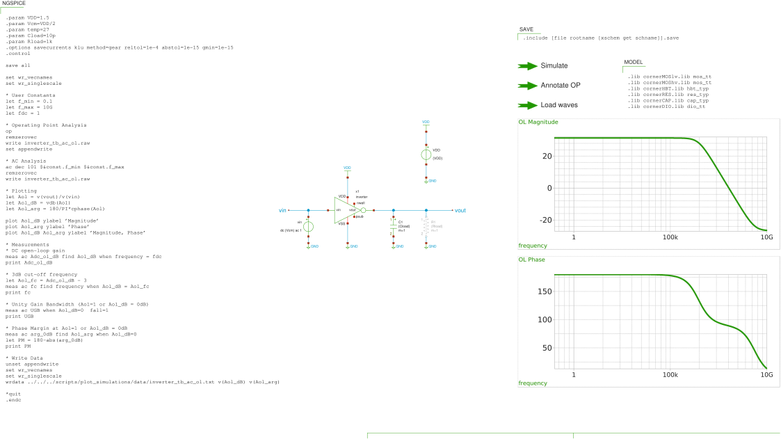
inverter_tb_ac_ol (open-loop ac characterisation on inverter).
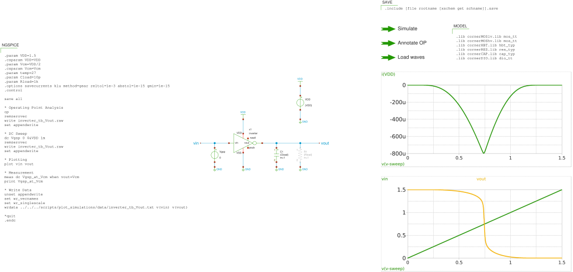
inverter_tb_dc_vout (dc input sweep on inverter).
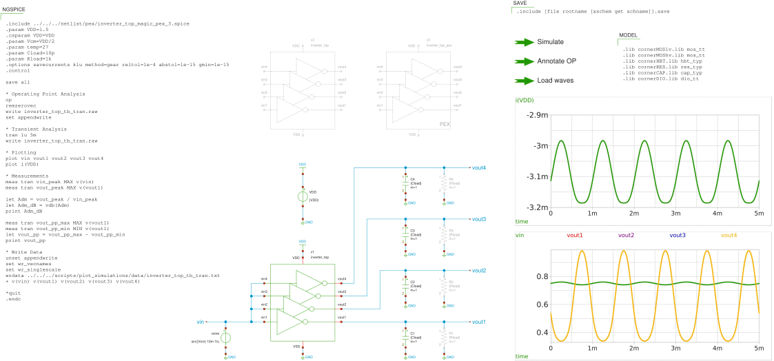
inverter_top_tb_tran (transient on inverter_top).
Non-interactive runs and post-processing are also available through the Makefile.
cd macros/inverter
make sim-xschem TB=<testbench_name>     # run a specific testbench non-interactively
make sim-view-xschem CELL=inverter      # plot results of inverter with Python
make sim-view-xschem CELL=inverter_top  # plot results of inverter_top with Python
The Makefile target sim-view-xschem calls the Python plotters in scripts/plot_simulations/ to parse the raw simulation output and plot the results with Matplotlib. The following figures show some of these plotted results.
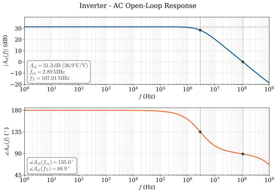
inverter_tb_ac_ol.
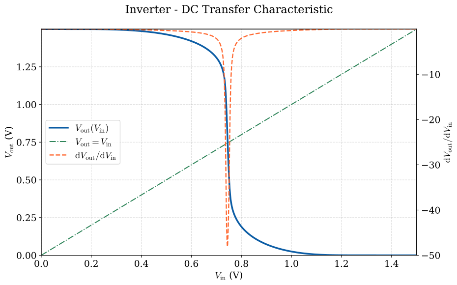
inverter_tb_dc_vout.
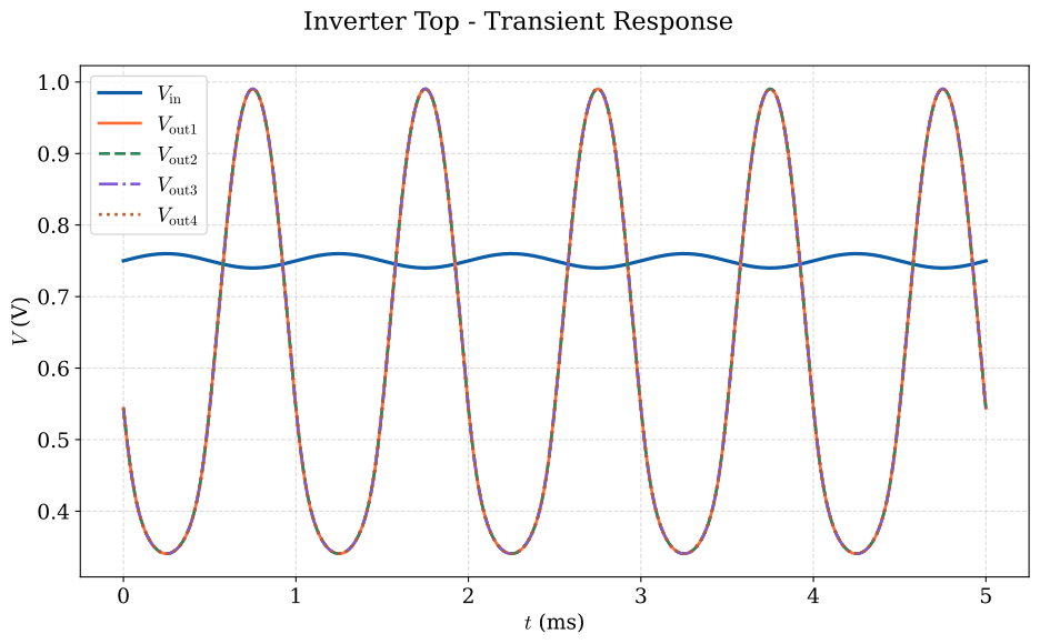
inverter_top_tb_tran.
The full simulation suite, including all four testbenches plus the CACE flow (see Section 5.4), is triggered with make sim-all.
5.3 Schematic-Level Drawing
To inspect or modify the underlying circuit of a symbol, mark the symbol and press e to descend into the underlying circuit, then Ctrl + e to go back up. To inspect or modify the graphical symbol of a device, mark the symbol and press i to descend into the symbol drawing, then Ctrl + e to go back up again.
Since Xschem is a text-based schematic editor, you can also add *.sch and .sym files in a text editor and modify them there. This is especially useful for search-and-replace operations.
Figure 15 shows the symbol of the inverter cell.
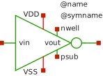
inverter symbol.
Figure 16 displays the schematic of the inverter cell with additional small-signal parameters for the NMOS and PMOS transistors at the chosen operating point. To view these small-signal parameters, hold Ctrl and click Annotate OP after the simulation has finished. Afterwards, descend into the inverter schematic.
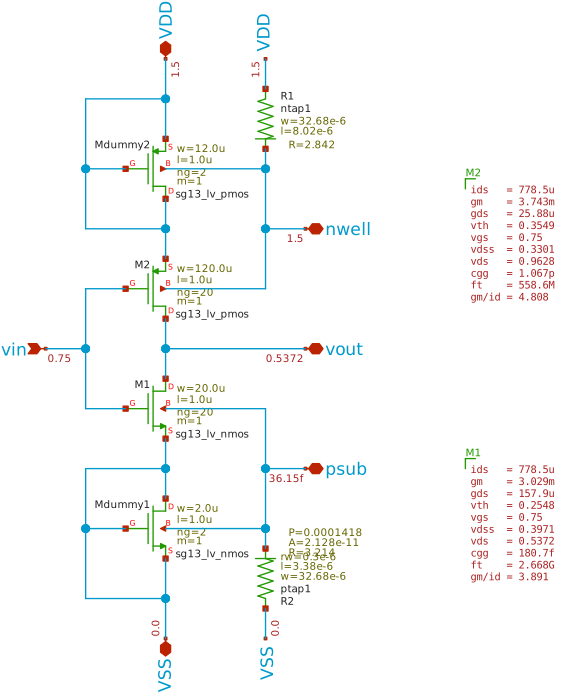
inverter schematic with dummy transistors and OP annotations.
The devices ntap and ptap are the NMOS and PMOS substrate contacts, which are required for a successful KLayout LVS and have no impact on the circuit functionality. This approach is only used by the ihp-sg13g2 PDK and is controversial since it requires additional pins nwell and psub and overloads the schematic drawings.
5.4 Process Variation and Mismatch (CACE)
CACE drives Ngspice via a characterisation YAML file (verification/cace/inverter.yaml) to run Monte-Carlo simulations and produce process and mismatch variation plots.
make sim-cacePlots are written to verification/cace/results/inverter/. This step is mainly relevant for advanced designers who want to characterise the analog macro across PVT corners. The following figures show the results of the CACE simulations for 200 iterations.
Figure 17 shows the process (left) and mismatch (right) variations of the dc open-loop gain \(A_\mathrm{ol}\), while Figure 18 plots its variation across several process corners at one fixed supply voltage.
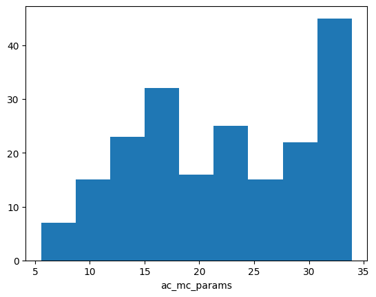
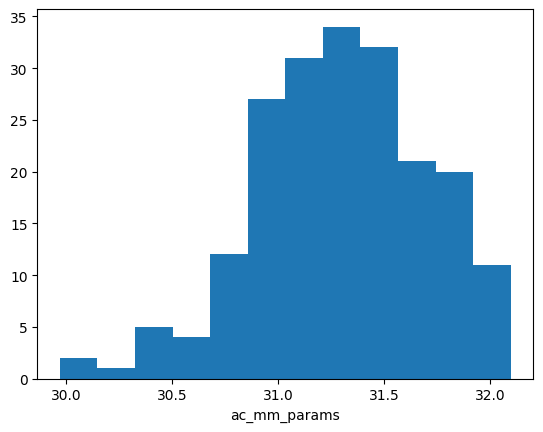
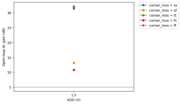
Figure 19 shows the process (left) and mismatch (right) variations of the open-loop lower cut-off frequency \(f_\mathrm{cu}\), while Figure 20 plots its variation across several process corners at one fixed supply voltage.
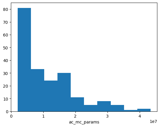
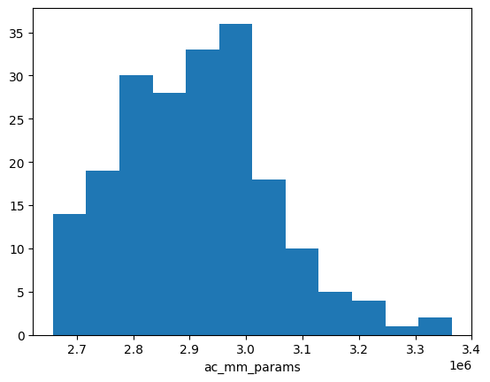
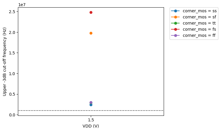
Note that the above process and mismatch variation results are poor for an analog circuit. Also, the open-loop gain varies significantly across corners. This is because the example is only a simple inverter without a compensation technique. For a practical single-ended inverter amplifier, one would at least add a feedback resistor from output to input to stabilise the operating point and therefore the gain across corners. If you want to see improved variation results, you can try adding a feedback resistor in the inverter.sch schematic and running the CACE flow again.
In the inverter.yaml characterisation file, more parameter sweeps can be added, for example, across temperature, supply voltages or load capacitance.
5.5 Transistor Sizing
During simulation, it could happen that some specifications are not fulfilled and that the inverter must be resized. In this tutorial, the inverter is sized with the \(g_\mathrm{m}/I_\mathrm{D}\) method (see Transistor Sizing Using \(g_\mathrm{m}/I_\mathrm{D}\) Methodology for theoretical background). Instead of relying on textbook square-law equations, the method looks up the actual device behaviour from pre-characterised SPICE simulations, parametrised by \(g_\mathrm{m}/I_\mathrm{D}\). An overview of these techsweeps can be found in the folder doc/sizing/. The chosen \(g_\mathrm{m}/I_\mathrm{D}\) point sets the inversion level of the transistor and therefore the trade-off between intrinsic gain (high \(g_\mathrm{m}/I_\mathrm{D}\), weak inversion) and bandwidth (low \(g_\mathrm{m}/I_\mathrm{D}\), strong inversion). An overview of the \(g_\mathrm{m}/I_\mathrm{D}\) tradeoffs can be found here. For each chosen operating point the lookup tables return all relevant figures of merit (\(I_\mathrm{D}/W\), \(g_\mathrm{m}/g_\mathrm{ds}\), \(g_\mathrm{m}/C_\mathrm{gg}\), \(S_\mathrm{TH}\), etc.) at the actual bias condition, which is then used to compute \(W\) for a given drain current.
The full sizing flow for the inverter is implemented in the Jupyter notebook scripts/sizing/sizing_inverter.ipynb. The notebook uses pygmid to query the pre-characterised ihp-sg13g2 NMOS/PMOS lookup tables (sg13g2_lv_nmos.mat and sg13g2_lv_pmos.mat). An overview of the \(g_\mathrm{m}/I_\mathrm{D}\) MOSFET characterization procedure can be found here.
The Jupyter notebook sizing_inverter.ipynb runs through the following steps:
- Define the design targets: \(V_\mathrm{DD} = 1.5\,\mathrm{V}\), \(V_\mathrm{cm,in} = V_\mathrm{cm,out} = V_\mathrm{DD}/2 = 0.75\,\mathrm{V}\), \(I_\mathrm{out} = 0.75\,\mathrm{mA}\), \(C_\mathrm{load} = 10\,\mathrm{pF}\) and \(L = 1\,\mathrm{\upmu m}\). \(L\) is chosen longer than the minimum to increase intrinsic gain and reduce mismatch, but at the cost of increased area and reduced bandwidth.
- Look up \(g_\mathrm{m}/I_\mathrm{D}\), \(g_\mathrm{m}/g_\mathrm{ds}\), \(g_\mathrm{m}/C_\mathrm{gg}\) and \(I_\mathrm{D}/W\) based on \(L\) and the operating-point voltages.
- Compute the required widths \(W = I_\mathrm{D} / (I_\mathrm{D}/W)\) for NMOS and PMOS, and derive the resulting \(W_\mathrm{PMOS}/W_\mathrm{NMOS}\) ratio.
- Round the continuous widths to a practical finger configuration with equal finger counts for NMOS and PMOS (for better layout matching) and recompute the small-signal parameters with the final widths.
- Estimate the open-loop gain \(A_\mathrm{ol} = -g_\mathrm{m,tot} / g_\mathrm{ds,tot}\) and the output resistance \(R_\mathrm{out} = 1/g_\mathrm{ds,tot}\) of the complementary inverter stage.
The resulting device geometry is summarised in Table 1.
| Device | \(L\) (\(\mathrm{\upmu m}\)) | Fingers (\(\mathrm{NF}\)) | \(W\) / Finger (\(\mathrm{\upmu m}\)) | Total \(W\) (\(\mathrm{\upmu m}\)) |
|---|---|---|---|---|
| NMOS \(M_1\) | 1.0 | 20 | 1.0 | 20.0 |
| PMOS \(M_2\) | 1.0 | 20 | 6.0 | 120.0 |
With these final widths the notebook computes the small-signal parameters listed in Table 2. As a reference, compare these values with the OP annotations in Figure 16.
| Parameter | NMOS \(M_1\) | PMOS \(M_2\) | Inverter (NMOS \(\parallel\) PMOS) |
|---|---|---|---|
| Drain current \(I_\mathrm{D}\) (\(\mathrm{mA}\)) | 0.89 | 0.78 | – |
| Transconductance efficiency \(g_\mathrm{m}/I_\mathrm{D}\) (\(\mathrm{V^{-1}}\)) | 3.76 | 3.76 | – |
| Inversion level | strong | strong | – |
| Transconductance \(g_\mathrm{m}\) (\(\mathrm{mS}\)) | 3.35 | 2.92 | – |
| Output conductance \(g_\mathrm{ds}\) (\(\mathrm{\upmu S}\)) | 116 | 29 | – |
| Gate capacitance \(C_\mathrm{gg}\) (\(\mathrm{fF}\)) | 154.32 | 824.86 | – |
| Transit frequency \(f_\mathrm{T} = g_\mathrm{m}/(2\pi\,C_\mathrm{gg})\) (\(\mathrm{GHz}\)) | 2.91 | 0.54 | – |
| Thermal noise PSD \(S_\mathrm{TH}\) at \(1\,\mathrm{Hz}\) (\(\mathrm{pV^2/Hz}\)) | 38.95 | 73.98 | – |
| Flicker corner frequency \(f_\mathrm{co}\) (\(\mathrm{MHz}\)) | 3.87 | 2.28 | – |
| \(g_\mathrm{m,tot} = g_\mathrm{m,NMOS} + g_\mathrm{m,PMOS}\) (\(\mathrm{mS}\)) | – | – | 6.28 |
| \(g_\mathrm{ds,tot} = g_\mathrm{ds,NMOS} + g_\mathrm{ds,PMOS}\) (\(\mathrm{\upmu S}\)) | – | – | 145 |
From these values, the open-loop dc gain \(A_\mathrm{ol}\), the output resistance \(R_\mathrm{out}\), the open-loop cut-off frequency \(f_\mathrm{cu}\), and the unity-gain frequency \(f_\mathrm{T}\) with a dominant capacitive load \(C_\mathrm{load} = 10\,\mathrm{pF}\) can be estimated as
\[ |A_\mathrm{ol}| = \frac{g_\mathrm{m,tot}}{g_\mathrm{ds,tot}} = \frac{6.28\,\mathrm{mS}}{145\,\mathrm{\upmu S}} = 43.2 = 32.72\,\mathrm{dB}, \]
\[ R_\mathrm{out} = \frac{1}{g_\mathrm{ds,tot}} = \frac{1}{145\,\mathrm{\upmu S}} = 6.89\,\mathrm{k\Omega}, \]
\[ f_\mathrm{cu} = \frac{1}{2\pi\,R_\mathrm{out}\,C_\mathrm{load}} = \frac{1}{2\pi \cdot 6.89\,\mathrm{k\Omega} \cdot 10\,\mathrm{pF}} = 2.31\,\mathrm{MHz}, \]
\[ f_\mathrm{T} = \frac{g_\mathrm{m,tot}}{2\pi\,C_\mathrm{load}} = \frac{6.28\,\mathrm{mS}}{2\pi \cdot 10\,\mathrm{pF}} = 100\,\mathrm{MHz}. \]
Table 3 compares these hand-calculated values against the open-loop ac simulation result from inverter_tb_ac_ol (see Figure 12).
| Quantity | \(g_\mathrm{m}/I_\mathrm{D}\) calculation | ac open-loop simulation |
|---|---|---|
| Open-loop dc gain \(A_\mathrm{ol}\) | \(32.72\,\mathrm{dB}\) | \(31.33\,\mathrm{dB}\) |
| Open-loop cut-off frequency \(f_\mathrm{cu}\) | \(2.31\,\mathrm{MHz}\) | \(2.89\,\mathrm{MHz}\) |
| Unity-gain frequency \(f_\mathrm{T}\) | \(100\,\mathrm{MHz}\) | \(107\,\mathrm{MHz}\) |
The notebook is fully parametric. Changing \(L\), the target \(g_\mathrm{m}/I_\mathrm{D}\) or \(I_\mathrm{out}\) and re-running the cells immediately produces a new sizing point, so it can be used as a starting template for sizing other simple analog blocks with the ihp-sg13g2 lookup tables. Try it out yourself by decreasing the transistor length to \(L = 0.5\,\mathrm{\upmu m}\) and see how the small-signal parameters and the resulting open-loop gain and cut-off frequency change. What would you expect based on the tradeoffs above?
5.6 Inspect / Edit the Layout
After the schematic is finalised and the design targets are met, the layout can be created. The layout of the inverter cell is hierarchical, and the top-level cell inverter_top contains four instances of the inverter cell. Around the four-channel inverter layout, a power ring is drawn on Metal5 and TopMetal1 layers, which is connected to the VDD and VSS pins of the four inverters. This power ring is required for top-level integration, connecting the macro power to the chip’s PDN.
The layout is created and edited in KLayout. The container provides the ke alias for klayout -e (edit mode). With the following command, the GDS of the four-channel inverter is opened in KLayout as shown Figure 21. With the keys 0, 1, 2, …, 9 you can view different layers as explained in the KLayout cheatsheet or in the klayout-layer-shortcuts plugin.
ke layout/inverter_top.klay.gdsAfter modifying the layout, export a clean .gds file (for example inverter_top.gds) by pressing File > Export Layout For Tapeout. The Magic-based verification flows only work on .gds files, while the KLayout-based verification flows accept either .gds or .klay.gds.
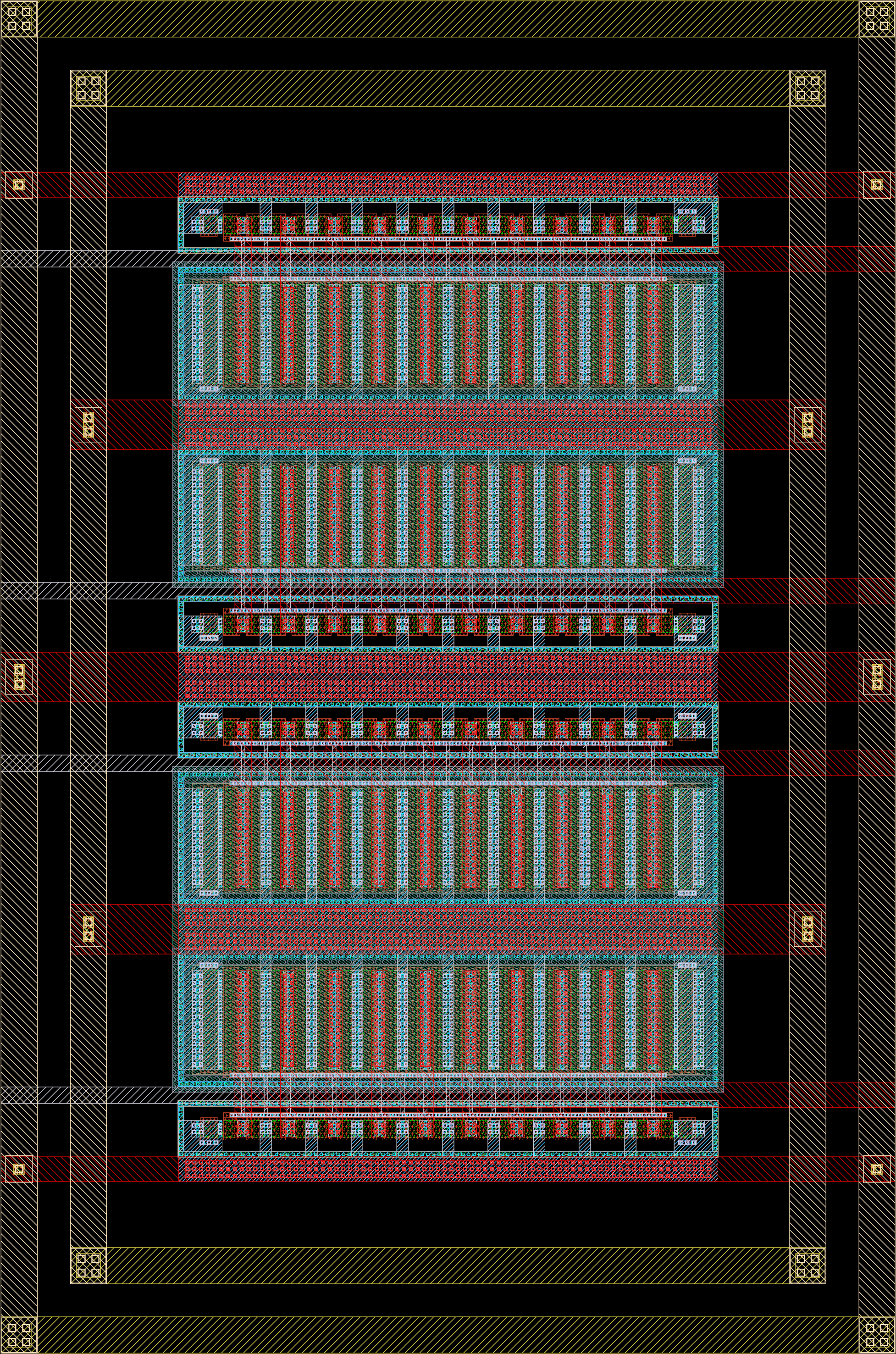
inverter_top layout in KLayout.
KLayout also supports a 2.5D viewer, which can be used to inspect the layout. To open the 2.5D viewer, press SG13G2 PDK > BEOL 2.5D Viewer. Figure 22 shows the inverter_top layout in the 2.5D viewer.
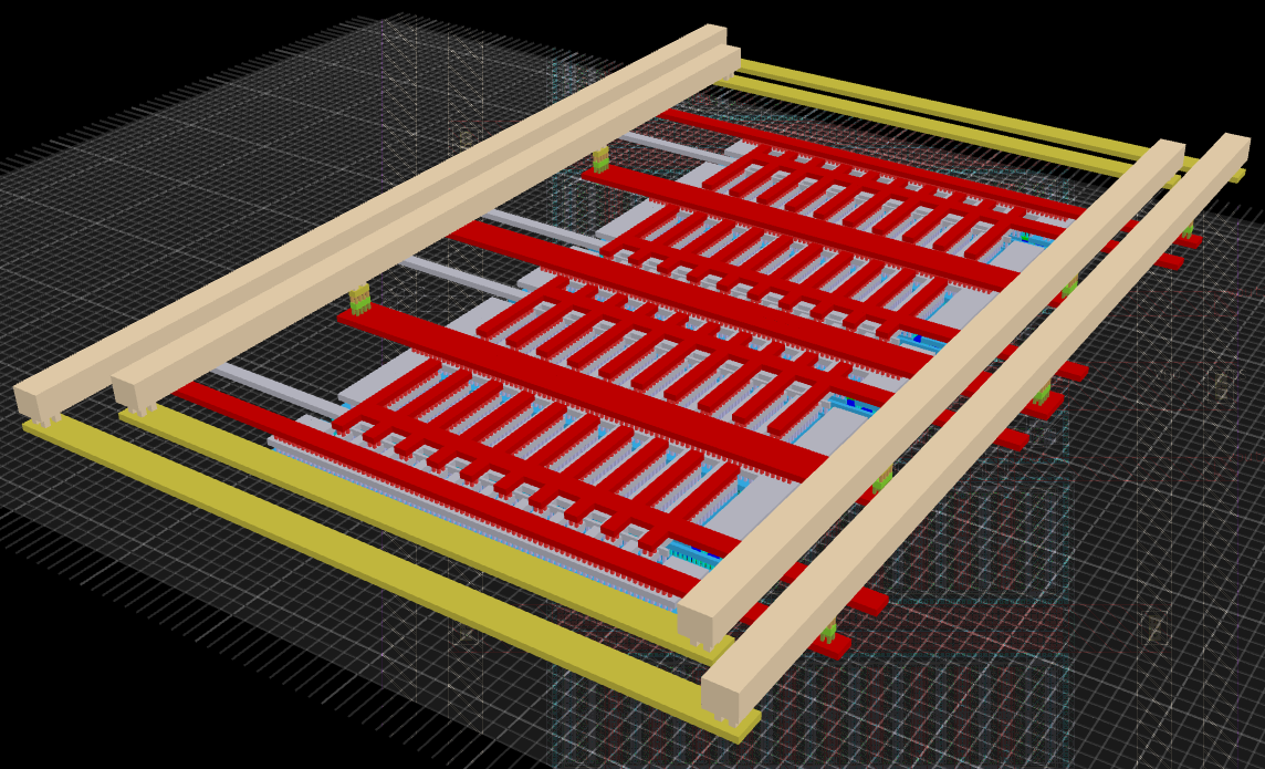
inverter_top layout in KLayout 2.5D viewer.
5.7 DRC, LVS, and PEX
The inverter macro can be verified with two verification flows, either with KLayout or with Magic + Netgen. Each flow covers DRC, LVS, and PEX. Magic + Netgen provides only non-interactive command-line flows, while KLayout also has interactive GUI-based DRC and LVS.
5.7.1 Design Rule Check
The non-interactive DRC can be run with the following Makefile targets. The CELL variable can be set to run DRC on a specific cell, or it defaults to inverter_top if not set.
make klayout-drc [CELL=<cellname>]  # default CELL=inverter_top
make magic-drc [CELL=<cellname>]    # default CELL=inverter_top
Reports are saved to verification/drc/.
In KLayout, a non-interactive DRC run can be launched from the GUI by pressing F9. The DRC options can be modified by pressing F10.
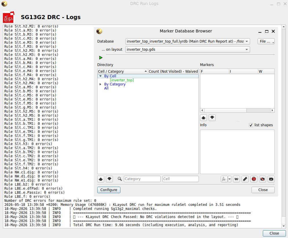
5.7.2 Layout-Versus-Schematic
The non-interactive LVS can be run with the following Makefile targets. The CELL variable can be set to run LVS on a specific cell, or it defaults to inverter_top if not set.
make klayout-lvs [CELL=<cellname>]  # default CELL=inverter_top, uses CDL netlist exported from Xschem
make magic-lvs [CELL=<cellname>]    # default CELL=inverter_top, uses SPICE netlist exported from Xschem
The schematic netlist is exported automatically by the matching *-lvs-netlist sub-target and moved to netlist/schematic/. The extracted layout netlist is moved to netlist/layout/ and the reports are saved to verification/lvs/.
In KLayout, a non-interactive LVS run can be launched from the GUI by pressing F11. The LVS options can be modified by pressing F12, where the schematic netlist inverter_top_klayout.cdl has to be selected manually. Set deep as the run mode.
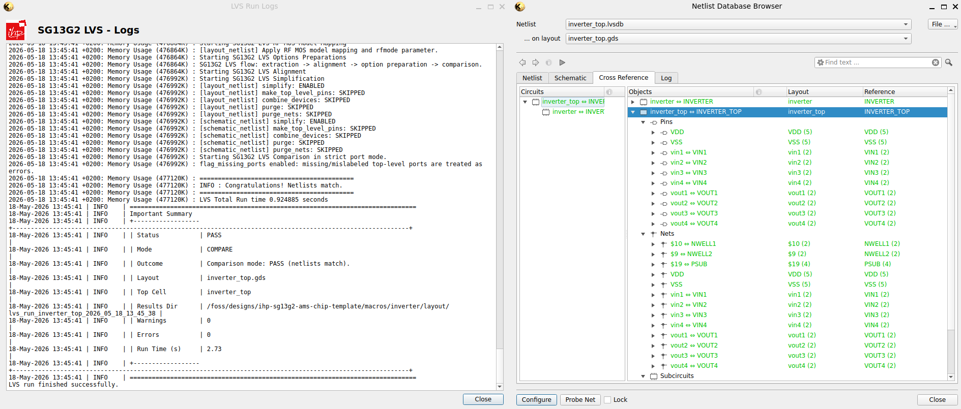
5.7.3 Parasitic Extraction
The non-interactive PEX can be run with the following Makefile targets. The CELL variable can be set to run PEX on a specific cell, or it defaults to inverter_top if not set. The EXT_MODE variable can be set to choose between different extraction modes,
EXT_MODE=1for C-decoupled mode,EXT_MODE=2for C-coupled mode,EXT_MODE=3for full-RC extraction.
If not set, it defaults to EXT_MODE=3.
make klayout-pex [CELL=<cellname>] [EXT_MODE=<1|2|3>]   # default CELL=inverter_top, default EXT_MODE=3 (full-RC)
make magic-pex [CELL=<cellname>] [EXT_MODE=<1|2|3>]     # default CELL=inverter_top, default EXT_MODE=2 (CC mode)
PEX writes a SPICE netlist into netlist/pex/. The subcircuit name is renamed to <CELL>_pex, and the pin order is rearranged to match the Xschem PEX symbol (inverter_top_pex.sym).
To run a post-layout simulation, open one of the Xschem testbenches, swap the original symbol with the PEX symbol, and include the path to the SPICE netlist so the extracted netlist is used in the same testbench. This is the recommended way to compare schematic-only and post-layout simulation results.
Note that KLayout-PEX (KPEX) is currently under development and therefore the Magic engine is used internally for the actual extraction.
5.7.4 Run Full Verification Flow at Once
If you want to run the full verification flow at once, the verify targets bundle LVS, DRC, and PEX in one command.
make klayout-verify [CELL=<cellname>]   # default CELL=inverter_top
make magic-verify [CELL=<cellname>]     # default CELL=inverter_top
5.8 Build Deliverables for Top-Level Integration
For the inverter to be picked up by the top-level LibreLane flow, it must expose a LEF (abstract pin / blockage view), a Liberty timing library stub, and a Verilog stub. The Verilog stub is referenced by rtl/chip_top.sv for top-level integration. These files can be built with individual Makefile targets or via build-top.
make lef          # final/lef/inverter_top.lef
make lib          # final/lib/inverter_top.lib
make verilog      # final/vh/inverter_top.v
make build-top    # the three steps above plus copy-gds and render-gds
make build-top also copies the GDS to final/gds/ and renders the macro to render/img/inverter_top.png, as displayed in Figure 21.
5.9 Full Analog Macro Flow
The full simulation, build, and verification chain is run with the following command.
make allThis calls sim-all (Xschem + CACE), klayout-verify-all, magic-verify-all, and build-top in sequence. Depending on the hardware used, a full pass can take a few minutes, especially the CACE simulation step.
6 Bondpad and Logo Implementation
The ip/ folder holds the three custom IP cells that the top-level chip relies on: a bondpad and two logos. These IPs are generated and require zero hand drawing. Each IP ships with a Python script and Makefile targets that produce the final GDS and LEF, and run KLayout and Magic DRC. This makes it easy to re-spin a different bondpad size or shape, swap the logo image, or move the artwork to another metal layer without touching layout tools.
The three IP cells covered in this section are:
sg13g2_ip__bondpad_70x70, a 70 µm × 70 µm square bondpad built from IHP’sSG13_devKLayout PCell library,sg13g2_ip__jku, the Johannes Kepler University Linz logo, generated from a PNG image,sg13g2_ip__jku_names, a companion text block with the names of the institute, generated the same way as the JKU logo.
All three IPs follow the same folder structure (script/, final/, verification/) and the same Makefile conventions as the digital and analog macros (make help, make all, make clean, make klayout-drc, make magic-drc). The logo folders sg13g2_ip__jku and sg13g2_ip__jku_names have an additional logo/ folder that contains the source PNG image.
6.1 Directory Structure
The IP design files are located in ip/, and the relevant folders are:
| Folder | Content |
|---|---|
sg13g2_ip__bondpad_70x70/script/ |
KLayout Python script (bondpad.py) that instantiates the SG13_dev::bondpad PCell and writes the GDS and LEF. |
sg13g2_ip__jku/logo/ and sg13g2_ip__jku_names/logo/ |
Source PNG images (jku_logo.png, jku_names.png) for the two logos. |
sg13g2_ip__jku/script/ and sg13g2_ip__jku_names/script/ |
PNG-to-GDS converter (make_gds.py) shared by both logos. |
final/gds/, final/lef/, final/lib/, final/vh/ |
Build deliverables for top-level integration: GDS, LEF, Liberty, and Verilog blackbox stubs. |
verification/drc/ |
DRC reports produced by make klayout-drc and make magic-drc. |
Read the bondpad README, the JKU logo README, and the JKU names README first to get familiar with the Makefile targets and parameters. Most of the commands below are also documented there.
6.2 Bondpad Generation
The bondpad is generated by the Python script script/bondpad.py, which runs in KLayout batch mode (klayout -zz). It
- instantiates the
bondpadPCell from IHP’sSG13_devlibrary, - flattens the PCell into a static top cell,
- writes the layout as a GDSII file, and
- generates a matching LEF macro description for OpenROAD / LibreLane.
Geometry and metal stack are parametrised through three Makefile variables. The defaults match the chip’s padframe and the SG13G2 PDK defaults.
| Variable | Default | Description |
|---|---|---|
DIAMETER |
70.0 |
Bondpad diameter / side length in µm. |
SHAPE |
square |
Pad geometry. Allowed: square, octagon, circle. |
BOTTOM_METAL |
3 |
Lowest metal in the pad stack: 1=Metal1 .. 5=Metal5, 6=TopMetal1. Top is fixed to TopMetal2. Default 3 matches bondpad_bottomMetal in sg13g2_tech.json. |
The available Makefile targets for the bondpad are summarised below.
| Target | What it does |
|---|---|
bondpad |
Generate GDS and LEF via bondpad.py (make bondpad [DIAMETER=<um>] [SHAPE=<square\|octagon\|circle>] [BOTTOM_METAL=<1-6>]). |
verilog |
Generate a Verilog blackbox stub. |
klayout-drc |
Run KLayout DRC (make klayout-drc [CELL=<cellname>]). |
magic-drc |
Run Magic DRC (make magic-drc [CELL=<cellname>]). |
clean |
Remove the final/ and verification/drc/ output directories. |
To execute the clean, bondpad, verilog, klayout-drc, and magic-drc targets in sequence, run:
cd ip/sg13g2_ip__bondpad_70x70
make all
View the bondpad layout in KLayout with:
ke final/gds/sg13g2_ip__bondpad_70x70.gds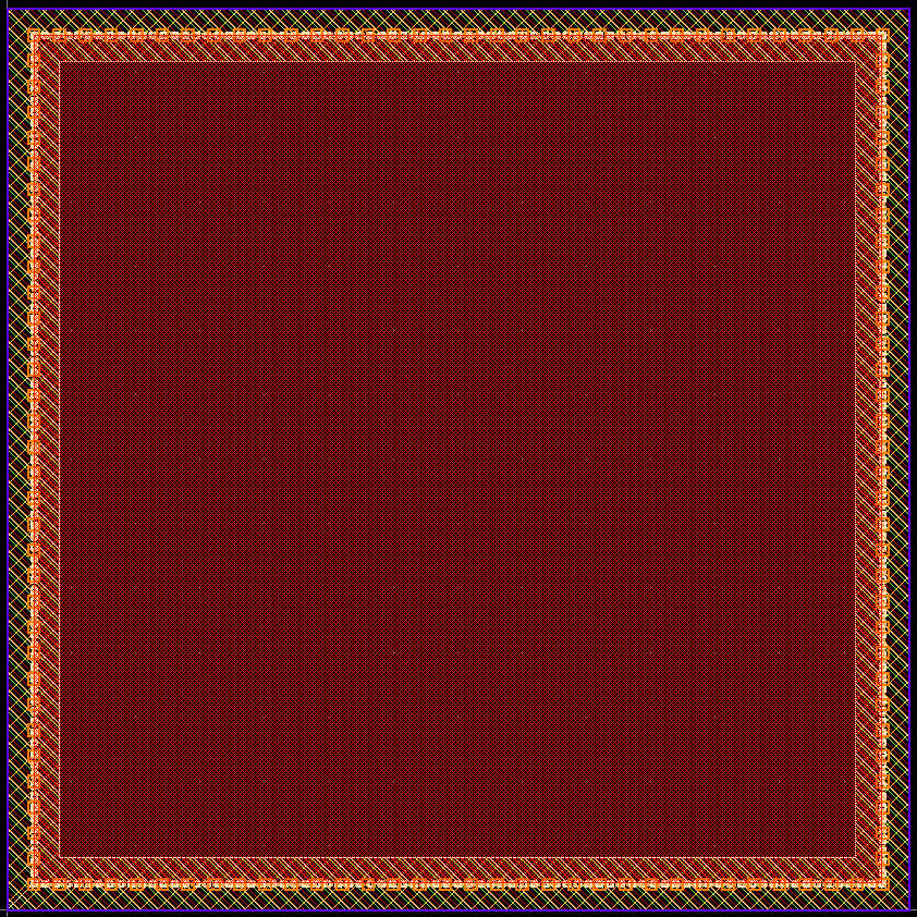
sg13g2_ip__bondpad_70x70 layout in KLayout.
The bondpad goes from Metal3 up to TopMetal2 by default, but the BOTTOM_METAL Makefile variable can be set to change the lowest metal in the stack. The pad is surrounded by the pad recognition layer dfpad (41, 0).
The bondpad target accepts the geometry and metal-stack variables as command-line overrides. For example, to build an octagonal 80 µm bondpad from Metal2 up to TopMetal2, run:
make bondpad DIAMETER=80 SHAPE=octagon BOTTOM_METAL=26.3 Logo Generation
Both logo IPs share the same Makefile targets and PNG-to-GDS converter script/make_gds.py, built on the klayout.db Python module. The conversion proceeds in five steps:
- Open the source PNG (
logo/jku_logo.pngorlogo/jku_names.png) and convert it to a binary mask using a brightness threshold (default128). - Optionally invert the mask (
--invert) so that the dark logo regions become the foreground. - For each foreground pixel, draw a square of side
--pixel-sizeµm on the selected metal layer. - Merge adjacent rectangles into larger polygons (
--merge) to keep the GDS small and DRC-friendly. - Add the block-bounding rectangle on the boundary layers
prBoundary(189/0) andNoMetFiller(160/0).
The Makefile derives the foreground GDS layer number (e.g. 67/0 for Metal5) and the LEF obstruction layer name from the same LAYER variable, so the artwork in the GDS and the blockage exposed to the router always stay consistent.
Both logos share the same set of Makefile variables as shown below. The jku_names logo uses a finer standard pixel size to ensure the readability of the smaller text elements.
| Variable | Default (jku / jku_names) |
Description |
|---|---|---|
IMG_SIZE_PX |
750 / 750 |
Source image side length in pixels. Used to compute the scale factor automatically. |
BLOCK_SIZE |
100 / 100 |
Physical side length of the rendered logo in µm. |
PIXEL_SIZE |
0.50 / 0.25 |
Edge of one rendered pixel in µm. Must stay ≥ the layer’s minimum width (0.21 µm on Metal5). |
LAYER |
Metal5 / Metal5 |
Foreground metal layer. One of Metal1..Metal5, TopMetal1, TopMetal2. |
The image scale factor is computed automatically as BLOCK_SIZE / (IMG_SIZE_PX * PIXEL_SIZE), so changing any of the three keeps the rendered block at the target physical size.
The available Makefile targets for the logos are summarised below.
| Target | What it does |
|---|---|
logo |
Convert the PNG into a GDSII layout using make_gds.py. |
lef |
Emit a minimal LEF macro (CLASS BLOCK, full-area OBS on LAYER_NAME). |
lib |
Emit a Liberty timing stub (empty cell) so the LibreLane flow can pick the cell up. |
verilog |
Emit a Verilog blackbox stub (module sg13g2_ip__jku;) with no ports. |
klayout-drc |
Run KLayout DRC (same relaxed rule-set as the bondpad). |
magic-drc |
Run Magic DRC. |
clean |
Remove final/ and verification/drc/. |
To execute the clean, logo, lef, lib, verilog, klayout-drc, and magic-drc targets in sequence, run:
cd ip/sg13g2_ip__jku                # or ip/sg13g2_ip__jku_names
make all
View the JKU logo or JKU names layout in KLayout with:
ke final/gds/sg13g2_ip__jku.gds # or sg13g2_ip__jku_names.gds
sg13g2_ip__jku logo.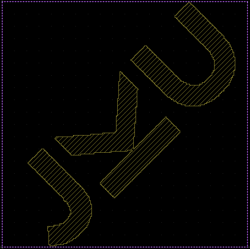
sg13g2_ip__jku layout in KLayout.sg13g2_ip__jku logo (left) and sg13g2_ip__jku layout in KLayout (right).
To replace the logo with your own artwork, drop a square PNG image into logo/ and either rename it to jku_logo.png / jku_names.png, or override IMG_FILE in the Makefile. A clean black-on-white image with a few hundred pixels per side and high contrast works best.
6.4 Top-Level Assembly
For top-level assembly, the top-level Makefile exposes two wrapper targets that descend into the IP folders and call make all:
make build-bondpad      # build ip/sg13g2_ip__bondpad_70x70
make build-logos        # build ip/sg13g2_ip__jku and ip/sg13g2_ip__jku_names
Both targets are part of make build-all (see Section 7), so the IP cells are refreshed automatically before the chip is hardened with LibreLane. The generated GDS, LEF, Verilog stub and Liberty files are referenced by flow/librelane/config.yaml when assembling the chip top-level. Furthermore, the Verilog stubs are instantiated in rtl/chip_top.sv.
7 Top-Level Implementation
This section covers the top-level assembly and padframe generation. The top-level files that need to be understood and modified for a new chip are:
rtl/chip_top.sv, the padframe wrapper. It instantiates one I/O cell per pad and exposes the globalclk_PAD,rst_n_PAD,input_PAD,output_PAD,bidir_PAD, andanalog_PADsignals.rtl/chip_core.sv, the core logic. It instantiates the digital and analog macros (counter1,counter2,inverter1,inverter2,sram_0) and wires them together and to the I/O pads.flow/librelane/config.yaml, the top-level LibreLane configuration. It defines the padframe order (PAD_WEST,PAD_NORTH,PAD_SOUTH,PAD_EAST), the chip area (DIE_AREA,CORE_AREA), the PDN core ring (PDN_CORE_RING_VWIDTH,PDN_CORE_RING_HWIDTH,PDN_CORE_RING_VSPACINGandPDN_CORE_RING_HSPACING), the clock settings (CLOCK_PORT,CLOCK_NETandCLOCK_PERIOD), the macro list (MACROS), the bondpads, the logos, non-default routing rules (NON_DEFAULT_RULES,DRT_ASSIGN_NDR, andRSZ_DONT_TOUCH_LIST), STA corners, and references topdn_cfg.tclandchip_top.sdc.flow/librelane/pdn_cfg.tcl, the Tcl script that builds the OpenROAD PDN. The bottom of the file contains the custom PDN connects forinverter1,inverter2, andsram_0. This is the part that has to be touched when adding new macros.flow/librelane/chip_top.sdc, timing constraints (clock period, input/output delays).- Reference documentation for the chip, specifications.md, pinout.md, and floorplan.md.
7.1 Understanding chip_top.sv
The padframe wrapper chip_top.sv declares the chip’s parameters and ports. The parameter block at the top of the module controls the number of pads of each type and is the place to update when the pinout changes.
rtl/chip_top.sv (code snippet)
module chip_top #(
    // Power / ground pads for digital core / analog front-end
    parameter int unsigned NUM_VDD_PADS    = 1,
    parameter int unsigned NUM_VSS_PADS    = 1,

    // Power / ground pads for I/O
    parameter int unsigned NUM_IOVDD_PADS  = 1,
    parameter int unsigned NUM_IOVSS_PADS  = 1,

    // Signal pads
    parameter int unsigned NUM_INPUT_PADS  = 1,  // excluding clock and reset pads
    parameter int unsigned NUM_OUTPUT_PADS = 17,
    parameter int unsigned NUM_BIDIR_PADS  = 4,
    parameter int unsigned NUM_ANALOG_PADS = 4
) ( ... );
The remaining code does not need to be modified for a pinout change, since the generate blocks automatically instantiate the correct number of I/O cells based on the parameter values. One generate block per pad type (vdd_pads, vss_pads, iovdd_pads, iovss_pads, inputs, outputs, bidirs, analogs) instantiates the matching IHP I/O cell, plus single instances for the clock and reset pads. An example code snippet of the input pad generation with a generate block is shown below. The input_PAD signals are exposed as ports of the chip_top module and are connected to the pads of the I/O cell, while the input_PAD2CORE signals are connected to the internal core logic in chip_core.sv. The same structure, or a very similar one, applies to the other pad types.
Normally, only the parameter counts need to be edited in chip_top.sv. Only multi-clock and multi-reset chips would require modifications to the clock and reset pad generation, since the current template supports only one clock and one reset pad.
rtl/chip_top.sv (code snippet)
generate
    for (genvar i = 0; i < NUM_INPUT_PADS; i++) begin : g_inputs
        sg13g2_IOPadIn input_pad (
            `ifdef USE_POWER_PINS
            .iovdd (IOVDD),
            .iovss (IOVSS),
            .vdd   (VDD),
            .vss   (VSS),
            `endif
            .p2c   (input_PAD2CORE[i]),
            .pad   (input_PAD[i])
        );
    end
endgenerateThe sg13g2_IOPadAnalog cell exposes two internal core-side nodes per analog pad:
padres: path through the pad’s secondary ESD resistorpadbare: direct path to the pad metal (only primary ESD diodes)
In this template, inverter2 uses both paths:
vin1/vin2are connected toanalog_PADRES[0:1](resistor-protected input path)vout1/vout2are driven ontoanalog_PADBARE[2:3](direct output path to avoid extra RC)
Inside chip_core.sv, these nets appear as the corresponding lowercase core signals analog_padres[*] and analog_padbare[*].
rtl/chip_top.sv (code snippet)
generate
    for (genvar i = 0; i < NUM_ANALOG_PADS; i++) begin : g_analogs
        (* keep *)
        sg13g2_IOPadAnalog analog_pad (
            `ifdef USE_POWER_PINS
            .iovdd   (IOVDD),
            .iovss   (IOVSS),
            .vdd     (VDD),
            .vss     (VSS),
            `endif
            .pad     (analog_PAD[i]),
            .padres  (analog_PADRES[i]),
            .padbare (analog_PADBARE[i])
        );
    end
endgenerate
7.2 Understanding chip_core.sv
The core chip_core.sv is where the macros are instantiated and wired to the chip’s I/O pads. The enable signal is mapped to input_PAD[0], the two counter_top instances share the clock and reset, the two inverter_top instances are wired up (one digital, one analog), and the SRAM output is XOR-reduced to a single bit on output_PAD[16]. The input and output assignments at the top and bottom of the file correspond to the bit-to-role mapping documented in pinout.md. For improved clarity, every assignment is written on a separate line. Advanced designers can also use bus notation for more compact code.
rtl/chip_core.sv (code snippet)
// ======================================================
// Input Assignments
// ======================================================
logic enable;
assign enable = input_in[0];

// Inverter 1
wire inv1_din1 = bidir_in[0];
wire inv1_din2 = bidir_in[1];
wire inv1_din3 = bidir_in[2];
wire inv1_din4 = bidir_in[3];

// Inverter 2
wire inv2_vin1 = analog_padres[0];
wire inv2_vin2 = analog_padres[1];
// ======================================================
rtl/chip_core.sv (code snippet)
// ======================================================
// Output Assignments
// ======================================================
// Digital outputs
// Counter 1
assign output_out[0]  = counter1_value[0];
assign output_out[1]  = counter1_value[1];
assign output_out[2]  = counter1_value[2];
assign output_out[3]  = counter1_value[3];

// Counter 2
assign output_out[4]  = counter2_value[0];
assign output_out[5]  = counter2_value[1];
assign output_out[6]  = counter2_value[2];
assign output_out[7]  = counter2_value[3];
assign output_out[8]  = counter2_value[4];
assign output_out[9]  = counter2_value[5];
assign output_out[10] = counter2_value[6];
assign output_out[11] = counter2_value[7];

// Inverter 1
assign output_out[12] = inv1_dout1;
assign output_out[13] = inv1_dout2;
assign output_out[14] = inv1_dout3;
assign output_out[15] = inv1_dout4;

// SRAM
// Reduce the 32-bit SRAM output to a single bit by computing the parity.
// output_out[16] = 1 when an odd number of bits in sram_0_out are 1.
// output_out[16] = 0 when an even number of bits in sram_0_out are 1.
assign output_out[16] = ^sram_0_out;

// Digital bidirectionals (output side)
// Bidir output enable: drive when `enable` is high (counter visible),
// float as input when low (so external stimuli can drive inverter1).
assign bidir_out[0] = counter1_value[4];
assign bidir_oe[0]  = enable;

assign bidir_out[1] = counter1_value[5];
assign bidir_oe[1]  = enable;

assign bidir_out[2] = counter1_value[6];
assign bidir_oe[2]  = enable;

assign bidir_out[3] = counter1_value[7];
assign bidir_oe[3]  = enable;

// Analog outputs
assign analog_padbare[2] = inv2_vout1;
assign analog_padbare[3] = inv2_vout2;
// ======================================================
7.3 Understanding config.yaml
The top-level LibreLane configuration config.yaml covers the following sections and references pdn_cfg.tcl and chip_top.sdc.
- Padframe generation.
PAD_WEST,PAD_NORTH,PAD_SOUTH, andPAD_EAST, in the order documented indoc/pinout.md. - PDN core ring.
PDN_CORE_RING,PDN_CORE_RING_VWIDTH,PDN_CORE_RING_HWIDTH,PDN_CORE_RING_VSPACING, andPDN_CORE_RING_HSPACING. - Clock settings.
CLOCK_PORT,CLOCK_NET, andCLOCK_PERIOD. - STA corners.
nom_fast_1p32V_m40Cnom_fast_1p65V_m40Cnom_slow_1p08V_125Cnom_slow_1p35V_125Cnom_typ_1p20V_25Cnom_typ_1p50V_25C
- Non-default routing rules.
NON_DEFAULT_RULES,DRT_ASSIGN_NDR, andRSZ_DONT_TOUCH_LIST. - Macro, bondpad, and logo placement.
MACROSwith per-macro files and placement (location,orientation), plus top-level bondpad and logo placement settings, together with chip area and placement constraints (DIE_AREA,CORE_AREA,FP_SIZING,PL_TARGET_DENSITY_PCT).
The NON_DEFAULT_RULES section defines a dedicated routing rule for the analog traces of inverter2 (PADRES and PADBARE). In this template, NDR_analog sets a wider wire width and larger spacing for the selected metals and vias, which helps reduce coupling and preserve analog signal quality.
The DRT_ASSIGN_NDR section applies this rule during detailed routing by matching net names with regular expressions (^.*PADRES.*$ and ^.*PADBARE.*$). The RSZ_DONT_TOUCH_LIST then protects the same analog nets from resizing, buffering, or other optimization steps, so the routed analog paths remain unchanged.
7.4 Understanding pdn_cfg.tcl
pdn_cfg.tcl is the OpenROAD callback that builds the power-distribution network (PDN). Most of the file follows the standard structure provided by LibreLane and OpenLane.
For macro changes, the bottom of the file is the relevant part. It defines per-instance PDN grids and macro connections. The current chip provides the following.
- A default macro grid (
TopMetal2toTopMetal1) used by the two counters. - A custom grid for
inverter1andinverter2(TopMetal2toTopMetal1andTopMetal2toMetal5, because each inverter macro has its own internalMetal5/TopMetal1ring). - A custom grid for
sram_0(Metal5stripes bridged toMetal4andTopMetal1, because the SRAM exposes its supplies onMetal4andMetal5).
When new macros are added, the matching define_pdn_grid plus add_pdn_connect block at the bottom must be extended (or the default grid is used if the macro layers line up with the top-level grid). The custom grid for the inverters is shown below as an example. The comments explain the reasoning behind the layer choices and the connection structure.
flow/librelane/pdn_cfg.tcl (code snippet)
# Custom connect for the inverter macros (inverter1, inverter2).
# The top-level power ring is on TM1 (horizontal) and TM2 (vertical).
# Each inverter has its own power ring on M5 (horizontal) and TM1 (vertical),
# so the connection between the top-level power ring and the inverter power rings crosses cleanly.
# Note: within an inverter's power ring no top-level TM1 or TM2 power rails are routed.
define_pdn_grid \
    -macro \
    -instances "i_chip_core.inverter1 i_chip_core.inverter2" \
    -name inverter_top \
    -starts_with POWER \
    -halo "$::env(PDN_HORIZONTAL_HALO) $::env(PDN_VERTICAL_HALO)"

add_pdn_connect \
    -grid inverter_top \
    -layers "$::env(PDN_VERTICAL_LAYER) $::env(PDN_HORIZONTAL_LAYER)"

add_pdn_connect \
    -grid inverter_top \
    -layers "$::env(PDN_VERTICAL_LAYER) Metal5"
7.5 Top-Level Simulation
The same RTL and gate-level cocotb flow as in Section 4 is available at chip level.
make sim-rtl-cocotb
make sim-gl-cocotb
make sim-view-cocotb                                # use GTKWave as waveform viewer
make sim-view-cocotb WAVEFORM_VIEWER=surfer         # use Surfer as waveform viewer
The cocotb testbench at top level is testbenches/cocotb/chip_top_tb.py, and it covers the global enable, reset, counters, and bidir behaviour documented in doc/specifications.md. The result is shown in Figure 25.
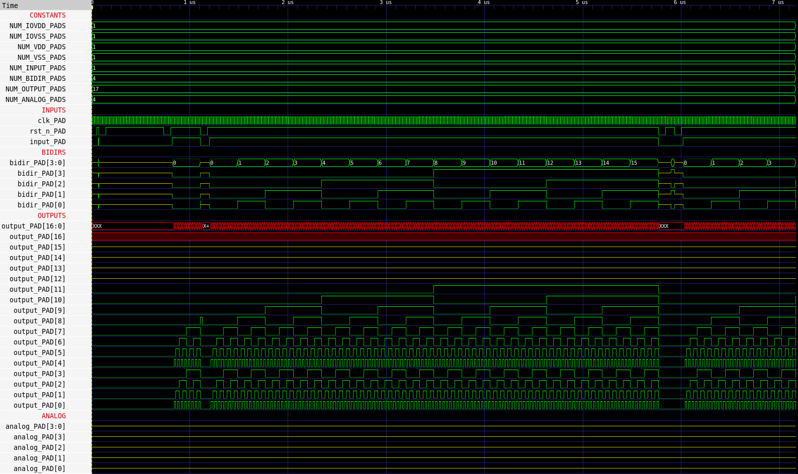
chip_top cocotb waveform in GTKWave.
For mixed-signal simulation, the testbenches/xschem/chip_top_tb_tran.sch testbench can be opened in Xschem for interactive simulation, the same way as for the counter or the inverter, and is shown in Figure 26.
cd testbenches/xschem
xschem chip_top_tb_tran.sch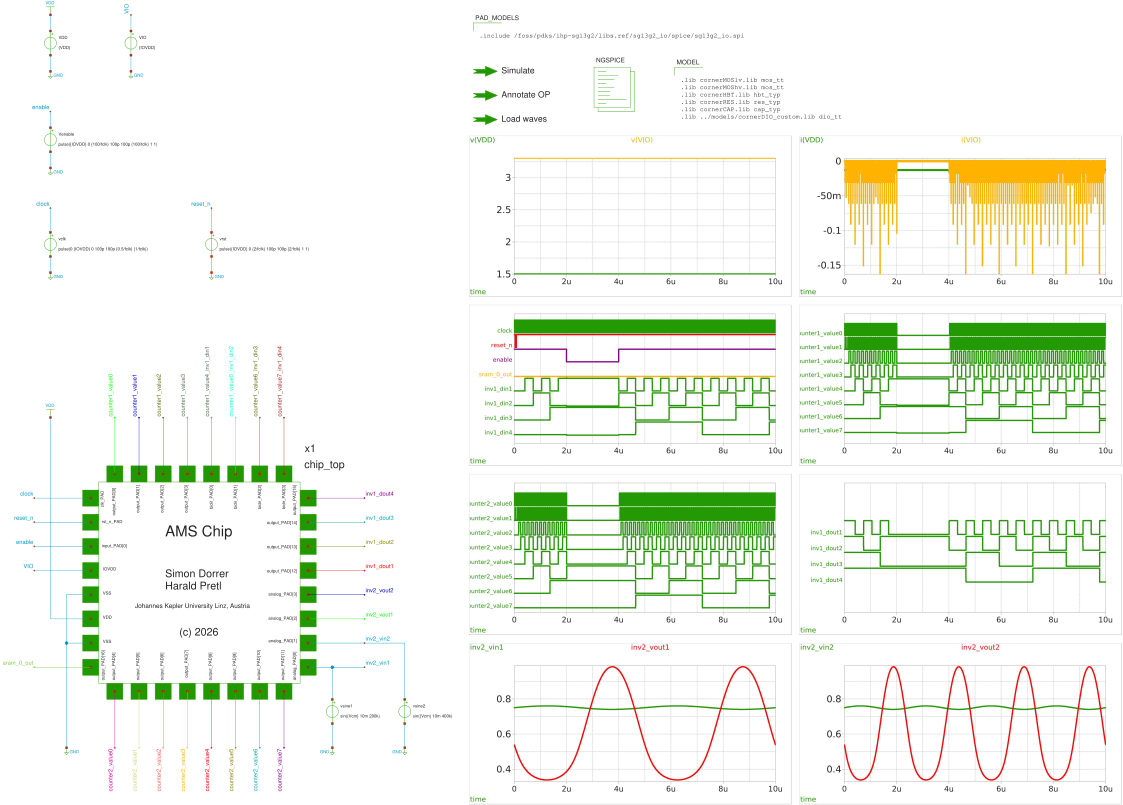
chip_top_tb_tran.
Again, the simulation and plotting can be run non-interactive from the command line with the following targets.
make sim-gl-xschem
make plot-xschem-sim TESTBENCH=chip_top_tb_tranThe top-level Xschem testbench converges, but it may take a long time depending on the hardware used. make sim-gl-xschem is therefore not part of sim-all and must be called manually when needed. For this tutorial, the simulation data is already available in the repository in scripts/plot_simulations/data/chip_top_tb_tran.txt, so make plot-xschem-sim TESTBENCH=chip_top_tb_tran can be run without running the simulation first.
The following plots show the results of the top-level transient simulation. The first plot shows the analog inverter response, while the other three plots show the digital outputs of the two counters, the digital inverter, and the bidirs.
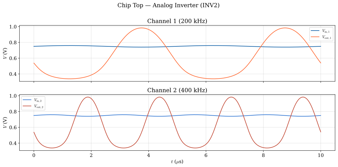
chip_top_tb_tran — analog inverter 1 response.
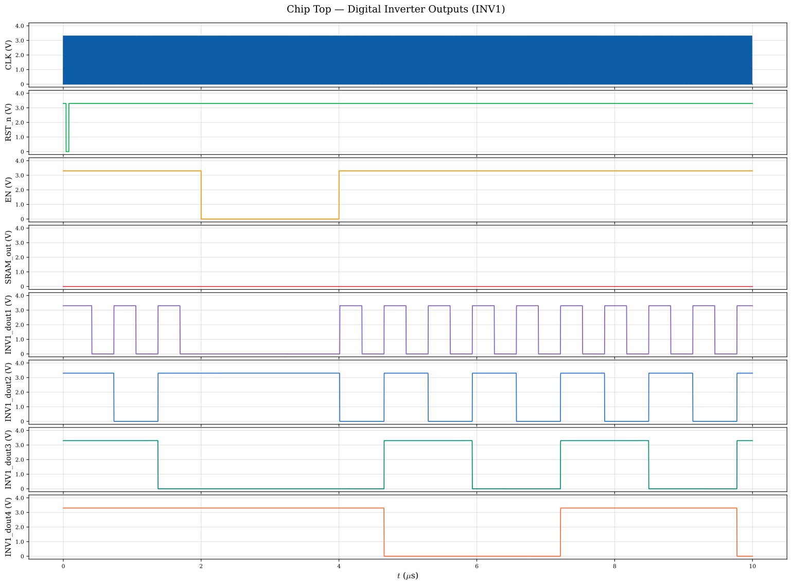
chip_top_tb_tran — digital inverter 2 outputs.
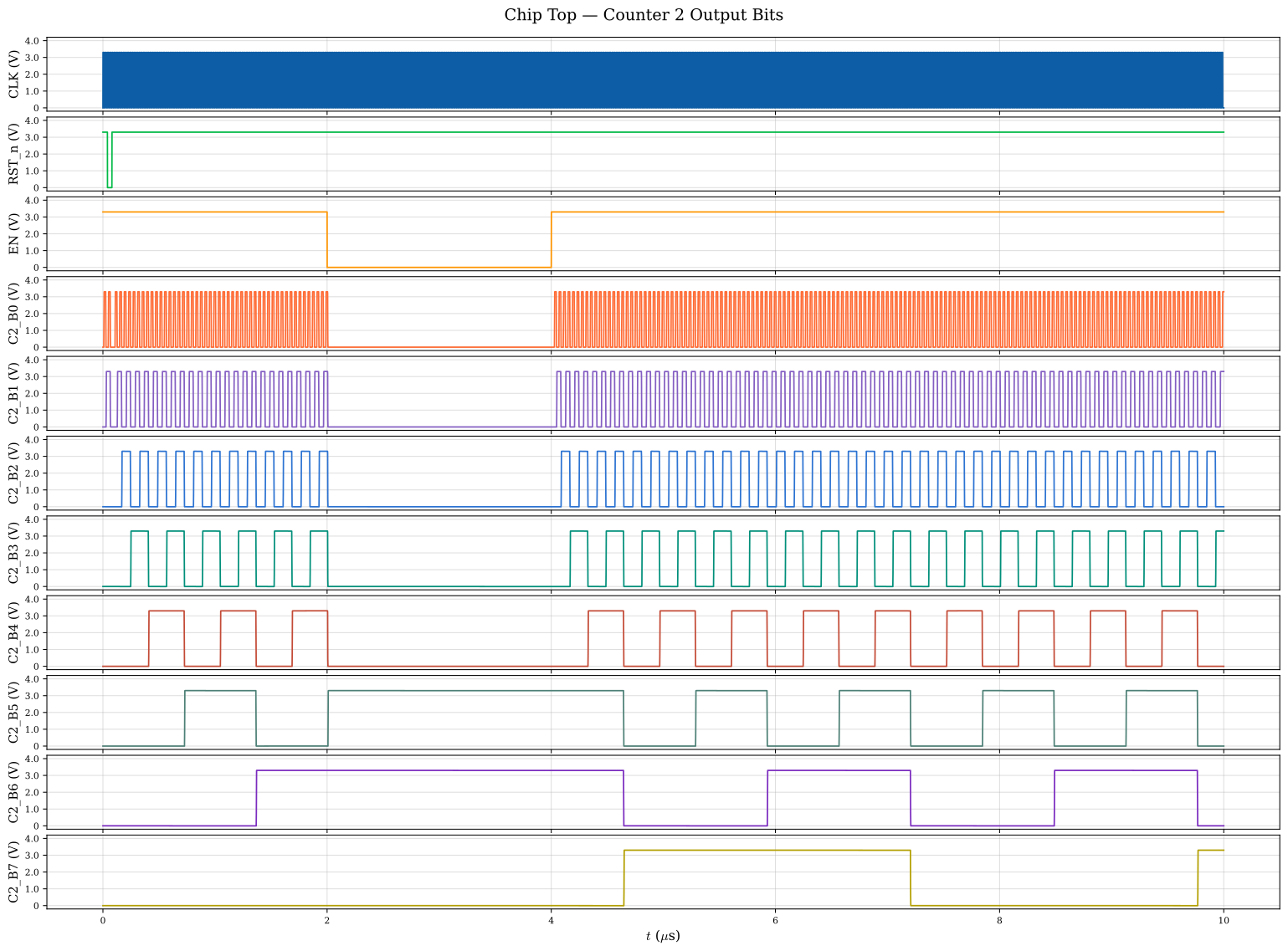
chip_top_tb_tran — digital counter 2 outputs.
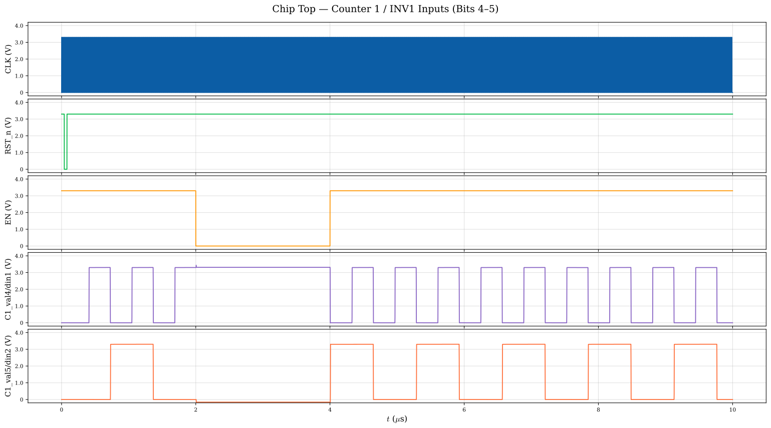
chip_top_tb_tran — digital counter 1 / inverter 1 bidirs.
When the testbench is opened in Xschem, the schematic of chip_top can be inspected with the shortcuts e / Ctrl + e, and the symbol can be shown with i / Ctrl + i as explained in Section 5. The schematic and symbol are shown in Figure 31 and Figure 32, respectively. The schematic shows the connections between the padframe and the core macros, while the symbol shows the pinout of the chip. The SRAM is not included in the schematic, since IHP does not ship a SPICE model or an Xschem symbol for the RM_IHPSG13_1P_1024x32_c2_bm_bist macro.
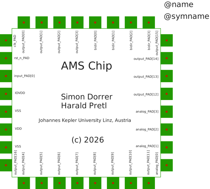
chip_top, showing the pinout of the chip.
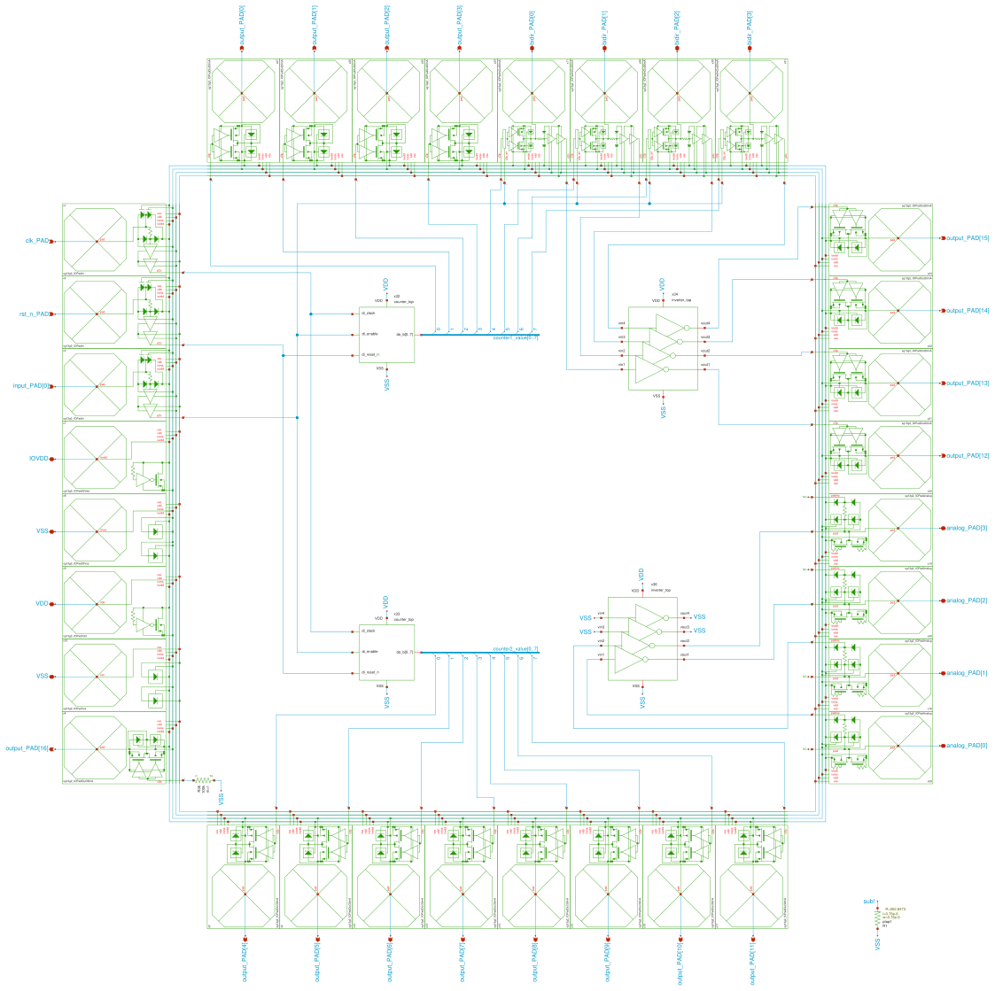
chip_top, showing the connections between the padframe and the core macros.
7.6 Building the Chip
When the floorplan and pinout are planned and configured, the chip can be built from scratch with the following command.
make build-allThis runs the steps in order, init-submodules, build-bondpad, build-logos, build-macros, and build-top. It is the right starting point on a fresh machine after cloning the repository and entering the IIC-OSIC-TOOLS container.
To re-run only the top-level flow (for example after a change in config.yaml or chip_core.sv), without rebuilding the bondpad, logos, or macros, run the following command.
make build-topInternally, build-top runs librelane-nodrc, copy-reports, copy-gds, copy-netlist, copy-render, add-logo-fill, and render-gds. The final GDS is written to layout/chip_top_logo_fill.gds.gz.
The render generated by lay2img.py, which is executed during the render-gds step, is located in render/img/. The verification reports (Yosys, antenna, STA, IR-drop, LVS, manufacturability) from the top-level LibreLane flow can be found in verification/reports/. The netlists are located in netlist/.
Note that currently the LibreLane flow streams out the top-level GDS layout/chip_top.gds.gz without the logos and the fill structures. To add the chip logo (PNG → GDS) and the fill structures on top of the LibreLane output, run:
make add-logo-fillThis calls scripts/add_logo_fill.sh and writes layout/chip_top_logo_fill.gds.gz. This step is already called by make build-top. In the future, it is planned to replace this script and Makefile target with a custom LibreLane step.
The difference between chip_top.gds.gz and chip_top_logo_fill.gds.gz is that the former is the raw top-level layout without any logos or filler cells, while the latter includes the logos and filler cells added for manufacturability and cosmetic purposes. For visual debugging in KLayout, it is recommended to use chip_top.gds.gz to avoid the visual clutter of the logos and filler, while for DRC and LVS, chip_top_logo_fill.gds.gz should be used since it is the actual layout that will be taped out.
7.7 Viewing the Chip
After a successful build, the chip can be opened with KLayout.
ke layout/chip_top.gds.gz             # Chip layout without logos and filler
ke layout/chip_top_logo_fill.gds.gz   # Chip layout with logos and filler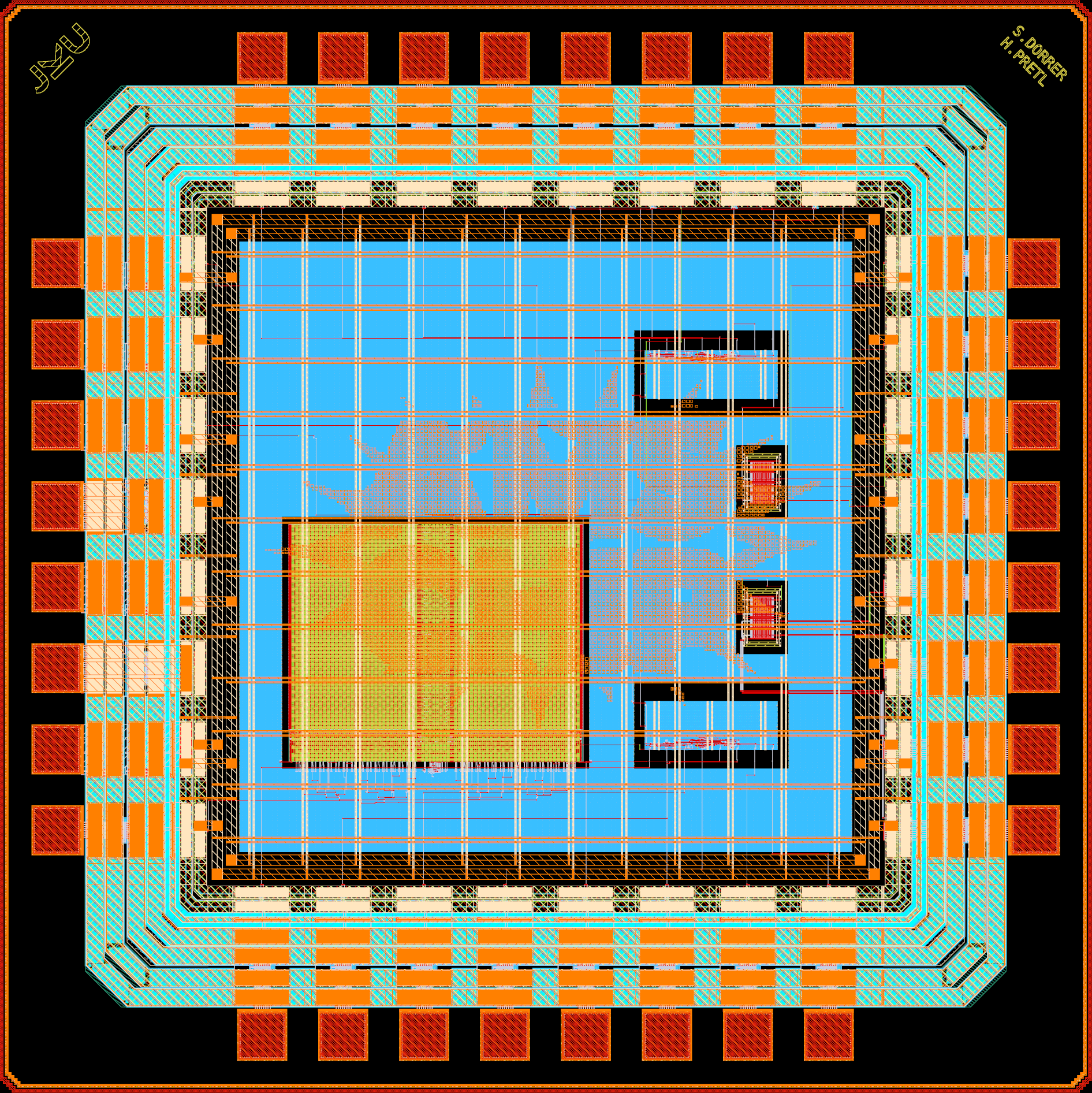
chip_top_logo_fill layout in KLayout (“all” layers).
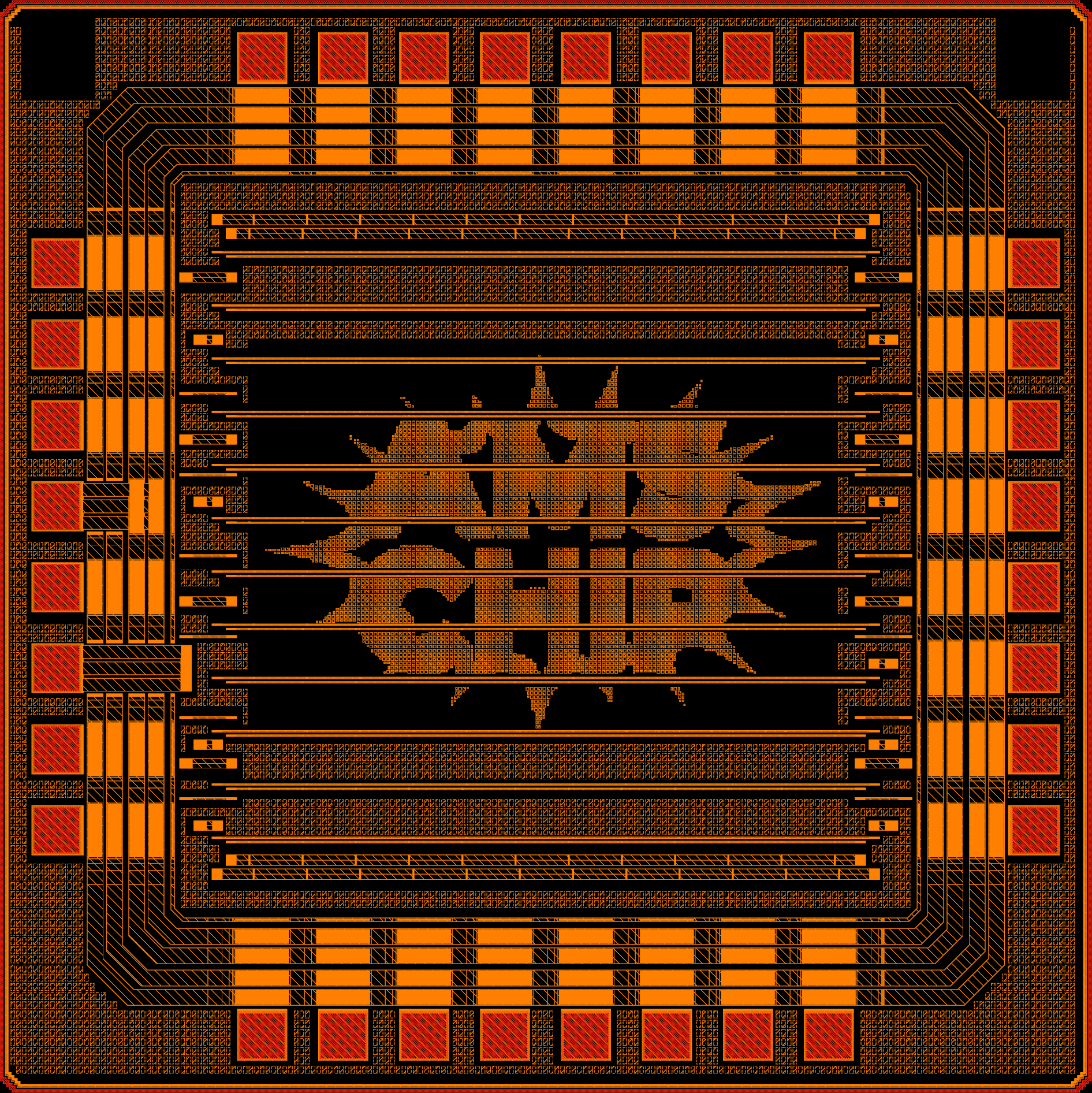
chip_top_logo_fill layout in KLayout with only TopMetal2 selected.
7.8 Chip-Level Verification
DRC, LVS, and PEX are also available for the full chip.
7.8.1 DRC
The following DRC targets are available for the top-level.
make magic-drc CELL=chip_top              # Magic DRC on the bare chip
make magic-drc CELL=chip_top_logo_fill    # Magic DRC including logo + filler
make klayout-drc-minimum                  # fast pre-check KLayout DRC on chip_top_logo_fill.gds.gz
make klayout-drc-regular                  # full KLayout DRC on chip_top_logo_fill.gds.gz (slower)
klayout-drc-minimum is a quick pre-check on the final top-level layout including the logo and the fill structures. klayout-drc-regular does the full check, but takes longer. magic-drc is faster than klayout-drc, but it does not support the full set of DRC rules and is less accurate on the complex top-level layout, so it is recommended to use both.
7.8.2 PEX
The following PEX target is available for the top-level.
make magic-pex # only chip_top (without logo and filler), default EXT_MODE=1At the top level, PEX is only run on chip_top (without logo and filler), and the default EXT_MODE=1 (C-decoupled) is used to keep the runtime manageable. However, the extracted netlist chip_top_magic_pex_1.spice is still huge (~75 MB, ~566k lines), and the post-layout simulation must be run on a powerful server.
7.8.3 LVS
The following LVS target is available for the top-level.
make klayout-lvs                          # top-level KLayout LVS
make magic-lvs # top-level Magic + Netgen LVSThe top-level LVS is currently under construction. The flow is in place, but some issues and limitations in the ihp-sg13g2 PDK must be fixed before it can run successfully.
7.9 Packaging
The die is packaged in a QFN-32 (5x5 mm) open-molded plastic package (OmPP) from the EUROPRACTICE ASIC packaging offering. The package matches the padframe exactly: all 32 bondpads (8 per side, see Section 7) are wired one-to-one to the 32 package leads (8 per side). Bonding is done with 25 µm gold wire, the longest wire measures 1.70 mm, and the cover is glued on after bonding.
The bonding diagram below is generated fully automatically with make bondplan from the final chip GDS (layout/chip_top_logo_fill.gds.gz) and the EUROPRACTICE package library EP_PACKAGES_08022018.gds. The flow extracts the die bondpads together with their names, places the die in the package cavity, draws the bondwires, fills in the title block, and checks wire lengths, crossings, spacing, lead skew, and the clearance around the sensitive analog wires. The pinout and all flow settings are kept in a single configuration file, so the diagram never goes out of sync with the chip. Details are documented in the packaging README.
make bondplan                        # uses the default VERSION (1.0.0)
make bondplan VERSION=2.1.0          # stamp another version on the sheet
The VERSION variable is passed to the flow and printed in the title block (DIE: CHIP_TOP - V.1.0.0), so the version number is maintained in the Makefile only. The outputs are the bondplan GDS (packaging/layout/chip_top_bondplan.gds), the bond report with summary and bond table (packaging/result.md), and the bonding diagram images (packaging/render/chip_top_bondplan_{white,black}.{png,svg}).
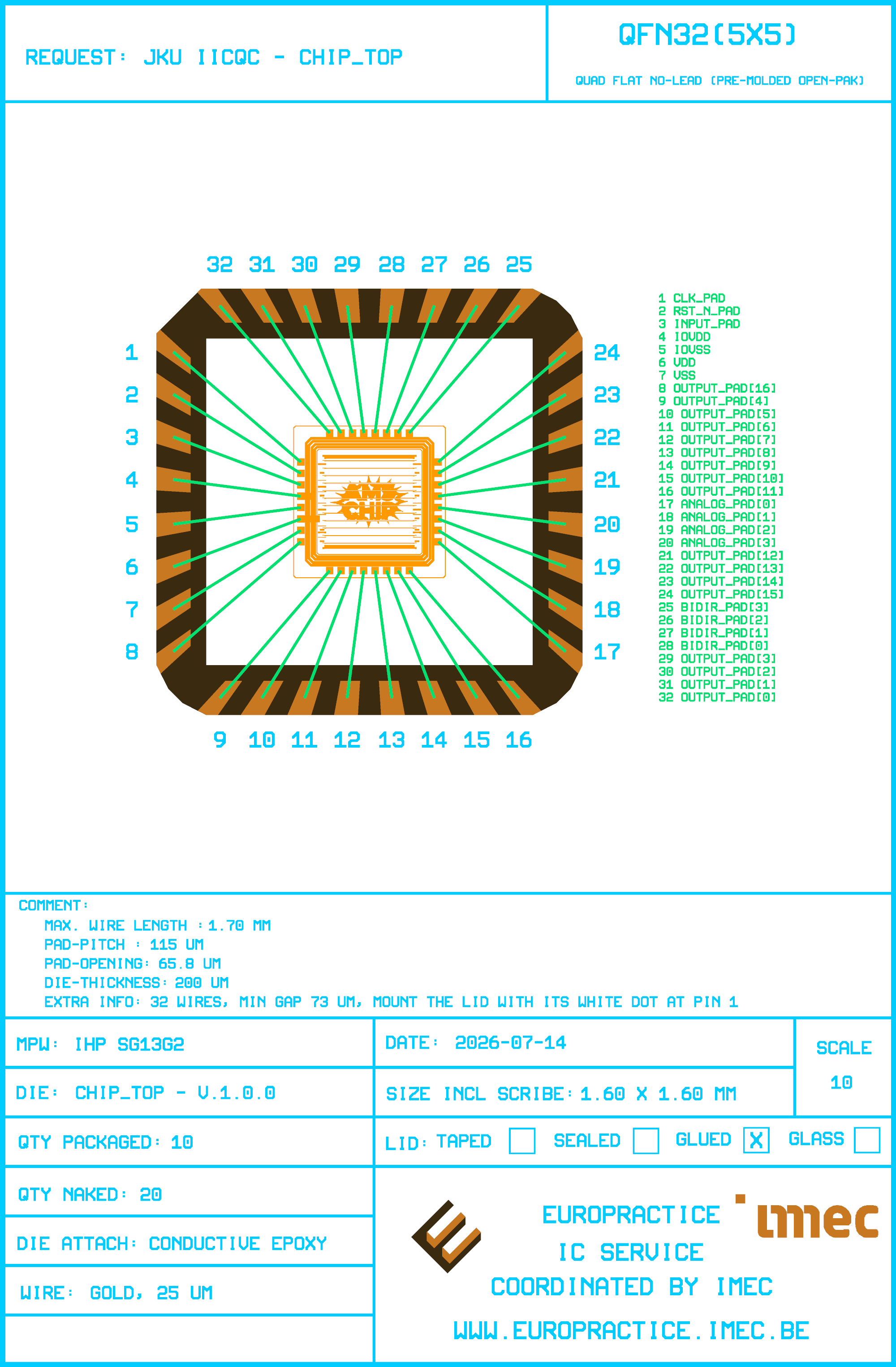
Check the flow log and packaging/result.md after every run. Unbonded named pads and NC package pins are reported explicitly, so a forgotten connection in the PINOUT table is immediately visible. Warnings are raised for bondwires that are too long (BONDWIRE_MAX_LENGTH), cross each other, come too close to each other, land skewed on their lead (BONDWIRE_MAX_SKEW), or violate the guard clearance of sensitive wires (GUARDED_PINS / GUARD_SPACING).
7.10 Full Flow at Once
The comprehensive simulation, build, and DRC pass for the complete chip is run with the following command.
make allThis calls sim-all (RTL/GL cocotb, GL Xschem when available), then build-all, then Magic DRC on both chip_top and chip_top_logo_fill. To shorten the runtime, the KLayout DRC is currently not included in make all. However, depending on the hardware used, make all can still take a while.
7.11 Releasing for Tapeout
When the chip is clean, the release target copies the GDS, the netlists, and the renders into a versioned folder for tapeout submission.
make release VERSION=2.1.0The artifacts are written to release/v.2.1.0/ (gds/, netlist/{layout,pnl,spice}/, img/).
Run make all before make release. The release target only copies files, it does not rebuild or re-verify the chip.
8 Additional Exercises
The following exercises repeat the corresponding sections of this tutorial with modifications to the design.
8.1 Exercise 1: From 8-bit Up-Counter to 16-bit Down-Counter
Repeat Section 4 for a 16-bit synchronous down-counter that wraps from 0 back to \(2^{16} - 1 = 65535\). The recommended steps are:
- Update the RTL (
counter.sv,counter_top.sv,constants.sv). Change the bitwidth and turn the increment block into a decrement, with wrap-around from 0 toCTR_MAX. - Update the testbenches in
testbenches/verilog/,testbenches/cocotb/, andtestbenches/xschem/to cover the new behaviour. Adjust the bus width in the waveform view files (*.gtkw,*.surf.ron) as well. - Run
make sim-allto validate the new RTL. - Re-run the LibreLane flow with
make build-top. Check the timing reports. A 16-bit counter at 50 MHz must still pass timing constraints. - Regenerate the XSPICE model with
make generate-xspice, and re-run the gate-level Xschem simulation.
Replace the binary counter with a 16-bit Gray counter (only one bit toggles per transition).
8.2 Exercise 2: Self-Biased Single-Ended Inverter Amplifier
Repeat Section 5 with a self-biased single-ended inverter amplifier by adding a feedback resistor \(R_\mathrm{f}\) between the output and the input of the inverter. As discussed in Section 5.4, the bare CMOS inverter has poor PVT robustness because nothing pins the gate bias to \(V_\mathrm{DD}/2\). A feedback resistor closes a DC loop that forces the operating point to the high-gain crossover (\(V_\mathrm{in} \approx V_\mathrm{out} \approx V_\mathrm{DD}/2\)) regardless of process corner, which also linearises the small-signal transfer characteristic and turns the inverter into a usable single-ended amplifier. The disadvantage of this technique is the reduced input resistance, which equals \(R_\mathrm{in} \approx 1 / (g_\mathrm{m,NMOS} + g_\mathrm{m,PMOS})\). The recommended steps are:
- Open the inverter schematic (
inverter.sch) in Xschem and add a resistor between thevinandvoutnets of the inverter. Start with a value of \(R_\mathrm{f} \geq 10\,\mathrm{k\Omega}\) and adjust as needed. What can you observe? - Re-run the schematic-level testbenches from Section 5 and observe the change in behaviour. First, always carefully think about what the expected behaviour would be before running the simulations, and then check if the results match your expectations.
- Re-run the full schematic-level simulation suite with
make sim-allto refresh the plotted results infig/inverter_top/. - Re-run the CACE flow with
make sim-caceand compare the new process and mismatch plots against Figure 17 and Figure 19. The spread of \(A_\mathrm{ol}\) across corners should be visibly narrower than the open-loop reference. - [Optional] Sweep \(R_\mathrm{f}\) in the CACE characterisation YAML (
inverter.yaml) to study the circuit behaviour across a range of feedback resistor values. - [Optional] Once the schematic results are convincing, propagate the resistor to the layout in
layout/and re-run the verification chain (make klayout-verify,make magic-verify) plusmake build-top.
Choose \(R_\mathrm{f}\) carefully. Too small, and the loop loads the amplifier output and degrades the closed-loop gain. Too large, and the time constant with the input parasitic capacitance dominates, so the amplifier loses gain at the low end of the signal band. A value in the \(1\)–\(10\,\mathrm{M\Omega}\) range is a sensible starting point for this inverter sizing.
8.3 Exercise 3: Three-Stage Ring Oscillator with Output Buffer
Repeat Section 5 for a three-stage ring oscillator with an output buffer, derived from the existing quad inverter. The recommended steps are:
- Copy the inverter macro folder to a new location (for example
macros/ringosc/), and adapt the Makefile names. - Update the schematic in Xschem. Connect three inverters in a ring, and tap the output of the last stage through a buffer. The fourth inverter of the quad inverter can naturally be used as the buffer.
- Update the symbol of the macro (
schematic/xschem/inverter_top.sym) and the PEX symbol (schematic/xschem/inverter_top_pex.sym) to expose a single output net, instead ofvin1..vin4andvout1..vout4. - Update the transient testbench (
testbenches/xschem/inverter_top_tb_tran.sch) to measure the oscillation frequency. Delete testbenches that are no longer relevant. - [Optional] Adapt the CACE
inverter.yamlto characterise the oscillation frequency across PVT. - Update the layout in KLayout. The existing
inverter_top.klay.gdscan be used as a starting point, but the internal routing has to be modified to form the ring and the buffer stage. After editing, export a cleanringosc_top.gds. - Re-run the verification chain,
make klayout-verify,make magic-verify, andmake build-top.
8.4 Exercise 4: Update Pinout and Floorplan of the Top-Level
Building on Section 8.1 and Section 8.3, swap inverter2 for the ring oscillator, delete counter2, and connect the now 16-bit counter1 to the freed-up south-side pads. The recommended steps are:
- Replace
inverter2with the ring oscillator macro inchip_core.sv. - Replace three of the four analog pads with VSS pads, and connect the ring oscillator’s output to the fourth analog pad.
- Delete
counter2and rewire all eight south-side pads to the new 16-bitcounter1values. - Update the parameters of
chip_top.svso thatNUM_OUTPUT_PADS,NUM_BIDIR_PADS,NUM_ANALOG_PADS, andNUM_VSS_PADSmatch the new pin count (see Section 7). - Update the macro instantiation and wiring in
chip_core.sv. - Update the placement coordinates in the
MACROSblock ofconfig.yaml. Keep thedoc/floorplan.mdconstraints in mind, namely stay in the core, no overlaps, and respect theMetal3grid for inverter-like macros. - Update the PAD lists (
PAD_WEST,PAD_NORTH,PAD_SOUTH,PAD_EAST) inconfig.yamlto match the new pinout. - Update
pdn_cfg.tclso that the new macros are covered by the correct PDN grid (default for digital,inverter_top-style for analog). - Rebuild the chip from scratch with
make build-all, then verify withmake magic-drc CELL=chip_topandmake klayout-drc-minimum.
8.5 Exercise 5: Update the Bondplan Configuration
Building on Section 8.4, update the bondplan configuration in packaging/config.yaml so that the packaged chip matches the new pinout (ring oscillator instead of inverter2, 16-bit counter1, no counter2, three additional VSS pads). The recommended steps are:
- Rebuild the final GDS of the modified chip (
make build-allfrom Section 8.4), since the bondplan flow reads the die pads and their names directly fromlayout/chip_top_logo_fill.gds.gz. - Update the
PINOUTtable inpackaging/config.yaml: the south-side pads now carrycounter1_value[15:8], three of the four east-side analog pads became VSS pads, and the fourth carries the ring-oscillator output. Keep the geometric order in mind (pins 1-8 left top→bottom, 9-16 bottom left→right, 17-24 right bottom→top, 25-32 top right→left) so that the bondwires do not cross. - Connect the freed-up VSS pads as downbonds to the exposed pad by adding an
EPADlist (e.g.EPAD: ["VSS", "VSS", "VSS"]) and marking their former leads as NC (~). The exposed pad of the QFN32 is the package ground, and the die is attached with conductive epoxy, so ground downbonds are shorter and lower-inductance than wires to leads. - Re-run
make bondplanand read the flow log andpackaging/result.mdcarefully: only the deliberately unbonded pads may appear as unbonded named pads (plus the seal-ring artifact), and there must be no wire-length, crossing, spacing, lead-skew, or guard-clearance warnings. - Inspect the generated bonding diagram in
packaging/render/and the bondplan GDS in KLayout (ke packaging/layout/chip_top_bondplan.gds). The title block of the A4 drawing sheet (die size, pad pitch, wire count, maximum wire length) is refilled automatically on every run. - [Optional] Experiment with the die placement: rotate the die with
DIE_PLACEMENT.orientation(e.g.E) or move it off-center withDIE_PLACEMENT.location, re-run the flow, and observe how the wire-length, spacing, and skew checks react. Restore a placement where all checks pass.
9 RFIC Flow
Are you interested in an open-source RFIC flow? Check it out here.
10 Acknowledgements
This project is funded by the JKU/SAL IWS Lab, a collaboration of Johannes Kepler University and Silicon Austria Labs.

|

|