

Radio-Frequency Integrated Circuits
1 Introduction
This is the material for an introductory radio-frequency integrated circuits course. The contents are largely based on (Razavi 2011; Darabi 2020); these two books are an excellent introduction to this topic and are highly recommended! For a general introduction to RF and microwave, (Pozar 2011) is a great read!
It is assumed that readers are familiar with the contents of this Analog Circuit Design course.
Important
All course material (source code of this document, Jupyter notebooks for calculations, Xschem circuits, etc.) is made publicly available on GitHub (follow this link) and shared under the Apache-2.0 license.
Please feel free to submit pull requests to fix typos or add content! If you want to discuss something that is not clear, please open an issue.
The production of this document would be impossible without these (and many more) great open-source software products: VS Code, Quarto, Pandoc, LaTeX, Typst, Jupyter Notebook, Python, Xschem, ngspice, CACE, pygmid, schemdraw, Numpy, Scipy, Matplotlib, Pandas, Git, Docker, Ubuntu, GNU/Linux, …
1.1 Wireless Transmission
In wireless transmission, we usually want to transmit data from a transmitter (TX) and its connected antenna towards a receiver (RX) using an electromagnetic (EM) wave. This arrangement is shown in Figure 1.
Unfortunately, wireless transmission is hard. The wireless channel, i.e., the usage of electromagnetic waves to transmit information from a transmitter to a receiver, while tremendously useful, has quite a few undesired features:
- The wireless channel is shared between all users.
- As a consequence, the available bandwidth is shared; this means that bandwidth is a scarce resource.
- The wireless channel has significant losses.
- The channel is time variant, as usually the transmitter and/or the receiver move, and/or the environment changes.
In order to estimate the received power \(P_\mathrm{R}\) from a wireless transmission, we can use Friis’ transmission formula (Pozar 2011):
\[ P_\mathrm{R} = \frac{P_\mathrm{T}}{4 \pi d^2} \cdot A_\mathrm{R} = P_\mathrm{T} \cdot \frac{A_\mathrm{R} \cdot A_\mathrm{T}}{d^2 \lambda^2} \tag{1}\]
Here, \(A_\mathrm{R}\)/\(A_\mathrm{T}\) is the effective area of the receive/transmit antenna, while \(d\) is the distance (line of sight) between the two antennas, and \(\lambda\) is the wavelength of the EM wave. The effective area of an antenna depends on the type and construction, but generally we can say that
\[ A \propto \lambda^2 \]
For an isotropic antenna (a theoretical construct where the radiation is of equal strength in all directions) \(A = \lambda^2 / (4 \pi)\), while for a \(\lambda/2\)-dipole \(A = 0.13 \lambda^2\). Of course, the speed of light \(c = 3 \times 10^{8}\,\text{m/s}\) relates frequency \(f\) and the wavelength \(\lambda\) of an electromagnetic wave by
\[ c = \lambda f. \]
Generally speaking, the size of an electromagnetic antenna is proportional to the wavelength of the EM wave used for transmission. For many devices, we seek antennas with dimensions on the order of a few centimeters, and this is why frequencies in the hundreds of MHz to GHz are so popular. Table 1 lists a few typical applications and their frequencies and wavelengths.
| Application | Frequency | Wavelength |
|---|---|---|
| FM Radio | 88 MHz to 108 MHz | 3.4 m down to 2.8 m |
| WiFi (lowband) | 2.4 GHz | 12.5 cm |
| WiFi (highband) | 5 GHz | 6 cm |
| Bluetooth | 2.4 GHz | 12.5 cm |
| Cellular | 0.6 GHz to 5 GHz | 50 cm down to 6 cm |
| GNSS | 1.575 GHz | 19 cm |
As you can see in Table 1, many of these antennas would not fit into typical device form factors, i.e., often we have to use electrically small antennas. As antenna design is not part of this course but critically important for wireless systems, please refer to (Balanis 2005) or this website for more information on antenna design.
Note 1: Wavelength Calculation
Let’s calculate the wavelength for a Bluetooth signal at 2.4 GHz. Given:
- Frequency \(f = 2.4\,\text{GHz} = 2.4 \times 10^9\,\text{Hz}\)
- Speed of light \(c = 3 \times 10^8\,\text{m/s}\)
Using the relationship \(c = \lambda f\), we can solve for wavelength:
\[\lambda = \frac{c}{f} = \frac{3 \times 10^8\,\text{m/s}}{2.4 \times 10^9\,\text{Hz}} = 0.125\,\text{m} = 12.5\,\text{cm}\]
This means that a quarter-wavelength monopole antenna for 2.4 GHz Bluetooth would be approximately 3.1 cm long, which easily fits into most mobile devices.
In order to get a feeling for the attenuation experienced in wireless communication, we now calculate the following example transmission. We will use the unit of dBm which is often used in RF design and is defined as
\[ P|_\text{dBm} = 10 \cdot \log_{10} \left( \frac{P|_\text{W}}{1\,\text{mW}} \right) \tag{2}\]
which is a logarithmic measure of power relative to 1 milliwatt. For example, 1 W = 30 dBm, 100 mW = 20 dBm, and 1 mW = 0 dBm.
Note 2: Wireless Transmission
We use the following parameters:
- Transmit power \(P_\mathrm{T} = 1\,\text{W}\)
- Frequency \(f = 2.4\,\text{GHz}\)
- Communication distance \(d = 10\,\text{km}\)
- Using \(\lambda/2\) dipoles on both ends
Using Equation 1 we calculate
\[ P_\mathrm{R} = P_\mathrm{T} \cdot \frac{0.13 \lambda^2 \cdot 0.13 \lambda^2}{d^2 \lambda^2} = P_\mathrm{T} \cdot 0.13^2 \left( \frac{\lambda}{d} \right)^2 = 2.64\,\text{pW} = -85.8\,\text{dBm} \]
With the transmit power of 1 W = 30 dBm we have an attenuation of 116 dB! This is a very large number!
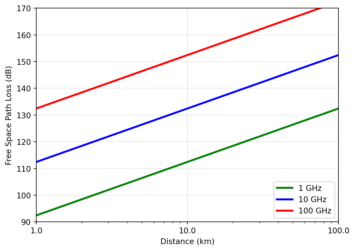
The loss we calculated in Note 2 is called the free-space path loss (FSPL). It is the minimum loss we can expect in a wireless communication system. In reality, the situation is often even worse. The FSPL (in dB) can be calculated as
\[ \text{FSPL} = 20 \cdot \log_{10}(d / \text{m}) + 20 \cdot \log_{10}(f / \text{Hz}) + 20 \cdot \log_{10} \left( \frac{4\pi}{c} \text{m/s} \right). \tag{3}\]
Equation 3 can be readily derived from Equation 1 and Equation 2 assuming isotropic antennas at transmitter and receiver. Using Equation 3 we can calculate the FSPL for different distances \(d\) and frequencies \(f\). The results are shown in Figure 2. It should be noted that the FSPL increases by 20 dB per decade of distance and 20 dB per decade of frequency, making the use of higher frequencies and longer distances very challenging.
As dire as the situation of Figure 2 already looks, these are not even all the factors to consider:
- The given attenuation is for line-of-sight paths; often, the attenuation is significantly higher than this due to blockage by buildings, mountains, rain, or foliage.
- In the absence of a direct line-of-sight path, the EM wave is redirected by reflections, causing additional attenuation and potential destructive interference due to multi-path reception.
The consequences of this are (among others):
- The transmitter needs to generate enough transmit power to overcome the transmission loss; this has to be done with high efficiency, as the transmit device is battery operated or limited by cooling.
- The receiver has to be able to process weak signals, i.e., the noise level of the signal processing has to be very low.
- Often, the receive signal is very weak, while there are strong signals at other frequencies (i.e., other wireless transmitters are located close to the receiver). This means the receiver has to be able to process a weak signal while simultaneously tolerating large interfering signals (called blockers).
- Since the frequency spectrum is shared among many users and wireless applications, the transmit information has to be packed efficiently into a small bandwidth.
- Very often, wireless devices are battery-operated. This means transmit and receive functions have to be implemented using minimum power consumption.
As stated in the beginning, designing wireless systems is hard.
1.2 Wireless Standards
In order to allow communication between different devices, different operators, and different manufacturers, wireless communication is usually standardized. There are many different standards, each with its own characteristics. Wireless standards define every aspect of wireless communication, and can be documents of hundreds or thousands of pages. Here, we mainly focus on the radio-frequency and analog aspects of wireless standards. Summarized in Table 2 are a few popular wireless standards with their main characteristics.
| Standard | GSM (2G) | WCDMA (3G) | LTE (4G) 5G NR |
WiFi | Bluetooth | GNSS |
|---|---|---|---|---|---|---|
| Frequency range (MHz) | 850, 900, 1800, 1900 | 850, 900, 1700, 1900, 2100 | Multiple bands 450…7100 (FR1), 24000…48000 (FR2) | 2400, 5000, 6000 | 2400 | 1500, 1200 |
| Modulation | GMSK, 8PSK (EDGE) | QPSK (DL), BPSK (UL), 16QAM (HSPA), 64QAM (HSPA) | QPSK, 16QAM, 64QAM (DL+UL) 256QAM (DL+UL) | BPSK, QPSK, 16QAM, 64QAM, 256QAM, 1024QAM, 4096QAM | GFSK (m=0.28…0.35), \(\pi\)/4-DQPSK, 8DPSK | BPSK, QPSK |
| Transmission/ multiple access | TDMA, FDMA | DS-CDMA | OFDMA (DL+UL), SC-FDMA/DFT-s-OFDM (UL) | OFDM, CSMA/CA | FHSS | CDMA |
| Duplex | FDD | FDD | FDD, TDD | TDD | TDD | n/a |
| Channel bandwidth | 200 kHz | 5 MHz | 1.4, 3, 5, 10, 15, 20, …, 100 MHz (FR1), 400 MHz (FR2) | 10, 20, 40, 80, 160, 320 MHz | 1 MHz | 16…24 MHz |
| Symbol rate1 | 270.833 ksym/s | 3.84 Msym/s | 15/30/60 ksym/s | 312.5 ksym/s | 1 Msym/s | 50 sym/s |
| Pulse shaping | Gaussian (BT=0.3) | Root Raised Cosine (\(\alpha\)=0.22) | Rectangular | Rectangular | Gaussian (BT=0.5) | Rectangular |
| Transmit power | 1…2 W | 250 mW | 200 mW (FDD), 400 mW (TDD) | 100 mW | 1…100 mW | n/a |
| PAR (UL) | 0 dB (GMSK), 3 dB (8PSK) | 3…8 dB | 6…8 dB | Up to 12 dB | 0 dB (GFSK), 3 dB (8DPSK) | n/a |
| MIMO | no | Not realized (DL 2x2) | DL 4x4 (up to 8x8) | 2x2 (up to 8x8) | no | no |
| Channel bond | no | Up to 4x5 MHz | Up to 7x20/4x100 MHz | Up to 80+80+80+80 MHz | no | no |
During this course, we will learn what these terms mean and how they impact the design of RF integrated circuits.
As you can see in Table 2, since LTE (4G) and 5G NR, many additional bands have been defined in the sub-6 GHz range (FR1) and also in the mm-wave range (FR2, 24.25 to 52.6 GHz). This means that modern wireless devices have to support many different frequency bands, which makes the design of RF front ends even more challenging. A good overview of the different frequency bands is given here for LTE and 5G NR.
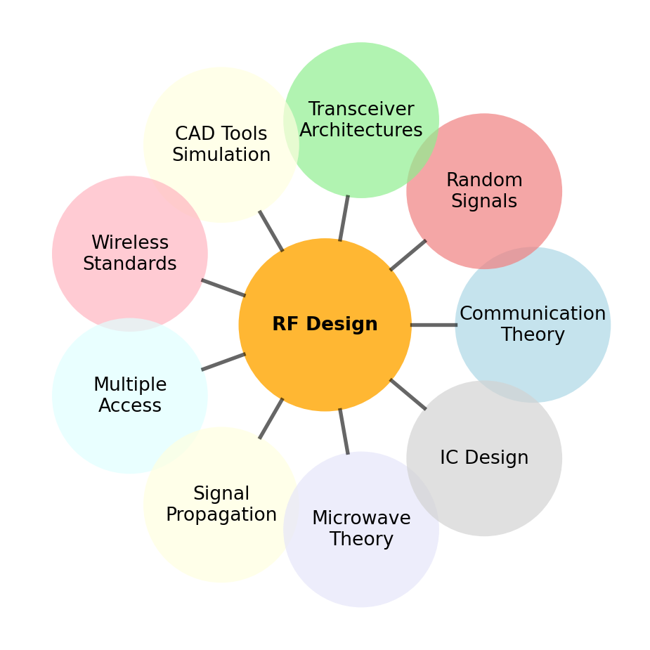
RFIC design is a multidisciplinary field, requiring knowledge from various engineering domains, as shown in Figure 3. This makes RFIC design challenging, but also very interesting!
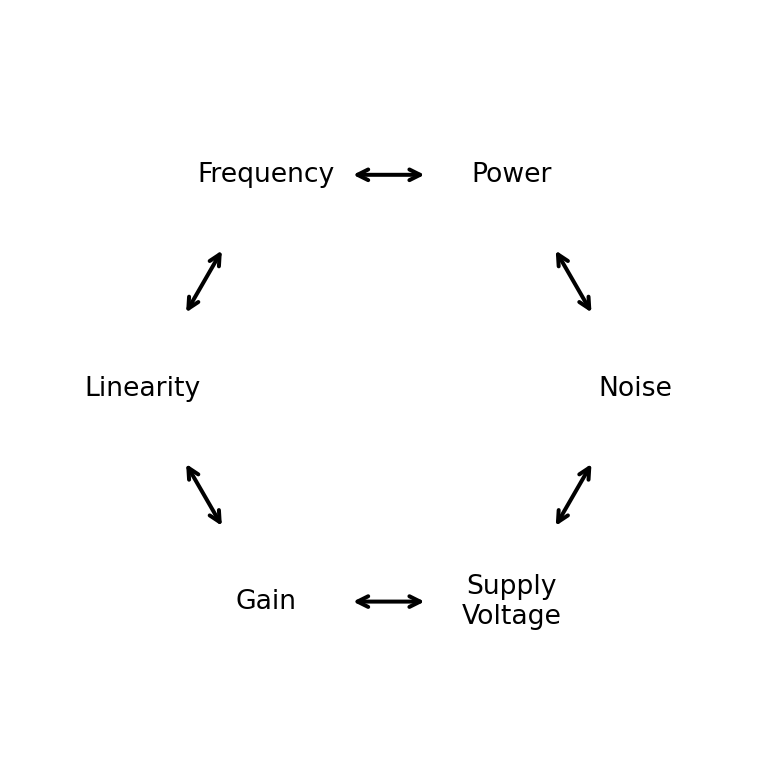
Further, RFIC design requires careful consideration of many different aspects, as shown in Figure 4. Many parameters are often tightly coupled, requiring careful trade-offs during the design process.
2 Fundamentals
In this section, we will discuss a few important concepts which will be instrumental in the further study of RF circuits and systems. As the dynamic range of signals in RF circuits and systems is often limited on the top end by linearity, and on the bottom end by noise, we will discuss these two topics in some detail.
2.1 Channel Capacity
In Section 1 we have already discussed the fact that we need to pack information into a minimum bandwidth, as the available spectrum is limited. To appreciate the limits of information transfer, we need to understand how much information can be transmitted over a given bandwidth. This limit is given by the Shannon-Hartley theorem, which states the maximum data rate \(C\) (in bit/s) that can be transmitted over a communication channel with bandwidth \(B\) (in Hz) and signal-to-noise ratio \(\text{SNR}\) (in linear units):
\[ C = B \cdot \log_2(1 + \text{SNR}) \tag{4}\]
This formula provides us a theoretical upper limit on the data rate that can be achieved with a given bandwidth and SNR under optimal conditions. It is important to note that this limit is only achievable with ideal coding and modulation schemes, which are not practical in real-world systems. However, it provides a useful benchmark for evaluating the performance of communication systems.
Note 3: Channel Capacity Example
Let us calculate the channel capacity for a system with an RF bandwidth of 2 MHz and an SNR of 7 dB (the BW and minimum SNR of Bluetooth LE for 1 Mbps). First, we need to convert the SNR from dB to linear units:
\[ \text{SNR} = 10^{{7}/{10}} \approx 5 \]
Now we can use Equation 4 to calculate the channel capacity:
\[ C = B \cdot \log_2(1 + \text{SNR}) = 2\,\text{MHz} \cdot \log_2(1 + 5) = 2\,\text{MHz} \cdot 2.585 \approx 5.2\,\text{Mbps} \]
This sounds reasonable, as the user data rate for Bluetooth LE is 1 Mbps for the given SNR, which allows for considerable overhead for coding and protocols.
2.2 Linearity
As we have already seen in Section 1.1, the transmitter has to process large signals without distorting them, while the receiver has to process small signals in the presence of large signals. Both situations mean we need metrics and models to quantify and discuss linearity properties.
We are going to use a very simple, time-invariant model to study linearity, based on a Taylor polynomial.
ImportantLinearity and Memoryless Systems
We use a memoryless (also called “instantaneous”) nonlinear model to simplify the mathematics. A memoryless nonlinear system has the property that the output at time \(t\) only depends on the input at time \(t\).
In contrast, a system with memory will have an output at time \(t\) which depends on the input at time \(t\) and also on past inputs (e.g., at times \(t - \Delta T, t - 2 \Delta T, \ldots, t - N \Delta T\)). Such a system can additionally be time-variant, which means its behavior changes over time, which leads to quite a few very interesting and important phenomena! Examples of systems with memory are filters, which have a frequency-dependent response, or power amplifiers with thermal memory effects.
We model a nonlinear circuit block with the input \(x(t)\) and the output \(y(t)\) with the following Taylor polynomial:
\[ \begin{split} y(t) &= \alpha_0 + \alpha_1 x(t) + \alpha_2 x(t)^2 + \alpha_3 x(t)^3\\ & + \alpha_4 x(t)^4 + \alpha_5 x(t)^5 + \ldots \end{split} \tag{5}\]
Usually, the blocks under study will have higher-order nonlinear terms, but we often stop at 5th order to keep things simple. For practical work, higher-order terms should be included if necessary.
Which \(x(t)\) should we use to study wireless systems? Often, the bandwidth \(\Delta f_\mathrm{BW}\) of a transmit signal is much smaller than the center frequency \(f_0\), i.e., \(\Delta f_\mathrm{BW} \ll f_0\). In this case, using a sinusoidal signal as a model is both simple to handle and approximately correct.
2.2.1 Single-Tone Linearity
We thus use (with \(A_0\) being the amplitude of the input signal and \(\omega_0 = 2 \pi f_0\) the angular frequency)
\[ x(t) = A_0 \cos(\omega_0 t) \]
and insert it into Equation 5. After some simple trigonometric manipulations we arrive at
\[ \begin{split} y(t) & = \underbrace{\alpha_0 + \frac{1}{2} \alpha_2 A_0^2 + \frac{3}{8} \alpha_4 A_0^4}_{\text{dc component }(\omega=0)}\\ & + \underbrace{\left( \alpha_1 A_0 + \frac{3}{4} \alpha_3 A_0^3 + \frac{5}{8} \alpha_5 A_0^5 \right) \cos(\omega_0 t)}_{\text{fundamental }(\omega_0)}\\ & + \underbrace{\left( \frac{1}{2} \alpha_2 A_0^2 + \frac{1}{2} \alpha_4 A_0^4 \right) \cos(2 \omega_0 t)}_{\text{2nd harmonic }(2 \omega_0)}\\ & + \underbrace{\left( \frac{1}{4} \alpha_3 A_0^3 + \frac{5}{16} \alpha_5 A_0^5 \right) \cos(3 \omega_0 t)}_{\text{3rd harmonic }(3 \omega_0)}\\ & + \underbrace{\frac{1}{8} \alpha_4 A_0^4 \cos(4 \omega_0 t)}_{\text{4th harmonic }(4 \omega_0)}\\ & + \underbrace{\frac{1}{16} \alpha_5 A_0^5 \cos(5 \omega_0 t)}_{\text{5th harmonic }(5 \omega_0)} + \ldots \end{split} \tag{6}\]
The gain \(H^{\omega_0}\) of the fundamental tone at \(\omega_0\) would be
\[ \begin{equation} H^{\omega_0} = \frac{y^{\omega_0}}{x^{\omega_0}} = \alpha_1 + \frac{3}{4} \alpha_3 A_0^2 + \frac{5}{8} \alpha_5 A_0^4. \end{equation} \tag{7}\]
Looking at Equation 6 and Equation 7, we can make a few interesting observations:
- Even-order nonlinearities (due to \(\alpha_2\) and \(\alpha_4\)) create low-frequency components; they effectively add frequency components stemming from the envelope \(A_0\). If \(A_0\) is a constant then this results in a dc term; if \(A_0(t)\) is time-variant, it will create a squared and quadrupled version of it at low frequencies.
- The \(\alpha_1\)-term is the gain of the circuit block.
- Odd-order nonlinearities (\(\alpha_3\) and \(\alpha_5\)) can impact the gain of the fundamental term passing through the block. Often \(\alpha_3\) and \(\alpha_5\) have the same sign, which is opposite to the sign of \(\alpha_1\). This implies that the gain stays linear for small input powers. For larger input signals, the terms with \(\alpha_3\) and \(\alpha_5\) start to dominate, leading to gain compression or saturation effects, until the circuit block reaches a level of maximum output power. In some cases, \(\alpha_3\) has the same sign as \(\alpha_1\) but \(\alpha_5\) has the opposite one, which leads to gain expansion: The gain would first demonstrate an overshoot at some input power level, until the term with \(\alpha_5\) becomes dominant and the gain is compressed again.
- Even- and odd-order nonlinearities create additional frequency components, so-called harmonics of the fundamental frequency. These harmonics are often unwanted, as they are far outside the wanted transmission frequency range, and need to be minimized, by either
- using a lowpass to filter these harmonics, or
- increasing the linearity, i.e., making the \(\alpha_2\), \(\alpha_3\), etc., small enough.
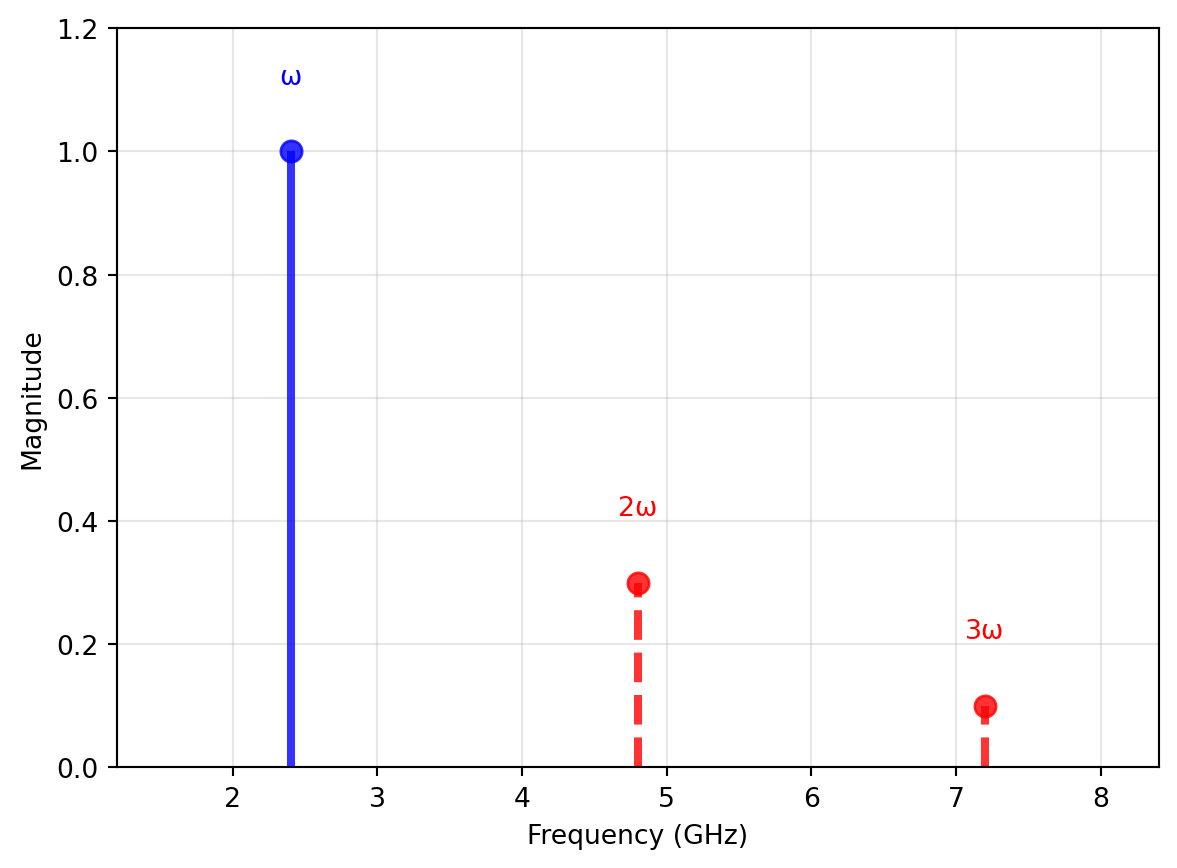
The created harmonics are illustrated in Figure 5. Note that measuring harmonics to quantify the nonlinearity metrics like \(\alpha_2\) and \(\alpha_3\) is often not very accurate, as these harmonics are often filtered in bandwidth-limited systems.
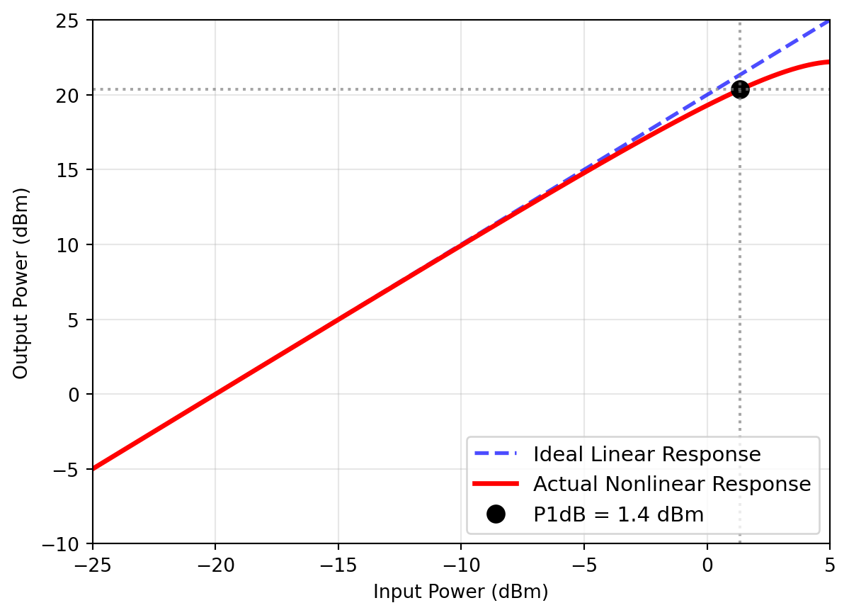
How can we quantify the nonlinearity with a one-tone test? We can sweep the input signal \(x(t)\) in amplitude, and observe the output \(y(t)\). If the observed gain drops by 1 dB from the small-signal value, we note the input power and call this point the 1 dB compression point (\(P_\mathrm{1dB}\)). We should always add whether this 1-dB compression point is input- or output-referred to avoid ambiguity. The diagram in Figure 6 shows this test (\(\alpha_1 = 100\), \(\alpha_3 = -0.2\)).
ImportantCompressive vs. Expansive Behavior
Note that for compressive behavior, \(\alpha_3\) and \(\alpha_1\) have different signs, while for expansive behavior, they have the same sign.
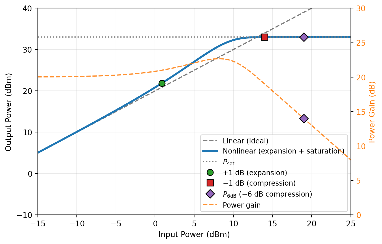
The following plot (Figure 7) in addition shows an expansive behavior. In contrast to the truncated Taylor-series model above, a closed-form saturating model is used here so that the output power correctly converges to the saturation power \(P_\mathrm{sat}\) for large input levels. Such saturating amplitude models are widely used to describe power-amplifier nonlinearity (Saleh 1981). The model uses the amplitude characteristic
\[ A_\mathrm{out} = A_\mathrm{sat} \tanh \left( u + c \cdot u^3 \right) \]
with the normalised amplitude \(u = \sqrt{G_0 P_\mathrm{in} / P_\mathrm{sat}}\) and an expansion coefficient \(c > 1/3\). At small input powers the gain equals the small-signal gain \(G_0\); at intermediate powers the gain expands above \(G_0\) (because the cubic term in the argument of \(\tanh(\cdot)\) adds extra gain before the saturation takes effect); and at large input powers the output saturates at \(P_\mathrm{sat}\) while the gain drops steeply. This (partly) expansive behavior can be used to linearize the gain of a circuit block over a wider input power range, which is often desirable in RF power amplifiers (see Section 8.2).
2.2.2 Multi-Tone Linearity
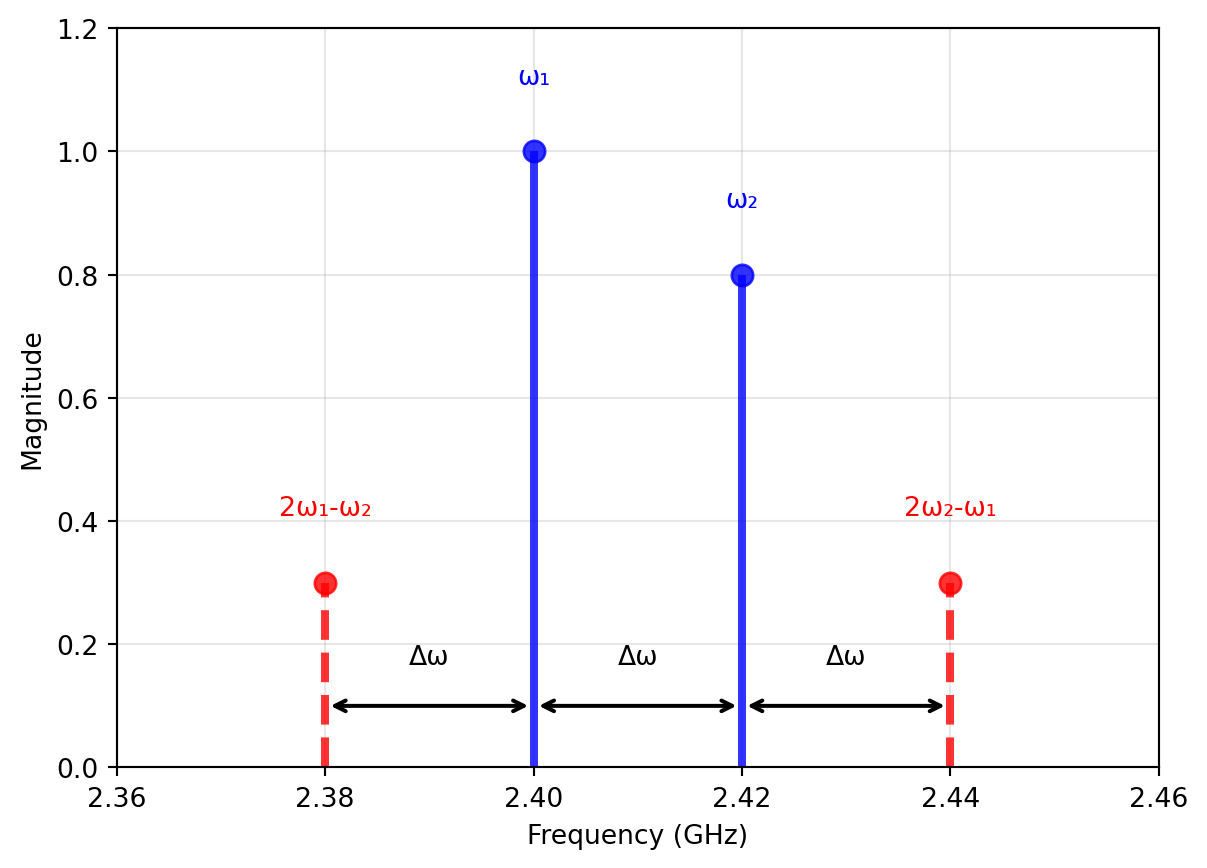
We now extend our investigations and apply two sinusoids with different frequencies \(\omega_1\) and \(\omega_2\) and different amplitudes \(A_1\) and \(A_2\) and see which signals we get at the output of the nonlinear block. The two-tone test and resulting third-order intermodulation products (IM3) are illustrated in Figure 8.
\[ x(t) = A_1 \cos(\omega_1 t) + A_2 \cos(\omega_2 t) \]
We apply the above stimulus to our nonlinear model described by Equation 5 and again, after some trigonometric manipulations, arrive at:
\[ y(t) = y'(t) + y''(t) + y'''(t) \tag{8}\]
As many different frequency components are created by this simple two-tone test (and nonlinearity only up to 3rd order), we split the result into different equations and look at the result separately.
First, we start with the fundamental tones:
\[ \begin{split} y'(t) &= \left( \underbrace{\alpha_1 A_1 + \frac{3}{4} \alpha_3 A_1^3}_\text{compression/expansion} + \underbrace{\frac{3}{2} \alpha_3 A_1 A_2^2}_\text{cross-modulation/desens} \right) \cos(\omega_1 t) \\ &+ \left( \underbrace{\alpha_1 A_2 + \frac{3}{4} \alpha_3 A_2^3}_\text{compression/expansion} + \underbrace{\frac{3}{2} \alpha_3 A_2 A_1^2}_\text{cross-modulation/desens} \right) \cos(\omega_2 t) \end{split} \tag{9}\]
As shown in Equation 9, interesting things happen:
- We (again) have the gain compression/expansion effect as already discussed in Section 2.2.1.
- In addition, we have cross-modulation, i.e., the squared envelope of one tone (e.g., \(A_2(t)\) of the tone at \(\omega_2\)) impacts the envelope of the other tone at \(\omega_1\). This can lead to unwanted signal distortion, even if there is a large frequency separation between \(\omega_1\) and \(\omega_2\)!
- Further, since the sign of \(\alpha_3\) is usually opposite to \(\alpha_1\), this can also lead to desensitization (“desens”). If, for example, \(A_2 \gg A_1\), then there would be no compression due to the tone \(\omega_1\) itself, however, the large tone at \(\omega_2\) will lead to gain compression of the tone at \(\omega_1\); this effect is called desens.
We now look at the next class of generated tones:
\[ \begin{split} y''(t) &= \frac{1}{2} \alpha_2 A_1^2 + \frac{1}{2} \alpha_2 A_2^2 \\ &+ \alpha_2 A_1 A_2 \cos[ (\omega_1 - \omega_2) t] \\ &+ \alpha_2 A_1 A_2 \cos[ (\omega_1 + \omega_2) t] \end{split} \tag{10}\]
As we can see in Equation 10, new tones are created (besides the low frequency components we already know from the single-tone test) at the sum and difference of \(\omega_1\) and \(\omega_2\). These new frequency components are called “intermodulation products of second order” (IM2). These tones are created by the even-order nonlinearity (\(\alpha_2\)). These IM2 products are far away from the wanted tones, so they are often not very problematic in amplifiers (but there can be exceptions!). However, they can be very problematic in frequency conversion blocks like mixers. We will come back to this point when discussing zero-IF receivers.
We now investigate the next couple of tones:
\[ \begin{split} y'''(t) &= \frac{3}{4} \alpha_3 A_1^2 A_2 \cos[(2 \omega_1 + \omega_2) t] \\ &+ \frac{3}{4} \alpha_3 A_1^2 A_2 \cos[(2 \omega_1 - \omega_2) t] \\ &+ \frac{3}{4} \alpha_3 A_1 A_2^2 \cos[(2 \omega_2 + \omega_1) t] \\ &+ \frac{3}{4} \alpha_3 A_1 A_2^2 \cos[(2 \omega_2 - \omega_1) t] \end{split} \tag{11}\]
The tones shown in Equation 11 are called “intermodulation products of third order” (IM3), and are caused by the odd nonlinearities (like \(\alpha_3\)). While the IM3 tones located at \(2 \omega_1 + \omega_2\) and \(\omega_1 + 2 \omega_2\) are similar to the sum IM2 tone and far away from \(\omega_1\) and \(\omega_2\), the other two tones are concerning.
Expressing \(\Delta \omega = \omega_2 - \omega_1\) (and assuming \(\omega_1 < \omega_2\)), the construction rule \(2 \omega_1 - \omega_2 = \omega_1 - \Delta \omega\) and \(2 \omega_2 - \omega_1 = \omega_2 + \Delta \omega\) results in new tones right beside \(\omega_1\) and \(\omega_2\), with a frequency separation only defined by \(\Delta \omega\). This situation is illustrated in Figure 8.
This close proximity of the IM3 tones can also be utilized to characterize nonlinear performance. Using gain compression or harmonic generation (H3), it can be very difficult to extract nonlinearity of third order (\(\alpha_3\)). However, using a two-tone test, the IM3 tones can be readily measured, even if the measured signal path shows a bandpass characteristic! As RF systems frequently employ bandpass filters to suppress out-of-band signals, this is a very important property of the two-tone test.
The resulting test is called a two-tone test yielding the third-order intercept point (IP3). This test is widely used in RF design to characterize the linearity of amplifiers, mixers, and complete transceiver systems. The power relationship between fundamental tones and IM3 products as a function of input power is shown in Figure 9.
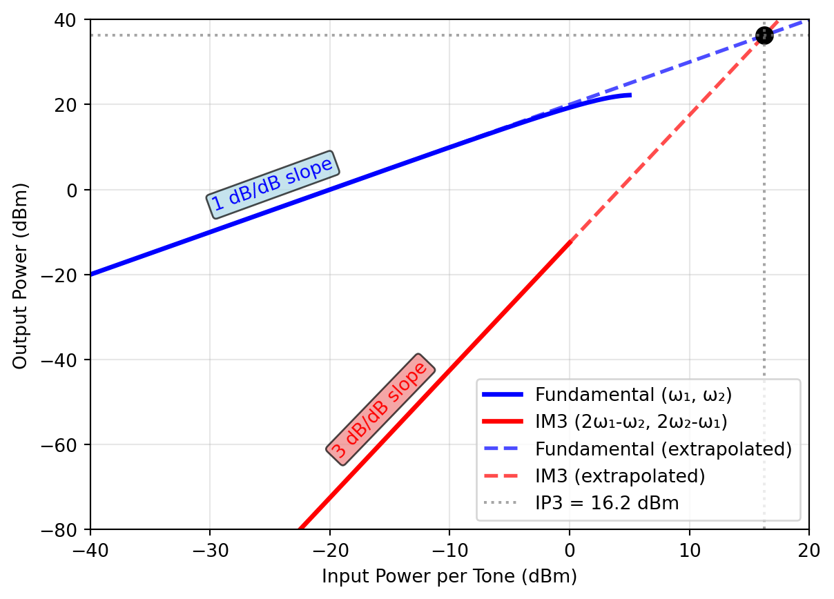
Note that, as shown in Figure 9, the IM3 products rise with a slope of 3 dB/dB, i.e., if the input power is increased by 1 dB, the IM3 products increase by 3 dB. The fundamental tones rise with a slope of 1 dB/dB (as long as we are in the linear region). The IP3 point is defined as the intersection of the extrapolated linear lines of fundamental and IM3 products. As both lines have different slopes, this intersection point is usually far outside the actual operating range of the circuit block under test!
When calculating the IIP3 (input-referred IP3), we can use the following formula, assuming equal input power per tone. It is important to always check the slope of the IM3 products to ensure that we are indeed in the third-order region! If the input power per tone is \(P_\mathrm{in}\) (in dBm) and the input-referred power of one IM3 tone is \(P_\mathrm{IM3}\) (in dBm), then the input-referred IP3 is given by
\[ \text{IIP3} = P_\mathrm{in} + \frac{P_\mathrm{in} - P_\mathrm{IM3}}{2} \tag{12}\]
Further, for mildly nonlinear systems (i.e., \(\alpha_3\) is dominant), the IIP3 can be approximated from the 1-dB compression point as (Razavi 2011)
\[ \text{IIP3}|_\mathrm{dBm} \approx P_\mathrm{1dB}|_\mathrm{dBm} + 9.6\,\text{dB}. \tag{13}\]
If we have multiple blocks which are cascaded, and we know the gain and IIP3 of each block, we can calculate the overall IIP3 of the cascade with the following approximation. An exact calculation is very involved, as the nonlinearities of the first block (and the resulting tones) will be processed by the second block, creating even more tones; this process escalates very quickly. However, for practical purposes, the following approximation is often sufficient:
\[ \frac{1}{\text{IIP3}_\text{total}} \approx \frac{1}{\text{IIP3}_1} + \frac{G_1}{\text{IIP3}_2} + \frac{G_1 G_2}{\text{IIP3}_3} \tag{14}\]
Here \(G_1\) is the linear gain of the first block, and \(\text{IIP3}_1\), \(\text{IIP3}_2\) are the input-referred IP3 of the first and second block, respectively. Note that all powers have to be in linear units when using Equation 14. An even more simplified version of Equation 14 can be used with all quantities given in dBm and dB, respectively:
\[ \text{IIP3}_\text{total} \approx \min \{ \text{IIP3}_1, \text{IIP3}_2 - G_1, \text{IIP3}_3 - G_1 - G_2 \} \tag{15}\]
A typical RF system cascade with multiple blocks and their individual IIP3 contributions is shown in Figure 10.

Note 4: Simple IIP3 Cascade Calculation
Let’s calculate the overall IIP3 of two cascaded blocks. The first block is a low-noise amplifier with an IIP3 of -10 dBm and a gain of 20 dB. The second block is a mixer that has a gain of 10 dB and an IIP3 of 5 dBm. What is the value of the overall IIP3?
Using Equation 15 we can quickly estimate:
\[ \text{IIP3}_\text{total} \approx \min \{ -10\,\text{dBm}, 5\,\text{dBm} - 20\,\text{dB} = -15\,\text{dBm} \} = -15\,\text{dBm} \]
We see that the overall IIP3 is limited by the linearity of the second block, as the first block amplifies all signals (including blockers) by 20 dB before they reach the second block.
2.3 Noise
Just as nonlinearity is a limiting factor for large signals, noise is the limiting factor for small signals. Noise is present in all electronic circuits and systems, and it is impossible to avoid it. However, we can try to minimize its impact on system performance.
Noise is usually characterized by its power spectral density (PSD) in units of Watts per Hertz (W/Hz). For example, thermal noise at room temperature has a one-sided PSD of approximately \(k T = 4 \times 10^{-21}\,\text{W/Hz}\), or \(-174\,\text{dBm/Hz}\) (using Boltzmann’s constant \(k = 1.38 \times 10^{-23}\,\text{J/K}\)). This means that if we have a bandwidth of 1 MHz, the total thermal noise power would be:
\[ P_\mathrm{thermal} = \text{PSD} \cdot B = -174\,\text{dBm/Hz} + 10 \log_{10} \left( \frac{1\,\text{MHz}}{1\,\text{Hz}} \right) = -114\,\text{dBm} \]
The PSD of noise can be flat vs. frequency (which is called “white noise”), or can decrease with frequency (e.g., “flicker noise” or “1/f noise”). Further, noise can be generated by resistors (thermal noise), semiconductors (shot noise, generation-recombination noise), etc. A detailed discussion of noise sources can be found in (Gray et al. 2009; Razavi 2017).
2.3.1 Types of Noise Generation
Resistors generate thermal noise (also called Johnson-Nyquist noise), which is white noise with a one-sided PSD of \(4 k T R\) (in V\(^2\)/Hz) when looking at the voltage across the resistor, or \(4 k T / R\) (in A\(^2\)/Hz) when looking at the current through the resistor. This noise is generated by the random thermal motion of charge carriers in the resistor.
ImportantThermal Noise
Note that the simple approximation given above is only valid for reasonably low frequencies and typical temperatures, and is known as the Rayleigh-Jeans approximation. The full expression of Planck’s blackbody radiation, accounting for quantum effects, is given by (Pozar 2011)
\[ \text{PSD} = \frac{4 R h f}{e^{{h f}/{k T}} - 1} \]
where \(h\) is the Planck constant (\(h = 6.626 \times 10^{-34}\,\text{J s}\)) and \(f\) is the frequency. The Rayleigh-Jeans approximation is valid for \(f \ll k T / h\), which is approximately 6 THz at room temperature (290 K).
We can integrate the above single-sided PSD over the full frequency range and show that the rms noise voltage of a resistor \(R\) is bounded to
\[ \overline{v_\mathrm{n}^2} = \int_0^\infty \frac{4 R h f}{e^{{h f}/{k T}} - 1} df = \frac{2 (\pi k T)^2}{3 h} \cdot R \]
which equates to approximately 13 mVrms noise voltage for a 1 k\(\Omega\) resistor at room temperature (which is impossible to measure in practice, as there will be some form of bandwidth limitation in any real measurement setup).
MOSFETs generate several types of noise, the most important ones being the thermal noise of the channel and flicker noise.
The thermal noise of the channel can be modeled as a current noise source between the drain and source terminals with a one-sided PSD of \(\overline{I_\mathrm{n}^2} = 4 k T \gamma g_{d0}\) (in A\(^2\)/Hz), where \(\gamma\) is a process-dependent parameter (usually between 2/3 and 2). The parameter \(g_{d0}\) is the drain-source conductance of the MOSFET at \(V_\mathrm{DS} = 0\) (i.e., in deep triode); in saturation it is commonly approximated by \(g_{d0} \approx g_\mathrm{m}\).
In saturation, it is often useful to express the thermal noise as a voltage noise source at the gate with a PSD of \(\overline{V_\mathrm{n}^2} = 4 k T \gamma / g_\mathrm{m}\) (in V\(^2\)/Hz). We can see that we can lower this noise of the MOSFET by increasing the transconductance \(g_\mathrm{m}\), which can be achieved by increasing the bias current.
In addition, at high frequencies, the MOSFET also has induced gate-current noise, which is correlated with the channel thermal noise. A detailed discussion of this noise source can be found in (Razavi 2017).
Flicker noise is usually modeled as a voltage noise source at the gate with a PSD of \(K_f / (C'_\mathrm{ox}W L f)\) (in V\(^2\)/Hz), where \(K_f\) is a process-dependent parameter, \(C'_\mathrm{ox}\) is the oxide capacitance per unit area, \(L\) and \(W\) are the length and width of the MOSFET, and \(f\) is the frequency. Note that we can lower the flicker noise by increasing the area of the MOSFET (\(W \cdot L\)), however, this increases the parasitic capacitances associated with the MOSFET, and this is often prohibitive for RF operation!
In bipolar junction transistors (BJTs), the most important noise source is the shot noise due to the diffusion current in the base-emitter junction. It can be modeled as a current noise source between the collector and emitter terminals with a one-sided PSD of \(2 q I_\mathrm{C}\) (in A\(^2\)/Hz), where \(q\) is the elementary charge (\(q = 1.6 \times 10^{-19}\,\text{C}\)) and \(I_\mathrm{C}\) is the dc collector current.
ImportantEquivalence of Shot and Thermal Noise
Note that it has been shown in (Sarpeshkar et al. 1993) that thermal noise and shot noise are actually equivalent, as both are generated by the random, thermally agitated motion of charge carriers!
Ideal capacitors and inductors do not generate noise; however, real-world capacitors and inductors have parasitic resistances which generate thermal noise.
In RF systems, additional noise sources can be present. One noteworthy example is the cosmic microwave background radiation, which can be modeled as a noise temperature of approximately 3 K. While this is negligible compared to thermal noise at room temperature (approximately 290 K), it can be significant in very low-noise systems, such as radio telescopes pointing to the sky. Another important noise source in RF systems is the atmospheric noise, which is generated by natural phenomena like lightning or in the ionosphere.
NoteA Note on Circuit Noise Calculations
When doing circuit noise calculations, it is instructive to keep the following points in mind:
- For circuit calculations involving noise sources, it is convenient to replace the power spectral density by equivalent sinusoidal generators in small bandwidths (typically 1 Hz).
- The noise power spectral density in a small bandwidth \(\Delta f\) is given by \(\overline{V_\mathrm{n}^2} = \overline{v_\mathrm{n}^2} / \Delta f\) and \(\overline{I_\mathrm{n}^2} = \overline{i_\mathrm{n}^2} / \Delta f\).
- The quantities \(\overline{V_\mathrm{n}^2}\) and \(\overline{I_\mathrm{n}^2}\) can be considered the mean-square value of sinusoidal generators. Using these values, network noise calculations reduce to familiar sinusoidal circuit-analysis calculations using \(V_\mathrm{n}\) and \(I_\mathrm{n}\).
- Multiple independent noise sources can be calculated individually at the output, and the total noise in bandwidth \(\Delta f\) is calculated as a mean-square value by adding the individual mean-square contributions from each sinusoid.
2.3.2 Noise in Impedance-Matched Systems
We now want to calculate the maximum noise power that can be extracted from a noisy source. We assume the following situation as shown in Figure 11. Note that the voltage source \(\overline{V_\mathrm{n,s}^2}\) models the thermal noise of the source resistor \(R_\mathrm{s}\) resulting in a Thevenin equivalent circuit.

We know that the noise of the source resistor is given by \(\overline{V_\mathrm{n,s}^2} = 4 k T R_\mathrm{s}\). We assume the load resistor \(R_\mathrm{load}\) as noiseless and matched to the source resistor, i.e., \(R_\mathrm{load} = R_\mathrm{s}\) for maximum power transfer. The noise power spectral density delivered to the load resistor is then given by
\[ P_\mathrm{n,load} = \frac{\overline{V_\mathrm{n,load}^2}}{R_\mathrm{load}} = \frac{\overline{V_\mathrm{n,s}^2}}{4 R_\mathrm{s}} = k T \tag{16}\]
The calculation of Equation 16 confirms the initial statement that the maximum noise power spectral density that can be extracted from a noisy source is \(k T\) (in W/Hz). This result is independent of the actual value of the source resistance \(R_\mathrm{s}\).
We can further generalize the thermal noise of any impedance as
\[ \overline{V_\mathrm{n}^2} = 4 k T \Re \{ Z \} \tag{17}\]
as for example in the complex impedance \(Z_\mathrm{ant}\) of an antenna. Since an antenna is a reciprocal device, if we measure its radiation impedance \(Z_\mathrm{rad}\) (for example with a vector network analyzer), we can calculate its thermal noise with Equation 17 to \(\overline{V_\mathrm{n}^2} = 4 k T \Re \{ Z_\mathrm{rad} \}\).
2.3.3 Noise Figure
In RF systems, we often want to quantify the noise performance of a circuit block or a complete system. The most widely used metric is the noise factor (F), which is defined as the ratio of the signal-to-noise ratio (SNR) at the input to the SNR at the output of a circuit block or system. If we express the noise factor in dB, we call it the noise figure (NF) (Pozar 2011). The noise factor is given by
\[ F = \frac{\text{SNR}_\mathrm{in}}{\text{SNR}_\mathrm{out}} = \frac{(P_\mathrm{s}/P_\mathrm{n})_\mathrm{in}}{(P_\mathrm{s}/P_\mathrm{n})_\mathrm{out}} \tag{18}\]
where \(P_\mathrm{s}\) is the signal power and \(P_\mathrm{n}\) is the noise power. The noise factor is always larger than or equal to 1 (or 0 dB), as no circuit can improve the SNR!
ImportantSNR Improvement
Note that the SNR can be improved by filtering, as filtering reduces the noise power. If the noise bandwidth is larger than the signal bandwidth, then the SNR can be improved without affecting the signal. However, this is not considered in the noise factor, as the noise factor assumes that both signal and noise pass through the same bandwidth.
Let us look at a simple model of a noisy circuit block as shown in Figure 12. The input signal \(S_\mathrm{in}\) is accompanied by noise \(N_\mathrm{in}\). By definition, it is assumed that the input noise power results from a matched resistor at \(T_0 = 290\,\text{K}\), so that \(N_\mathrm{in} = k T_0\). The circuit block has a power gain \(G\) and adds its own noise \(N_\mathrm{dut}\) to the output signal. For simplicity, we assume that the input and output of the circuit block are impedance matched to avoid reflections.

The output signal and noise powers are then given by
\[ S_\mathrm{out} = G S_\mathrm{in} \]
\[ N_\mathrm{out} = G N_\mathrm{in} + N_\mathrm{dut} \] The resulting noise factor can then be calculated as
\[ F = \frac{{S_\mathrm{in}}/{N_\mathrm{in}}}{{S_\mathrm{out}}/{N_\mathrm{out}}} = \frac{1}{G} \frac{G N_\mathrm{in} + N_\mathrm{dut}}{N_\mathrm{in}} = 1 + \frac{N_\mathrm{dut}}{G N_\mathrm{in}}, \]
in other words, the noise factor is 1 plus the ratio of the noise added by the device under test (DUT) to the amplified input noise.
Note that a noiseless block (\(N_\mathrm{dut} = 0\)) has a noise factor of \(F=1\). A passive block with loss factor \(L\) (and impedance matched at input and output) has a noise factor of \(F=L\) (in linear units), as it attenuates the signal and \(N_\mathrm{out} = N_\mathrm{in} = k T\) if everything is in thermal equilibrium.

If we have a cascade of multiple blocks, as shown in Figure 13, we can calculate the overall noise factor with the Friis formula (Pozar 2011)
\[ F_\mathrm{total} = 1 + (F_1 - 1) + \frac{F_2 - 1}{G_1} + \frac{F_3 - 1}{G_1 G_2} \tag{19}\]
where \(F_i\) and \(G_i\) are the noise factor and power gain of the \(i\)-th block, respectively. Note that all gains have to be in linear units (not dB) when using Equation 19. We can interpret Equation 19 as follows:
- The overall noise factor \(F_\mathrm{total}\) is always larger than or equal to the noise factor of the first block (\(F_1\)).
- The noise factor of the first block is the most important one, as the noise factors of the following blocks are reduced by the gain of all preceding blocks. This is especially important in RF receivers, where the first block is usually a low-noise amplifier (LNA) with a very low noise figure (e.g., 1 dB or less) and a high gain (e.g., 10 dB or more). This ensures that the noise of the following blocks is negligible.
- The noise factor of the last block is reduced by the gain of all preceding blocks, so it is usually not very important.
Here we also see a trade-off between noise and linearity, as shown by Equation 14 and Equation 19. For low noise, we should try to maximize \(G_1\), however, this will affect linearity (IIP3) in a negative way. As in many other situations in RF design, we have to find a good compromise between conflicting requirements.
2.3.4 Sensitivity
In RF receivers, we often want to know the minimum input signal power that can be detected with a certain SNR. This minimum input signal power is called the sensitivity of the receiver. The sensitivity can be calculated as
\[ P_\mathrm{in, min} = P_\mathrm{n} \cdot \text{SNR}_\mathrm{min} \cdot F \tag{20}\]
where \(P_\mathrm{n}\) is the noise power at the input, \(\text{SNR}_\mathrm{min}\) is the minimum detectable SNR (i.e., the SNR required to demodulate the signal with given accuracy in terms of bit error rate or signal fidelity), and \(F\) is the noise factor of the receiver. The input noise power can be calculated as
\[ P_\mathrm{n} = k T B \]
where \(k\) is Boltzmann’s constant, \(T\) is the temperature in Kelvin, and \(B\) is the noise bandwidth of the receiver. Expressing Equation 20 in dB/dBm we get the following formula:
\[ P_\mathrm{in, min}|_\mathrm{dBm} = -174\,\text{dBm/Hz} + \text{NF} + 10 \log_{10}(B/\text{Hz}) + \text{SNR}_\mathrm{min}|_\mathrm{dB} \tag{21}\]
where -174 dBm/Hz is the thermal noise PSD at room temperature (290 K). We can see that the sensitivity reaches lower dBm values with lower noise figure, smaller bandwidth, and lower minimum detectable SNR.
Note 5: Sensitivity Calculation for Wi-Fi
Let’s calculate the sensitivity of a Wi-Fi receiver operating at 5 GHz with a noise bandwidth of \(B = 80\,\text{MHz}\), a noise figure of \(\text{NF} = 7\,\text{dB}\), and a minimum detectable SNR of 25 dB. This high SNR means that a high-order modulation scheme (like 64-QAM) is used for high data rates.
Using Equation 21 we get: \[ P_\mathrm{in, min} = -174\,\text{dBm/Hz} + 7\,\text{dB} + 10 \log_{10} (80 \times 10^6) + 25\,\text{dB} \approx -63\,\text{dBm} \]
This means that the minimum input signal power that can be detected by the Wi-Fi receiver is approximately -63 dBm.
2.4 Modulation
In order to transmit information via an EM wave, we need to modulate the wave with the information signal. Looking at a simple sinusoidal carrier wave
\[ s(t) = A \cos(\omega_0 t + \varphi) \]
we see that we can change one or more of the following parameters to encode information:
- Amplitude \(A(t)\) (amplitude modulation, AM; the digital form is called amplitude-shift keying, ASK)
- Frequency \(\omega_0(t)\) (frequency modulation, FM; the digital form is called frequency-shift keying, FSK)
- Phase \(\varphi(t)\) (phase modulation, PM; the digital form is called phase-shift keying, PSK)
- Amplitude \(A(t)\) and phase \(\varphi(t)\) (quadrature amplitude modulation, QAM)
The modulation formats FM and PM have the advantage that the carrier amplitude \(A\) is constant, which makes them more robust against nonlinear distortion.
QAM is widely used in modern communication systems, as it allows to transmit more bits per symbol by combining amplitude and phase modulation. The QAM type with four different symbols is called QPSK. Higher-order modulation formats like 16-QAM, for example, use 16 different symbols, which can encode four bits per symbol (as \(2^4 = 16\)). Even higher-order QAM formats like 64-QAM (6 bits per symbol), 256-QAM (8 bits per symbol), 1024-QAM (10 bits per symbol), or 4096-QAM (12 bits per symbol) are also used in modern systems like Wi-Fi or LTE/5G NR.
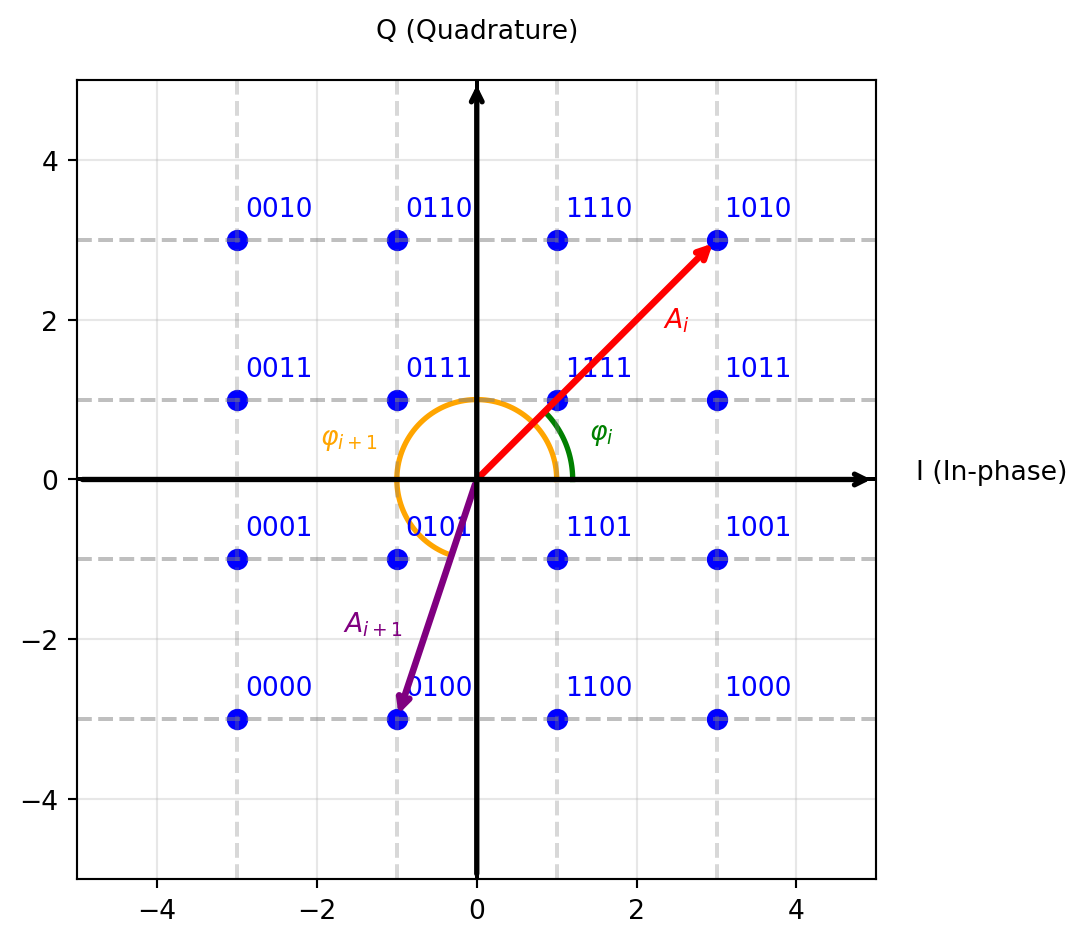
Shown in Figure 14 is the constellation diagram of a 16-QAM modulation format. The constellation points are arranged in a square grid, with each point representing a unique combination of amplitude and phase. The distance between the constellation points determines the robustness against noise and interference; larger distances result in better performance, but also require more power. The mapping of bits to constellation points is called “bit mapping” or “symbol mapping”. The example in Figure 14 uses a Gray code mapping, which minimizes the number of bit errors in case of a symbol error (assuming that a symbol will be wrongly decoded as one of its neighbors).
The constellation diagram can be imagined as a complex plane, where the x-axis represents the in-phase component (I) and the y-axis represents the quadrature component (Q) of the modulated signal. During transmission of a specific symbol, the RF carrier is modulated to the corresponding amplitude \(A_i\) and phase \(\varphi_i\), resulting in a specific point in the constellation diagram. In Figure 14, the amplitude and phase information for two consecutive symbols, \(A_i\)/\(\varphi_i\) and \(A_{i+1}\)/\(\varphi_{i+1}\), is shown. If we have a bitrate with a bit duration of \(T_\mathrm{b}\), the symbol duration for 16-QAM (4 bits per symbol) is \(T_\mathrm{s} = 4 T_\mathrm{b}\). During the first \(T_\mathrm{s}\), the carrier is modulated to \(A_i\)/\(\varphi_i\) (encoding 4 bits), and during the next \(T_\mathrm{s}\), it is modulated to \(A_{i+1}\)/\(\varphi_{i+1}\) (encoding the next 4 bits).
Table 3 shows the SNR requirements for different modulation formats to achieve a bit error rate (BER) of \(10^{-5}\) in an additive white Gaussian noise (AWGN) channel (Sklar and Harris 2020). As we can see, higher-order modulation formats require higher SNR to achieve the same BER. Note that for the SNR values of this table no error correction coding (ECC) is assumed; with error correction coding the required SNR can be significantly reduced!
| Modulation | Bits/Symbol | Required \(E_\mathrm{s}/N_0\) (dB) |
|---|---|---|
| BPSK | 1 | 9.6 |
| QPSK | 2 | 12.6 |
| 16-QAM | 4 | 18.2 |
| 64-QAM | 6 | 24.4 |
| 256-QAM | 8 | 30.6 |
| 1024-QAM | 10 | 36.9 |
| 4096-QAM | 12 | 43.2 |
2.5 Pulse Shaping and Spectral Efficiency
When we modulate symbols onto a carrier, the question is how we transition from one symbol \(A_i\)/\(\varphi_i\) to the next symbol \(A_{i+1}\)/\(\varphi_{i+1}\). If we change the amplitude and/or phase of the carrier instantaneously (like with a step function), we will have a very wide spectrum, which is not desirable.
Therefore, we often apply pulse shaping to the symbols, which means that we smooth the transitions between symbols. This is usually done by convolving the symbol sequence with a pulse shaping filter, which has a certain impulse response. The choice of the pulse shaping filter affects the bandwidth of the transmitted signal and its spectral efficiency.
A simple pulse shape is the rectangular pulse, which has a sinc-shaped spectrum. However, the function \(\text{sinc}(x) = \sin(\pi x)/(\pi x)\) has side lobes that extend to infinity and roll off only slowly, which can cause interference with adjacent channels.
For reference, the two-sided power spectral density \(S(f)\) of a random binary sequence with equal probability of \(-1\) and \(1\), using rectangular pulses with a duration of \(T_\mathrm{b}\), is given by (Sklar and Harris 2020)
\[ S(f) = T_\mathrm{b} \cdot \text{sinc}^2(fT_\mathrm{b}) = T_\mathrm{b} \cdot \left[ \frac{\sin(\pi f T_\mathrm{b})}{\pi f T_\mathrm{b}} \right]^2 \tag{22}\]
and visualized in Figure 15.
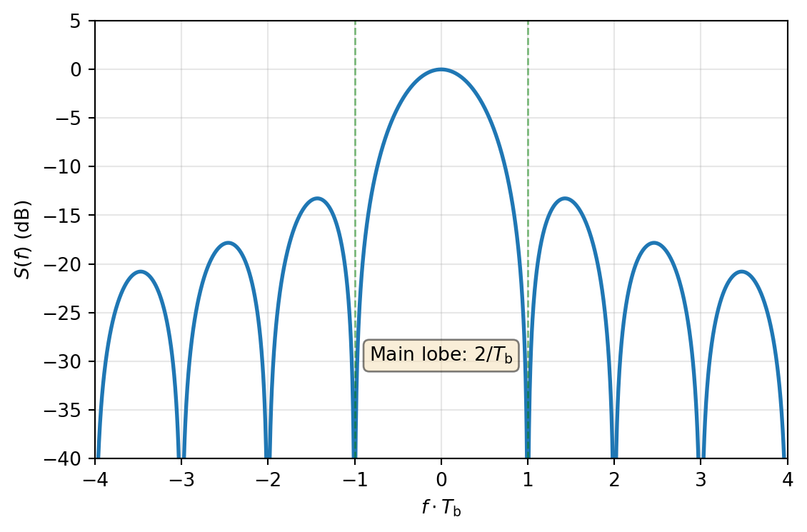
As can be seen in Figure 15, the main lobe of the sinc function has a bandwidth of \(2/T_\mathrm{b}\), but the side lobes are quite pronounced with a slow roll-off. This means that a significant amount of power is present outside the main lobe, which can cause interference with adjacent channels.
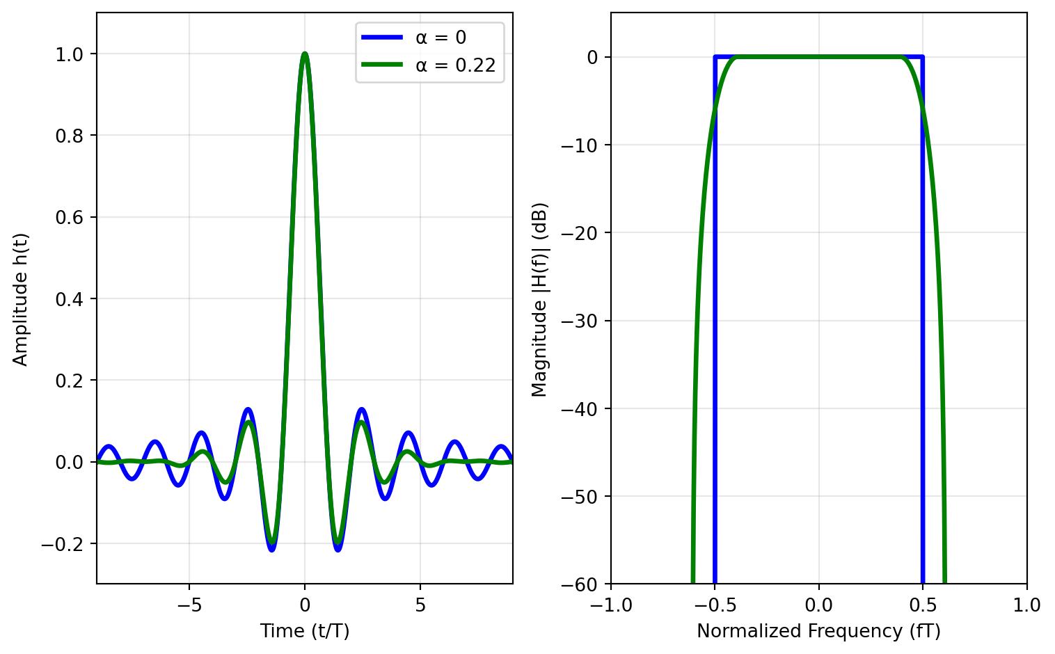
To avoid this, we can use pulse shapes that have better spectral properties, such as the raised cosine pulse or the root-raised cosine pulse. The raised-cosine pulse (see the raised-cosine filter, which satisfies the Nyquist ISI criterion) has a roll-off factor \(\alpha\) that determines the excess bandwidth beyond the Nyquist bandwidth. The root-raised cosine (RRC) pulse is used in practical systems (with half the pulse filter implemented at the TX, and half at the RX), as it can be implemented with a matched filter at the receiver.
The raised-cosine pulse \(p(t)\) (with a spectrum shaped like a raised cosine) is defined by:
\[ p(t) = \frac{\sin(\pi t / T_\mathrm{b})}{\pi t / T_\mathrm{b}} \cdot \frac{\cos(\alpha \pi t / T_\mathrm{b})}{1 - (2 \alpha t / T_\mathrm{b})^2} \]
Setting \(\alpha = 0\) results in a sinc pulse in the time domain (with a perfect bandwidth containment in the frequency domain), while \(\alpha = 1\) results in a pulse with double the Nyquist bandwidth. The pulse shape for \(\alpha = 0\) and \(\alpha = 0.22\) (used in 3G) is shown in Figure 16.
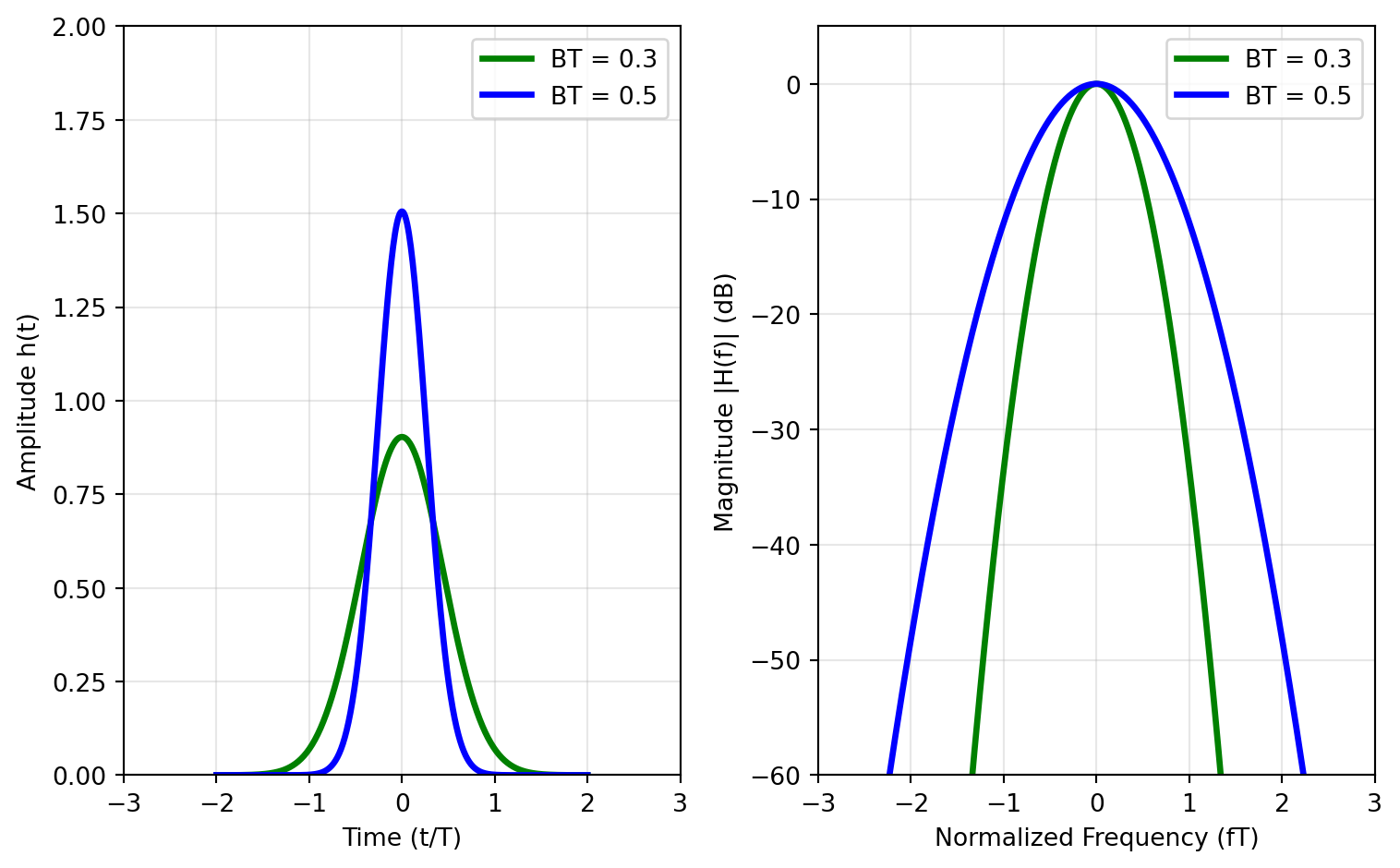
Another often-used pulse shape is the Gaussian pulse, which is used in Gaussian minimum-shift keying (GMSK, used in 2G) modulation, or in Gaussian frequency-shift keying (GFSK, used in Bluetooth). The Gaussian pulse has a smooth shape and a narrow spectrum. The Gaussian pulse is defined by:
\[ p(t) = \frac{\sqrt{\pi}}{\alpha} e^{-(\pi t / \alpha)^2} \quad \text{with} \quad \alpha = \frac{\sqrt{\ln 2}}{\sqrt{2}} \cdot \frac{T_\mathrm{b}}{B T_\mathrm{b}} \]
where \(B T_\mathrm{b}\) controls the width of the pulse. The spectrum of the Gaussian pulse is also Gaussian-shaped, which helps to minimize inter-symbol interference (ISI).
The Gaussian pulse for \(B T_\mathrm{b} = 0.5\) (as used in Bluetooth) is shown in Figure 17.
For all the shown pulse shapes (rectangular, raised-cosine, and Gaussian), the trade-off between time- and frequency-domain containment is clearly visible. This is also captured in “Küpfmüller’s uncertainty principle” (Küpfmüller 1949), which states that the product of the time duration and the bandwidth of a pulse is lower-bounded by a constant. In other words, if we want to have a pulse that is very short in time, it will have a wide bandwidth, and vice versa.
2.6 Orthogonal Frequency-Division Multiplexing (OFDM)
As we have seen in the previous section, if we make the symbol rate high, we need to use short pulses with a wide bandwidth. The problem with a wide bandwidth in wireless communication is multi-path propagation (Molisch 2022), which causes frequency-selective fading. This means that some frequency parts of the channel are attenuated more than others, which can cause errors in the received signal. Equalizing such a frequency-selective channel can be very complex, especially if the channel changes rapidly (as in mobile communication).
We now face a dilemma: How can we achieve high data rates (which require high symbol rates and thus wide bandwidth) while avoiding frequency-selective fading? The key idea, implemented in orthogonal frequency-division multiplexing (OFDM) (Molisch 2022), is to split the wideband channel into multiple narrow sub-channels (subcarriers), each with a low symbol rate. This way, each subcarrier experiences essentially flat fading, which is much easier to equalize.
The key question is now how to implement this idea efficiently, as we now have to apply modulation to hundreds or thousands of individual subcarriers. The solution is to use the inverse fast Fourier transform (IFFT) at the transmitter to generate the time-domain OFDM signal from the frequency-domain symbols, and the fast Fourier transform (FFT) at the receiver to recover the frequency-domain symbols from the time-domain OFDM signal. This process is illustrated in Figure 18.
The OFDM transmitter takes a block of \(N\) symbols (e.g., 64-QAM symbols) and maps them onto \(N\) subcarriers, thereby increasing the symbol duration \(T_\mathrm{sym}\) for each subcarrier to \(N \cdot T_\mathrm{b}\). The IFFT then generates the time-domain OFDM signal, which is transmitted over the wireless channel. Before transmission, the cyclic prefix (CP) is added to each OFDM symbol.
At the receiver, the CP is first removed, and then the FFT recovers the frequency-domain symbols, which can then be equalized (fairly simply by multiplying each subcarrier with a complex factor to correct amplitude and phase) and demodulated.
A key property of OFDM is that the subcarriers are orthogonal to each other, which means that they do not interfere with each other. This is achieved by choosing the subcarrier spacing \(\Delta f\) such that it is equal to the symbol rate \(1/T_\mathrm{sym}\), i.e., \(\Delta f = 1/T_\mathrm{sym}\). This way, the integral of the product of two different subcarriers over one symbol period is zero, which means that they are orthogonal.
To further improve the robustness against multi-path propagation, a CP is added to each OFDM symbol. The CP is a copy of the last part of the OFDM symbol, which is added to the beginning of the symbol. This way, if there are delayed copies of the OFDM symbol due to multi-path propagation, they will still fall within the CP and will not cause inter-symbol interference (ISI). The length of the CP should be longer than the maximum delay spread of the channel.
Note 6: OFDM in LTE
In LTE OFDM is used for the downlink (base station to user equipment) with the following parameters:
- Subcarrier spacing: 15 kHz
- CP length: 5.2 µs (first symbol) resp. 4.7 µs (following symbols), and 16.67 µs as extended CP for scenarios with large delay spreads
- Number of subcarriers: 1200 (for 20 MHz bandwidth)
- Modulation: QPSK, 16-QAM, 64-QAM, 256-QAM
From the subcarrier spacing we can calculate the symbol duration as \(T_\mathrm{sym} = 1 / \Delta f = 1 / 15\,\text{kHz} \approx 66.7\,\mu\text{s}\).
We can calculate the raw bitrate for a 20 MHz LTE channel using 256-QAM modulation as
\[ \text{Bitrate} = N_\mathrm{sc} \cdot N_\mathrm{bps} \cdot \frac{1}{T_\mathrm{sym} + T_\mathrm{CP}} = 1200 \cdot 8 \cdot \frac{1}{66.7\,\mu\text{s} + 4.7\,\mu\text{s}} \approx 134\,\text{Mbps} \]
With the overhead for control channels and error correction coding a user data rate of approximately 100 Mbps can be achieved in a 20 MHz LTE channel. This data rate can be scaled up by using multiple 20 MHz channels (MIMO, carrier aggregation).
2.7 Multiple Access Techniques
In wireless communication systems, multiple users need to share the same frequency spectrum. This is achieved by using multiple access techniques, which allow multiple users to transmit and receive data simultaneously without interfering with each other. The most common multiple access techniques are:
Time division multiple access (TDMA): Users are assigned specific time slots for transmission, allowing multiple users to share the same frequency channel by dividing continuous time into slots.
Frequency division multiple access (FDMA): Users are assigned specific frequency bands within the overall frequency spectrum, allowing multiple users to transmit simultaneously on different frequencies.
Code division multiple access (CDMA): Users are assigned unique spreading codes, allowing them to transmit simultaneously over the same frequency band. The receiver uses the same code to extract the desired signal. A variant of CDMA is frequency-hopping spread spectrum (FHSS), where the carrier frequency is changed rapidly according to a pseudo-random sequence known to both the transmitter and receiver. This is used in Bluetooth.
Orthogonal frequency division multiple access (OFDMA): A variant of OFDM, where multiple users are assigned different subcarriers for transmission, allowing for efficient use of the frequency spectrum. This is used in 4G LTE and 5G NR.
Spatial division multiple access (SDMA): Uses multiple antennas to create spatially separated channels, allowing multiple users to transmit simultaneously in the same frequency band.
All of the above techniques can be combined to create more efficient and flexible communication systems. For example, OFDMA can be used in conjunction with SDMA to allow multiple users to share the same frequency resources while also taking advantage of spatial diversity. Also, TDMA can be combined with FDMA to create a hybrid multiple access scheme (which has been used in 2G).
2.8 Modulation and Coding Schemes
In modern wireless communication systems several parameters can be adapted on the fly to the current channel conditions to optimize the data rate and reliability. These parameters include the modulation format (e.g., QPSK, 16-QAM, 64-QAM, etc.) and the error correction coding scheme (e.g., convolutional codes, turbo codes, LDPC codes, etc.). The combination of modulation format and coding scheme is called the modulation and coding scheme (MCS). The MCS determines the number of bits per symbol and the level of error correction, which in turn affects the data rate and reliability of the communication link, as well sets the minimum required SNR.
Since there are many different MCS options available, and the receiver needs to be informed by the transmitter which MCS is used (whenever there is a change of MCS), a standardized set of MCS options is defined in most wireless communication standards. For example, the MCS options for Wi-Fi can be seen in this table, while the MCS calculation for 5G NR can be found here.
NoteExemplary MCS in Wi-Fi
Some operating systems and wireless drivers show the MCS (and other parameters of the Wi-Fi link) during use. A typical output might be:
- MCS: 7
- RSSI: -53 dBm
- Interference: -92 dBm
- Bandwidth: 160 MHz
Looking up MCS 7 in the Wi-Fi MCS table linked above shows that this corresponds to 64-QAM with a coding rate of 5/6. With a bandwidth of 160 MHz, 2x MIMO and a guard interval (GI) of 0.8 µs, the maximum data rate is a whopping 1441 Mbps.
3 Transceivers
Nowadays, the various small-signal RF functions for receive and transmit are integrated into so-called transceivers (TRX). A TRX is a device that can both transmit and receive signals, and is usually called an “RFIC”. While high monolithic integration is certainly the norm for radio-frequency devices intended for standards like Bluetooth, Wi-Fi, cellular, etc., it is increasingly used also for mm-wave frequencies for applications like automotive radar and 5G cellular.
Typically, TRX include components like amplifiers, mixers, filters, oscillators, and phase-locked loops. When digital interfaces are used for the baseband I/Q data, also functions like analog-to-digital conversion (ADC) and digital-to-analog conversion (DAC) are integrated together with digital signal processing (DSP) blocks and potentially high-speed interfaces (because for wide bandwidths the I/Q sample rate can get quite high).
In these notes we will focus on the RF part of the TRX, which is responsible for the upconversion of baseband or intermediate frequency (IF) signals to the desired transmit frequency during transmission, and the downconversion of received signals from the carrier frequency to baseband or IF during reception. For filters, low-frequency amplifiers, ADCs, DACs, and DSP blocks we refer to related courses and literature, for example our analog circuit design course.
3.1 Direct-Conversion Transceiver
The following typical functions have to be performed by a TRX:
- Pulse-shaping filtering of the baseband signal (which can be implemented in analog or, in most cases, digital form).
- Modulating the baseband signal onto a carrier frequency (upconversion) in the TX or downconversion in the RX.
- Contain the RF signal in a small bandwidth (TX), or single out the wanted signal in the RX with adequate signal to noise ratio (SNR).
- Adapt gain (and linearity) to the signal strength in the RX, and to the output power in the TX.
- Generate the carrier frequency (local oscillator, LO) with low phase noise.
The dominant architecture for the TRX is the so-called direct-conversion or zero-IF architecture, where the up- and downconversion are performed in a single step (Razavi 2011). This is in contrast to super-heterodyne architectures, where the signal is first converted to an intermediate frequency (IF) before being converted to baseband. The direct-conversion architecture has the advantage of reduced complexity and cost, as it requires fewer components and less filtering. However, it also has some disadvantages, such as increased susceptibility to dc offsets and I/Q imbalance. A typical TRX block diagram is shown in Figure 19.

As can be seen in Figure 19, this generic architecture can be adapted in various ways. Generally, the amplifier gains are adjustable to adapt to different signal levels. If adaptive channel bandwidths are to be supported, the corner frequencies of the low-pass filters (LPF) can be adjusted, as well as (optionally) the sampling rate of the ADCs and DACs. The local oscillator (LO) frequency is generated by a phase-locked loop (PLL) synthesizer, which can be tuned to the desired carrier frequency. In case of frequency-division duplex (FDD) operation, two PLLs are used to generate the TX and RX LO frequencies, which are separated by the duplex distance \(f_\mathrm{dpx}\). In time-division duplex (TDD) operation, a single PLL is sufficient, supplying the LO signal to both RX and TX.
The modem (short for modulator-demodulator) that is shown in Figure 19 is responsible for the digital baseband processing, including functions like channel coding/decoding, modulation/demodulation, equalization, error correction, encryption/decryption, and framing/timing. The modem is usually implemented as a digital System-on-Chip (SoC) consisting of (multiple) CPUs, DSPs, and fixed-function blocks for time-critical processing. For an in-depth discussion we recommend (Sklar and Harris 2020) or (Molisch 2022).
3.2 Modulation and Demodulation
Modulation is the process of varying a carrier signal at frequency \(f_\mathrm{c}\) in order to transmit information. The complex baseband signal (after converting the real-valued in-phase and quadrature signals \(s_\mathrm{I}\) and \(s_\mathrm{Q}\), respectively, to analog and applying pulse-shaping filtering) is represented as (\(\tilde{s}_\mathrm{BB} \in \mathbb{C}\); \(s_\mathrm{I}, s_\mathrm{Q} \in \mathbb{R}\)) (Martin 2004):
\[ \tilde{s}_\mathrm{BB}(t) = s_\mathrm{I}(t) + j \cdot s_\mathrm{Q}(t). \]
We want to shift this signal to the carrier frequency \(f_\mathrm{c}\) to create the modulated RF signal \(\tilde{s}_\mathrm{RF} \in \mathbb{C}\), which can be done by multiplying with a complex exponential (\(e^{j \omega_\mathrm{c} t}\), with \(\omega_\mathrm{c} = 2 \pi f_\mathrm{c}\)):
\[ \tilde{s}_\mathrm{RF}(t) = \tilde{s}_\mathrm{BB}(t) \cdot e^{j \omega_\mathrm{c} t} = [s_\mathrm{I}(t) + j \cdot s_\mathrm{Q}(t)] \cdot [\cos(\omega_\mathrm{c} t) + j \cdot \sin(\omega_\mathrm{c} t)]. \]
The real-valued RF signal \(s_\mathrm{RF} \in \mathbb{R}\) is obtained from \(\tilde{s}_\mathrm{RF}\) by complex-conjugate symmetry:
\[ s_\mathrm{RF}(t) = \frac{1}{2} \left[ \tilde{s}_\mathrm{RF}(t) + \tilde{s}_\mathrm{RF}^*(t) \right] = s_\mathrm{I}(t) \cos(\omega_\mathrm{c} t) - s_\mathrm{Q}(t) \sin(\omega_\mathrm{c} t). \tag{23}\]
The process formulated in Equation 23 is done in hardware in the TX modulator, as shown in Figure 20.

The RF signal generation according to Equation 23 is called quadrature modulation. This is the modulation method used most often in modern (broadband) communication systems, as it allows one to transmit two independent signals (I and Q) in the same bandwidth. The I and Q signals are also called quadrature components, as they are 90° out of phase with each other.
Alternatively, a modulation method called polar modulation can be used, where the amplitude and phase of the carrier are varied according to (again using the complex-conjugate symmetry to obtain a real-valued signal):
\[ \begin{split} s_\mathrm{RF}(t) &= \frac{1}{2} \left[ A(t) \cdot e^{j \omega_\mathrm{c} t + j \varphi(t)} + A(t) \cdot e^{-j \omega_\mathrm{c} t -j \varphi(t)} \right]\\ &= A(t) \cdot \cos[ \omega_\mathrm{c} t + \varphi(t) ] \end{split} \]
This is done by converting the baseband I and Q signals (\(s_\mathrm{I}\) and \(s_\mathrm{Q}\)) to polar coordinates with
\[ A(t) = \sqrt{s_\mathrm{I}^2(t) + s_\mathrm{Q}^2(t)}, \quad \varphi(t) = \tan^{-1} \left[ \frac{s_\mathrm{Q}(t)}{s_\mathrm{I}(t)} \right]. \]
As the mathematical operations required for the Cartesian to polar transformation are quite nonlinear, the \(A(t)\) and \(\varphi(t)\) signals are wideband. While fairly complex to implement, polar modulation can have an efficiency advantage in the TX circuits, as the signal loss associated with quadrature combination can be avoided (Fulde et al. 2017).
For narrowband wireless standards the use of polar modulation can be quite efficient, as for example Bluetooth, where basically all transmitters are realized as polar modulators.
In the RX, the received RF signal is downconverted to baseband by the inverse process of Figure 20, shown in Figure 21.

For demodulation we have to shift the RF signal down to baseband, which mathematically is done by multiplying with the negative complex carrier frequency \(e^{-j \omega_\mathrm{c} t}\)
\[ \begin{split} \tilde{s}_\mathrm{BB}(t) &= s_\mathrm{RF}(t) \cdot e^{-j \omega_\mathrm{c} t}\\ &= s_\mathrm{RF}(t) \cdot [\cos(\omega_\mathrm{c} t) - j \cdot \sin(\omega_\mathrm{c} t)]\\ &= s_\mathrm{I}(t) + j \cdot s_\mathrm{Q}(t) \end{split} \tag{24}\]
with \(s_\mathrm{I}(t) = s_\mathrm{RF}(t) \cdot \cos(\omega_\mathrm{c}t)\) and \(s_\mathrm{Q}(t) = -s_\mathrm{RF}(t) \cdot \sin(\omega_\mathrm{c}t)\). Note that these products also generate components at \(2 \omega_\mathrm{c}\), which are removed by the subsequent low-pass filter; the recovered baseband signals additionally carry a factor of one-half that is compensated by the RX gain.
3.3 Filtering
Filtering is an essential function in both TX and RX. In the TX, filtering is used to limit the bandwidth of the transmitted signal to the allocated channel bandwidth, and to suppress out-of-band emissions. In the RX, filtering is used to select the wanted signal from a crowded spectrum, and to suppress unwanted signals (blockers) that can cause interference or desensitization of the RX.
A typical example of filtering in the RX is shown in Figure 22, where a bandpass filter is used to attenuate strong unwanted blockers while only slightly attenuating the wanted signal.
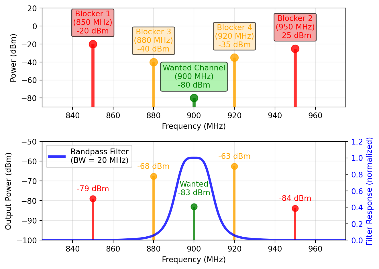
In any filter there exists a fundamental trade-off between selectivity (steepness of the filter skirts), bandwidth, and insertion loss. A very selective filter with steep skirts and large passband BW will have a high insertion loss. Conversely, a filter with low insertion loss will have a gentle roll-off and may not sufficiently suppress unwanted signals.
A useful metric to quantify the performance of a filter is the quality factor \(Q\), defined as
\[ Q = \frac{f_\mathrm{c}}{\Delta f} \]
where \(f_\mathrm{c}\) is the center frequency and \(\Delta f\) is the \(-3\) dB bandwidth of the filter. A high \(Q\) indicates a narrow-band filter.
The achievable \(Q\) depends on the used filter technology. For example, on-chip \(LC\) filters can achieve \(Q\) values of around 10–20, while off-chip SAW or BAW/FBAR filters can achieve \(Q\) values of several hundreds, and a crystal filter can achieve \(Q\) values of several thousands.
The choice of filter technology depends on the application requirements, such as frequency range, bandwidth, insertion loss, cost, and power handling. Generally speaking, the required filtering to single out the wanted signal in the RX spectrum and decrease the power of strong blockers to a tolerable level is one of the most critical design choices, and is usually distributed at different locations in the RX chain:
- RF filters (between antenna and LNA) provide a first level of filtering, and are usually implemented as off-chip SAW or BAW/FBAR filters. They provide high \(Q\) and good selectivity, but have a fixed center frequency and bandwidth. They are used to pass the wanted band of interest, and to attenuate strong out-of-band blockers.
- IF filters (in case of a super-heterodyne receiver) provide additional filtering, and can be implemented as on-chip LC filters or off-chip SAW/BAW filters. They provide moderate \(Q\) and selectivity, and can be tuned to some extent.
- BB filters (after downconversion) provide the final level of filtering before entering the ADCs, and are usually implemented as on-chip active \(RC\) filters. They provide channel selection, and can be easily adjusted to different bandwidths.
- Digital filters (in the DSP block) provide the final level of filtering and signal processing, and can be implemented as FIR or IIR filters. They provide high flexibility and can be easily adapted to different standards and requirements. Digital filters show no variations, so they can be designed to be very selective.
It is important to note (because this dictates a lot of choices in RF design) that high-\(Q\) filters are usually fixed-frequency and fixed-bandwidth. Only baseband and digital filters can be easily adjusted to different bandwidths!
NoteFilter Technologies Primer
Baseband filters (analog) are usually implemented as active \(RC\) filters on-chip (Schaumann et al. 2009; Zverev 1967). They are very flexible and can have adjustable bandwidth by changing \(R\) and/or \(C\). For medium/high frequencies \(g_\mathrm{m}C\) filters can be used, which are also tunable by changing the transconductance \(g_\mathrm{m}\) and/or \(C\). For even higher bandwidths, on-chip LC filters can be used, which have a limited \(Q\) of around 10–20.
Baseband filters (digital) are implemented as FIR or IIR filters. They can be made programmable and can be easily adapted to different requirements. Digital filters show no variations, so they can be designed to be very high performance. However, a trade-off between power consumption/area (number of bits and operations) and performance exists.
Surface acoustic wave (SAW) and bulk acoustic wave (BAW/FBAR) filters are specialized off-chip components that can achieve high \(Q\) into the thousands. They have a fixed center frequency and bandwidth. Usually 1–2 such filters are required per supported band of interest, which can drive up implementation cost and PCB area for RF front-ends that shall support many different frequency bands.
Crystal filters can achieve very high \(Q\) values of several tens of thousands, but are usually bulky and expensive and limited to an operating frequency of tens of MHz.
LC filters can be either implemented off-chip (using discrete components) or on-chip. Off-chip \(LC\) filters can achieve higher \(Q\) values than on-chip \(LC\) filters, but are usually larger and more expensive. On-chip \(LC\) filters are limited in \(Q\) (around 10–20), but are very compact and can be integrated into the RFIC. Off-chip \(LC\) filters can achieve \(Q\) values of around 50–100, depending on the frequency and component quality. \(LC\) filters can be made tunable by changing \(L\) (difficult) and/or \(C\) (easy).
Ceramic filters are another off-chip filter technology that can achieve moderate to high \(Q\) values (up to several hundreds). They are usually smaller and less expensive than SAW or BAW/FBAR filters, but also have lower performance.
Waveguide filters are used at very high frequencies (above 10 GHz) and can achieve very high \(Q\) values (up to several thousands). They are usually bulky and expensive, and are not commonly used in mobile applications, but rather in fixed installations like base stations or satellite communication.
Optical filters can have extremely high \(Q\) values but are difficult to apply in electronic RF systems due to the need for optical components and the challenge of integrating them with electronic circuits, as well as the required electrical-optical signal conversion.
Fundamentally, the choice of filter technology is a trade-off between performance, size, cost, power handling, and flexibility. In most cases, a combination of different filter technologies is used to achieve the desired performance.
3.4 Direct-Conversion Architecture
The transceiver architecture shown in Figure 19 is called the direct-conversion or zero-IF architecture, as the downconversion in the RX and upconversion in the TX are done in a single step. This architecture has several advantages:
- Per RX- and TX-chain a single LO is required (which can even be shared between RX and TX in TDD operation).
- There are a minimum number of RF blocks, which is good for cost and power consumption.
- This architecture is very flexible and can be easily adapted to different standards and requirements, even for wideband operation. It generally shows very good performance if the disadvantages can be overcome by good design.
- This architecture allows a high integration level, as basically all blocks can be implemented on-chip.
- Direct conversion is the de facto standard architecture for cellular, Wi-Fi, Bluetooth (with the exception of the TX), and GNSS.
However, the direct-conversion architecture also has some serious disadvantages:
- LO-RF coupling can cause self-mixing and desensitization of the RX, as well as LO leakage in the TX. This is an issue because the LO frequency is the same as the RF carrier frequency.
- Even-order distortion (characterized by a low IIP2) causes sensitivity degradation due to strong amplitude-modulated blockers (Gebhard et al. 2019).
- LO pulling can occur in the TX (as, again, LO and RF are at the same frequency).
- I/Q errors (amplitude and phase mismatch) of the \(I\) and \(Q\) paths can cause constellation distortion leading to increased error vector magnitude (EVM).
- Significant dc offsets can occur due to self-mixing of LO leakage or the even-order distortion products (IM2).
- Flicker noise (1/f noise) upconversion can cause increased TX noise close to the carrier, as well as increased RX noise figure.
Nowadays there exist good design techniques to mitigate these disadvantages. However, in some cases (for example very high linearity requirements, or very high frequencies) other architectures like low-IF or super-heterodyne may be preferable.
3.5 Duplexing
In the block diagram of Figure 19, we have not yet considered how to share a single antenna between RX and TX. Essentially, there are two main methods to achieve this: frequency-division duplex (FDD) and time-division duplex (TDD).
A special case beyond FDD and TDD is full-duplex (FD), where RX and TX operate simultaneously in the same frequency band. Full-duplex is technically challenging, as it requires very high isolation between RX and TX, which is difficult to achieve in practice. For some special applications, like radar, full-duplex operation is possible, but for most communication systems FDD or TDD is used.
3.5.1 Frequency-Division Duplex (FDD)
In FDD, the RX and TX operate at different frequencies, separated by a duplex distance \(f_\mathrm{dpx} = | f_\mathrm{RX} - f_\mathrm{TX} |\). This allows simultaneous transmission and reception, which is beneficial for applications like voice communication where low latency is required. However, FDD requires two separate frequency bands, which can be a limitation in terms of spectrum availability. Additionally, FDD requires two PLLs to generate the RX and TX LO frequencies, which increases complexity and power consumption.
The RF RX and TX paths are connected to the antenna via a duplexer filter, which is a three-port device that allows signals to pass between the antenna and the RX or TX path, while isolating the RX and TX paths from each other. A typical FDD TRX block diagram is shown in Figure 23.

Advantages of FDD:
- RX and TX can operate simultaneously, which is beneficial for low-latency applications.
- There is no need for fast switching between RX and TX, which simplifies the timing control.
- FDD allows relaxed synchronization requirements between RX and TX and different users.
Disadvantages of FDD:
- Duplexer filters are costly components with significant insertion loss depending on filtering requirements.
- It requires two separate frequency bands, which can be a limitation in terms of spectrum availability and MIMO channel estimation.
- The strong TX leakage via the duplexer filter into the RX path causes severe desensitization of the RX, which requires high linearity and good filtering (50 dB to 60 dB).
- The RX and TX chains (including their PLLs) are operating simultaneously, which increases power consumption and can cause interference between the RX and TX paths (e.g., LO pulling).
3.5.2 Time-Division Duplex (TDD)
In TDD, the RX and TX share the same frequency band but operate at different times. This allows for more efficient use of the available spectrum, as the same channel frequency can be used for both transmission and reception. TDD is particularly well-suited for applications with asymmetric traffic patterns, where the data rate in one direction is significantly higher than in the other. However, TDD requires precise timing control to avoid interference between RX and TX periods, which can increase complexity.
In TDD, a single PLL can be used to generate the LO frequency for both RX and TX, which reduces complexity and power consumption. The RX and TX RF paths are connected to the antenna via a switch, which alternates between connecting the antenna to the RX path and the TX path. A typical TDD TRX block diagram is shown in Figure 24.

Advantages of TDD:
- More efficient use of the available spectrum, as the same frequency can be used for both RX and TX.
- A single PLL can be used for both RX and TX, which reduces complexity and power consumption.
- No duplexer is required (just a single band filter), which reduces cost and insertion loss.
- No RX blocking by own TX, which relaxes linearity and filtering requirements.
- MIMO is easier to implement, as all antennas can operate in the same frequency band.
Disadvantages of TDD:
- RX and TX cannot operate simultaneously, which can be a limitation for low-latency applications.
- TDD requires precise timing control to avoid interference between RX and TX periods, which can increase complexity.
- Synchronization between RX and TX and different users is required, which can be challenging in some scenarios.
3.5.3 Comparison of FDD and TDD
Below is a summary of important wireless standards and their duplexing method as shown in Table 4.
| Wireless Standard | Duplexing Method | Comments |
|---|---|---|
| GSM (2G) | FDD & TDMA | TX and RX operate at different frequencies (FDD) and different times (TDMA) |
| UMTS (3G) | FDD | Traditional cellular standard using paired spectrum |
| LTE (4G) | FDD/TDD | FDD is used mostly <2.7 GHz, TDD is used >2.3 GHz |
| 5G NR | FDD/TDD | FDD is used mostly <2.7 GHz, TDD is used >2.3 GHz |
| Wi-Fi (802.11) | TDD | Unlicensed spectrum operation |
| Bluetooth | TDD | Short-range personal area network |
| Zigbee | TDD | Low-power IoT applications |
As you can see in Table 4, there is a tendency to use FDD for lower frequencies and long communication distances, while TDD is preferred for higher frequencies and shorter distances.
3.5.4 Full Duplex (FD)
In case of FD, neither a duplexer nor a switch can be used in the RF front-end. One popular method (which also helps to increase the RX-TX isolation) is to use two antennas, as shown in Figure 25. The TX antenna is used to transmit the signal, while the RX antenna is used to receive the signal. The two antennas are placed in such a way that they are isolated from each other, which helps to reduce the interference between the RX and TX paths. Also polarization diversity can be used to further increase the isolation.

Another method to achieve FD operation is to use a circulator, which is a three-port device that allows signals to flow in one direction while isolating the other two ports. The circulator can be used to connect the RX and TX paths to the same antenna, while providing isolation between them. A typical FD TRX block diagram using a circulator is shown in Figure 26.

Regardless of whether two antennas or a circulator are used, the isolation between the TX and RX paths is always finite (typically only in the range of 15 dB to 20 dB for a circulator). As a consequence, a large fraction of the own (and strong) TX signal leaks directly into the sensitive RX port. Practical FD systems therefore require additional self-interference cancellation (also called leakage cancellation), performed in the RF/analog and/or digital domain, to suppress this residual TX leakage below the RX noise floor (Sadjina et al. 2020).
3.6 Specialty Architectures
In some cases, other architectures may be preferred over the direct-conversion architecture. During the evolution of wireless communication, many different architectures have been proposed and used. However, only a few of them are still relevant today. A few examples are shown next.
3.6.1 Super-Heterodyne Architecture
The super-heterodyne architecture is a widely used approach in radio. It works by mixing the incoming/outgoing RF signal with an LO to produce an intermediate frequency (IF) signal. This IF signal is then amplified and processed, allowing for better selectivity and sensitivity compared to direct-conversion architectures. Super-heterodyne receivers and transmitters are known for their excellent performance in terms of image rejection and dynamic range, making them suitable for a variety of applications, including traditional analog TV and radio broadcasting. A simplified block diagram of a super-heterodyne transceiver is shown in Figure 27.

When you compare Figure 19 with Figure 27, you can immediately appreciate the increased complexity of the super-heterodyne architecture. It requires two PLLs to generate the RX and TX LO frequencies, as well as additional mixers, amplifiers, and filters for the IF stage. This increases cost, power consumption, and size. However, the super-heterodyne architecture can provide better performance in terms of selectivity and sensitivity, especially in challenging RF environments with strong blockers, as it allows distributed filtering at RF, IF, and baseband frequencies.
One important aspect of super-heterodyne receivers is the choice of the intermediate frequency (IF). The IF should be high enough to allow for effective filtering and high image frequency rejection, but low enough to avoid excessive complexity and power consumption. Common IF frequencies range from a few MHz to several hundred MHz, depending on the application and frequency band.
The image frequency is a spurious frequency that can interfere with the desired signal, and is located at \(f_\mathrm{image} = f_\mathrm{RF} \pm 2 f_\mathrm{IF}\) (the sign depends on the selection of high-side or low-side mixing, which is an important design choice in superhets). To suppress the image frequency, an image-reject filter is either placed before (RX) or after (TX) the mixer. The design of this filter is critical, as it must provide sufficient attenuation of the image frequency while maintaining low insertion loss for the desired signal.
An alternative to image filtering is the use of active image rejection techniques, such as the Hartley or Weaver architectures (see image-reject mixer) (Razavi 2011). These techniques use additional mixers and phase shifters to cancel out the image frequency, allowing for improved performance without the need for a dedicated image-reject filter.
3.6.2 Low-IF Architecture
To avoid some of the issues of direct-conversion architectures (like dc offsets and flicker noise), a low-IF architecture can be used. In a low-IF architecture (which is a kind of a super-heterodyne architecture), the RX and TX signals are mixed to a low intermediate frequency (typically a few MHz to tens of MHz) in the analog domain instead of directly to baseband (the final mixing to baseband is done digitally). This allows for easier filtering of dc offsets and flicker noise, while still maintaining the benefits of a single LO and reduced complexity compared to super-heterodyne architectures. A low-IF architecture is shown in Figure 28.

The low-IF architecture is the de facto standard for Bluetooth receivers. Its advantage compared to direct-conversion vanishes for larger channel bandwidths, which is why it is not used for cellular or Wi-Fi (GSM receivers might be an exception).
One noteworthy disadvantage of low-IF architectures is the required \(\ge 2\times\) BW of the analog baseband filters and the ADCs/DACs compared to direct-conversion. This might cause increased power consumption in these blocks. Additionally, the low-IF architecture still requires careful design to mitigate issues like I/Q imbalance and LO leakage, although these issues are generally less severe than in direct-conversion architectures.
3.6.3 Direct-Modulated Oscillator and Direct-Detection Receiver (aka “Super Simple” Architecture)
For some applications with very low cost and low performance requirements, a super simple architecture can be used (for applications like a garage door opener). In this architecture, the RX and TX paths are stripped down to the bare minimum. A simple direct-detection receiver just uses an (optional) bandpass filter and a power detector, while a simple direct-modulated oscillator transmitter uses an oscillator and (optional) power amplifier. These simplified architectures are shown in Figure 29.

Despite the reduced architecture, digital amplitude-shift-keying (ASK) or on-off-keying (OOK) can be used. If the receiver is able to discriminate between frequencies (e.g., by using two RF filters with a power detector each), also frequency-shift-keying (FSK) can be used.
3.7 I/Q Imbalance
In direct-conversion and low-IF architectures, the I and Q paths are used to process the in-phase and quadrature components of the signal. Ideally, these paths should have identical gain and a 90° phase difference. However, in practice, there are always some mismatches between the I and Q paths, leading to I/Q imbalance. This imbalance can cause constellation distortion, leading to increased error vector magnitude (EVM) and degraded system performance.
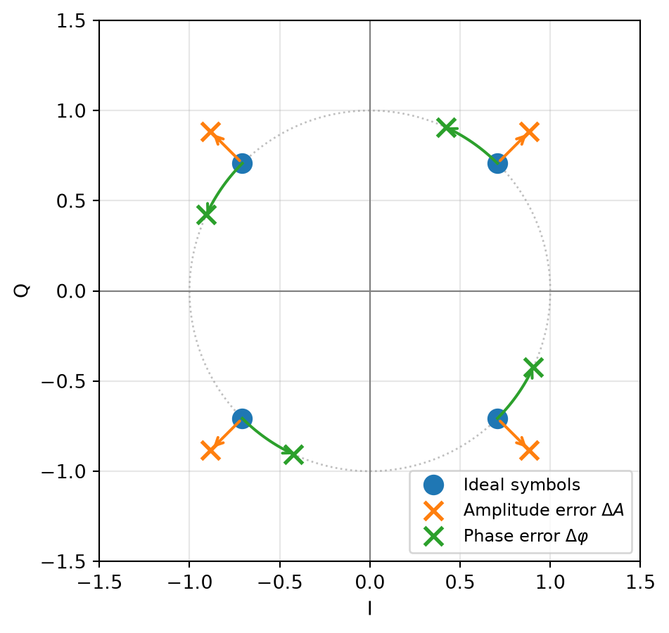
I/Q imbalance can be characterized by two parameters: amplitude mismatch (\(\Delta A\)) and phase mismatch (\(\Delta \varphi\)). Amplitude mismatch originates from the difference in gain between the I and Q paths, while phase mismatch refers to the deviation from the ideal 90° phase difference. The impact of I/Q imbalance on system performance depends on the modulation scheme used, with higher-order modulations being more sensitive to these impairments. Figure 30 illustrates both effects on a QPSK constellation: an amplitude mismatch displaces each symbol radially, while a phase mismatch rotates each symbol along the constellation circle.
There are two ways to quantify I/Q imbalance:
- Image rejection ratio (IRR): The IRR is a measure of how well the receiver can reject the image frequency caused by I/Q imbalance. It is defined as the ratio of the power of the desired signal to the power of the image (unwanted) signal, typically expressed in dB. A higher IRR indicates better performance, with values above 30 dB to 40 dB generally considered acceptable for most applications.
The IRR can be calculated from the relative amplitude mismatch \(\epsilon = \Delta A/A\) and the phase mismatch \(\Delta \varphi\) (in radians) as (Razavi 2011)
\[ \begin{split} \text{IRR} &= \frac{1 + (1 + \epsilon)^2 + 2 (1 + \epsilon) \cos(\Delta \varphi)}{1 + (1 + \epsilon)^2 - 2 (1 + \epsilon) \cos(\Delta \varphi)}\\ &\approx \frac{4}{\epsilon^2 + (\Delta \varphi)^2}, \end{split} \tag{25}\]
where the approximation on the right holds for small amplitude and phase errors. The IRR in dB is given by
\[ \text{IRR}|_\mathrm{dB} = 10 \cdot \log_{10}(\text{IRR}). \]
For example, an amplitude mismatch of 1% (\(\epsilon = 0.01\)) together with a phase mismatch of 1° (\(\Delta \varphi \approx 0.0175\)) yields an IRR of about 40 dB.
- Error vector magnitude (EVM): The EVM is a measure of the difference between the ideal transmitted signal and the received signal, expressed as a percentage of the signal’s magnitude. It quantifies the overall distortion in the received signal, including the effects of I/Q imbalance. Lower EVM values indicate better performance, with typical requirements ranging from 1% to 10% depending on the modulation scheme and application.
The EVM (in rms) is defined as
\[ \text{EVM} = \frac{\sqrt{\frac{1}{N} \sum_{i=1}^{N} |s_{\mathrm{ideal},i} - s_{\mathrm{meas},i}|^2}}{\sqrt{\frac{1}{N} \sum_{i=1}^{N} |s_{\mathrm{ideal},i}|^2}} \tag{26}\]
where \(s_{\mathrm{ideal},i}\) are the ideal transmitted symbols, \(s_{\mathrm{meas},i}\) are the measured received symbols, and \(N\) is the number of symbols. EVM is expressed either in percent or in dB using
\[ \text{EVM}|_\mathrm{dB} = 20 \cdot \log_{10}(\text{EVM}). \]
Note that the EVM (in dB) is always a negative number, with lower values indicating better performance. For example, an EVM of 1% (a very good number) corresponds to –40 dB, while an EVM of 10% corresponds to –20 dB. The SNR of the RF signal can be related to the EVM as
\[ \text{SNR}|_\mathrm{dB} \approx -20 \cdot \log_{10}(\text{EVM}) = -\text{EVM}|_\mathrm{dB}. \]
In order to make the I/Q mismatch sufficiently small, the following techniques can be used:
- Careful layout and matching of the components in the I and Q paths to minimize gain and phase mismatches. This usually involves good layout techniques. Further, the LO I/Q generation should be done with high accuracy.
- Calibration techniques can be used to measure and compensate for I/Q imbalance. This can be done either in the analog domain (e.g., using variable gain amplifiers and phase shifters) or in the digital domain (e.g., using digital signal processing algorithms). Digital compensation is usually preferred, as it is more flexible and can adapt to changing conditions. A CORDIC can be readily used for this purpose.
A final note on EVM: EVM is not only affected by I/Q imbalance, but also by other impairments like phase noise, nonlinearities, and noise in general. Therefore, EVM is a more comprehensive measure of the overall performance of a communication system, and often used to quantify the overall system performance in terms of SNR.
4 Low Noise Amplifiers
As shown in Section 2.3.4, the sensitivity of a receiver is determined (besides the channel bandwidth and the SNR requirement of the demodulator) mainly by the noise figure of the receiver. The noise figure is in turn determined by the noise figure of the first few components in the receive chain, as exemplified in Equation 19. Hence, as shown in Figure 23 and Figure 24, low noise amplifiers (LNAs) are usually the first active building block in a receiver after the antenna, switches, and initial RF filtering.
The main purpose of the LNA is to amplify the received signal with as little additional noise as possible, so that the subsequent stages in the receive chain can operate with a better signal-to-noise ratio (SNR) and do not increase the receiver NF substantially. The LNA is a critical component in the receiver design, and its performance has a significant impact on the overall sensitivity of the receiver.

The LNA as a building block is shown in Figure 31. It is usually designed for a specific frequency band, e.g., the 2.4 GHz ISM band or the 5 GHz WLAN band, and is typically designed for a specific impedance, e.g., 50 Ω, which is the standard impedance for RF systems. Impedance matching is usually mandated at the input; the output impedance matching is only required if the output of the LNA goes off-chip; if it is kept on-chip, impedance matching is often not needed. The LNA is also designed to be sufficiently linear, i.e., to not introduce significant distortion to the amplified signal; however, compared to the noise requirements, linearity is often less critical.
4.1 Impedance Matching
Why is impedance matching at the input of the LNA so important?
- The antenna is usually designed for a specific impedance, e.g., 50 Ω, and if the LNA input is not matched to this impedance, a significant portion of the received signal will be reflected back to the antenna, resulting in a loss of signal power.
- RF filters at the input of the LNA need to be terminated with the correct impedance to achieve the desired filter characteristics.
- Any transmission line in front of the LNA needs to be matched to avoid reflections and standing waves.
To quantify the “quality” of an impedance match, the reflection coefficient \(\Gamma\) is often used, which is defined as (Pozar 2011):
\[ \Gamma = \frac{Z_{\mathrm{in}} - Z_0}{Z_{\mathrm{in}} + Z_0} \tag{27}\]
where \(Z_0\) is the characteristic impedance of the system (usually 50 Ω) and \(Z_{\mathrm{in}}\) is the input impedance of the LNA. The reflection coefficient \(\Gamma\) is a complex number with a magnitude between 0 and 1 (as can be readily shown from Equation 27), where \(|\Gamma| = 0\) indicates a perfect match and \(|\Gamma| = 1\) indicates a complete mismatch. This reflection coefficient can be represented on the Smith chart shown in Figure 32. A useful interactive tool to draft a matching network and visualize it on a Smith chart is this website.
However, in practice, the more commonly used metric for impedance matching is the return loss (RL), which is defined as (Pozar 2011):
\[ \text{RL} = -20 \log_{10} |\Gamma| = 20 \log_{10} \left| \frac{Z_\mathrm{in} + Z_0}{Z_\mathrm{in} - Z_0} \right| \tag{28}\]
A higher return loss indicates a better impedance match. A return loss of 10 dB (see Figure 32) indicates that 10% of the signal power is reflected back, while a return loss of 20 dB indicates that only 1% of the signal power is reflected back. In practice, a return loss of at least 10 dB is desired, with higher (positive) values being better (Bird 2009).
NoteBode-Fano Criterion
The Bode-Fano criterion states that for a given load impedance and a given bandwidth, there is a fundamental limit to how well an impedance can be matched over that bandwidth; this criterion is important in the design of LNAs! The Bode-Fano criterion can be expressed mathematically as (Fano 1950; Pozar 2011, ch. 5.9)
\[ \int_{0}^{\infty} \ln \left( \frac{1}{|\Gamma(\omega)|} \right) d\omega \leq \frac{\pi}{R C} \tag{29}\]
where \(\Gamma(\omega)\) is the frequency-dependent reflection coefficient, \(R\) is the load resistance, and \(C\) is the load capacitance (for an \(R \parallel C\) load). This criterion implies that achieving a very good impedance match (i.e., a low reflection coefficient) over a wide bandwidth is fundamentally limited by the properties of the load. In practice, this means that there is a trade-off between the bandwidth of the match and the achievable return loss in an LNA design.
If we assume that we strive for match with \(|\Gamma_\mathrm{m}|\) over a fractional bandwidth \(\Delta \omega / \omega_0\), we can derive from the Bode-Fano criterion (and using that \(Q = \omega_0 R C\) for a parallel \(RC\) circuit) that
\[ \frac{\Delta \omega}{\omega_0} \leq \frac{\pi}{Q} \cdot \frac{1}{\ln(1/|\Gamma_\mathrm{m}|)} \]
For example, if we want to achieve a return loss of 20 dB (i.e., \(|\Gamma_\mathrm{m}| = 0.1\)) over a fractional bandwidth of 30%, we find that the quality factor of the load (i.e., the input stage of the LNA) needs to be \(Q \leq 4.5\).
4.2 Amplifier Stability
When designing amplifiers, it is generally important to ensure that the amplifier is stable, i.e., that it does not oscillate! Under well-defined conditions, this is already complicated enough, but in RF design, the situation is even more complex, as the stability is usually a function of source and load impedances, which, especially when going off-chip, are often not well defined.
Hence, we have a two-port network, where we need to ensure that the amplifier is stable for all possible source and load impedances, which represent a large number of potential simulation cases. Luckily, there are well-defined criteria to check the stability of a two-port network.
One test for unconditional stability is the Rollet stability factor \(K\), which is defined as (Pozar 2011)
\[ K = \frac{1 - |S_{11}|^2 - |S_{22}|^2 + |\Delta|^2}{2 |S_{12} S_{21}|} \tag{30}\]
with
\[ \Delta = S_{11} S_{22} - S_{12} S_{21}. \tag{31}\]
For unconditional stability, the following conditions must be met:
\[ K > 1 \quad \text{and} \quad |\Delta| < 1. \]
If these conditions are not met, the amplifier is potentially unstable, i.e., it might oscillate for some source and load impedances. In this case, further analysis is required to determine the stability of the amplifier.
Unfortunately, the \(K\)-factor test only provides a binary answer (stable/unstable) and does not provide any information about how close the amplifier is to instability. For this purpose, the so-called \(\mu\) stability factor is used, which is defined as (Edwards and Sinsky 1992)
\[ \mu = \frac{1 - |S_{11}|^2}{|S_{22} - S_{11}^* \Delta| + |S_{12} S_{21}|}. \tag{32}\]
For unconditional stability, the following condition must be met:
\[ \mu > 1 \]
The \(\mu\)-factor provides a measure of how close the amplifier is to instability; the larger the \(\mu\)-factor, the more stable the amplifier is. A \(\mu\)-factor of 1.5 or higher is usually considered sufficient for practical applications.
What we can learn from Equation 30, Equation 31, and Equation 32 is that to achieve a stable amplifier, we need to minimize the reverse gain \(S_{12}\) (also called isolation) and the input and output reflection coefficients \(S_{11}\) and \(S_{22}\). In practice, this means that we need to design the amplifier with good reverse isolation and good input and output matching. Cascode stages are often used in RF amplifiers to achieve high gain and good isolation.
4.3 Resistively Matched Common-Source LNA
The key question is now how to design an LNA with low noise figure and an input impedance matched to 50 Ω? In order to appreciate this design challenge, we will first try a naive approach, using a common-source amplifier with resistive termination, as shown in Figure 33.

If we assume the gate capacitance of \(M_1\) is negligible, we can achieve good input impedance matching by choosing \(R_\mathrm{p} = R_\mathrm{s} = 50\,\Omega\). The voltage gain of this simple common-source LNA is given by \(A_\mathrm{v} = -g_\mathrm{m}R_\mathrm{D}\), neglecting capacitances and \(g_\mathrm{ds}\) of \(M_1\) (we assume that the load tank is tuned to the desired frequency with \(\omega_0 = 1 / \sqrt{L C}\)).
How can we calculate the noise figure of this simple LNA? We formulate
\[ F = \frac{\text{total noise at output}}{\text{noise at output due to source only}}. \tag{33}\]
We derive a small-signal equivalent circuit of Figure 33, which is shown in Figure 34, to calculate the total noise at the output of the LNA.

With the help of Figure 34, we can calculate the total output noise power spectral density as
\[ \overline{V_\mathrm{n,out,1}^2} = A_\mathrm{v}^2 \cdot 4 k T (R_\mathrm{s} \parallel R_\mathrm{p}) = (g_\mathrm{m}R_\mathrm{D})^2 \cdot 4 k T (R_\mathrm{s} \parallel R_\mathrm{p}) \]
and
\[ \overline{I_\mathrm{n,out}^2} = 4 k T \gamma g_\mathrm{m}+ \frac{4 k T}{R_\mathrm{D}} \] \[ \overline{V_\mathrm{n,out,2}^2} = R_\mathrm{D}^2 \cdot \overline{I_\mathrm{n,out}^2} = 4 k T \gamma g_\mathrm{m}R_\mathrm{D}^2 + 4 k T R_\mathrm{D} \]
so that in total
\[ \begin{split} \overline{V_\mathrm{n,out}^2} &= \overline{V_\mathrm{n,out,1}^2} + \overline{V_\mathrm{n,out,2}^2}\\ &= 4 k T \left[ (g_\mathrm{m}R_\mathrm{D})^2 (R_\mathrm{s} \parallel R_\mathrm{p}) + \gamma g_\mathrm{m}R_\mathrm{D}^2 + R_\mathrm{D} \right]. \end{split} \tag{34}\]
We now need to find the output noise coming from the source only. For this we can use the equivalent circuit in Figure 35, to formulate the output noise due to the source only.

We find that
\[ \overline{V_\mathrm{n,out,s}^2} = A_\mathrm{v}^2 \cdot 4 k T R_\mathrm{s} \cdot \left(\frac{R_\mathrm{p}}{R_\mathrm{s} + R_\mathrm{p}} \right)^2. \tag{35}\]
Finally, we can use Equation 34 and Equation 35 with Equation 33 to calculate the noise figure of the simple resistively matched common-source LNA as
\[ F = \frac{\overline{V_\mathrm{n,out}^2}}{\overline{V_\mathrm{n,out,s}^2}} = 1 + \frac{R_\mathrm{s}}{R_\mathrm{p}} + \frac{\gamma R_\mathrm{s}}{g_\mathrm{m}(R_\mathrm{s} \parallel R_\mathrm{p})^2} + \frac{R_\mathrm{s}}{g_\mathrm{m}^2 (R_\mathrm{s} \parallel R_\mathrm{p})^2 R_\mathrm{D}}. \tag{36}\]
NoteCommon-source LNA with Resistive Matching
As an exercise to calculate noise behavior of circuits, derive and thus re-confirm the result of Equation 36 by yourself.
How can we interpret Equation 36? We see that we can minimize the noise factor by maximizing \(g_\mathrm{m}\). We then have a noise factor of
\[ F \overset{g_\mathrm{m}\gg}{=} 1 + \frac{R_\mathrm{s}}{R_\mathrm{p}} = 2 \]
so we see that we are limited to a minimum noise figure of 3 dB, even if we spend the bias current to make \(g_\mathrm{m}\) very large. We can go below a noise figure of 3 dB only if we give up on return loss and choose \(R_\mathrm{p} > R_\mathrm{s}\), however, this means that the input is no longer matched to 50 Ω, so there are bounds on how far we can go. Hence, this simple resistively matched common-source LNA is not a good choice for a low-noise amplifier, with one exception: For very wideband amplifiers, where an NF larger than 3 dB is acceptable, this configuration might be a good choice (often the solution shown in Section 4.4 is still better).
We see that we are stuck at high noise figures if we realize the real part of the input impedance with a resistor. This leaves us with the question of how to realize the real part of the input impedance otherwise. We will answer this question in the next sections (spoiler: feedback)!
4.4 Common-Gate LNA
We remember from our analog circuit design lecture that the common-gate configuration has an input impedance of \(1/g_\mathrm{m}\) (conveniently neglecting parasitic capacitances). Hence, if we choose \(g_\mathrm{m}= 1/50\,\Omega = 20\,\text{mS}\), we can achieve input matching to 50 Ω without using a resistor at the input. This is the key idea of the common-gate LNA, which is shown in Figure 36.

By inspecting Figure 36 and following the practice from Section 4.3, we can directly write down the output noise voltage as (setting \(g_\mathrm{m}^{-1} = R_\mathrm{s}\))
\[ \begin{split} \overline{V_\mathrm{n,out}^2} &= k T \left[ (g_\mathrm{m}R_\mathrm{D})^2 R_\mathrm{s} + \gamma g_\mathrm{m}R_\mathrm{D}^2 + 4 R_\mathrm{D} \right]\\ &= k T \left( \frac{R_\mathrm{D}^2}{R_\mathrm{s}} + \gamma \frac{R_\mathrm{D}^2}{R_\mathrm{s}} + 4 R_\mathrm{D} \right). \end{split} \tag{37}\]
The output noise due to the source only is given by
\[ \overline{V_\mathrm{n,out,s}^2} = k T \frac{R_\mathrm{D}^2}{R_\mathrm{s}}. \tag{38}\]
Finally, we can use Equation 37 and Equation 38 with Equation 33 to calculate the noise figure of the common-gate LNA as
\[ F = 1 + \gamma + \frac{4 R_\mathrm{s}}{R_\mathrm{D}} \approx 1 + \gamma \quad \text{for} \quad R_\mathrm{D} \gg R_\mathrm{s}. \tag{39}\]
With a classical long-channel \(\gamma = 2/3\), we can achieve a minimum noise figure of 2.2 dB, which is already better than the resistively matched common-source LNA in Section 4.3. However, using short-channel MOSFETs, \(\gamma\) is often larger than 1, so that the minimum noise figure of the common-gate LNA is often larger than 3 dB (Razavi 2011).
4.5 Inductively-Degenerated Common-Source LNA
As we have seen in Section 4.4, circuit techniques (feedback) can be used to realize the real part of an input impedance without the associated thermal noise of a resistor. We now try something different, in the hope that it will result in an even lower noise figure. We construct an LNA based on a common-source MOSFET amplifier, but we add an impedance \(Z_\mathrm{deg}\) into the source line for series-series feedback (Gray et al. 2009). This arrangement is shown in Figure 37.

We now extract the small-signal equivalent circuit of the input stage of Figure 37, which is shown in Figure 38, to calculate the input impedance (we ignore \(g_\mathrm{ds}\) for this analysis to simplify the derivation).

We find that
\[ V_\mathrm{x} = V_\mathrm{gs}+ Z_\mathrm{deg} (I_\mathrm{x} + g_\mathrm{m}V_\mathrm{gs}) \]
with \(V_\mathrm{gs}= I_\mathrm{x} / s C_\mathrm{gs}\), so that we can write the input impedance as
\[ Z_\mathrm{in} = \frac{V_\mathrm{x}}{I_\mathrm{x}} = \frac{1}{s C_\mathrm{gs}} + Z_\mathrm{deg} + \frac{g_\mathrm{m}Z_\mathrm{deg}}{s C_\mathrm{gs}}. \tag{40}\]
The final term in Equation 40 is the interesting one: By choosing \(Z_\mathrm{deg}\) to be inductive (which we can do by using either an on-chip or an off-chip inductor), we can realize a real part of the input impedance. Choosing \(Z_\mathrm{deg} = s L\), we find that
\[ Z_\mathrm{in} = \frac{1}{s C_\mathrm{gs}} + s L + \frac{g_\mathrm{m}L}{C_\mathrm{gs}}. \]
By proper choice of \(L\) and \(C_\mathrm{gs}\), we can achieve input matching to 50 Ω at the desired frequency \(\omega_0\). We find that the real part of the input impedance is given by
\[ \Re \{ Z_\mathrm{in} \} = \frac{g_\mathrm{m}L}{C_\mathrm{gs}}. \tag{41}\]
Without proof (refer to (Razavi 2011; Darabi 2020) for a derivation), we state the noise factor of this input stage (with some simplification) as (\(\omega_\mathrm{T} \approx g_\mathrm{m}/ C_\mathrm{gs}\) is the transition frequency of the MOSFET)
\[ \begin{split} F &= 1 + \frac{\gamma R_\mathrm{s} \omega_0^2 C_\mathrm{gs}^2}{g_\mathrm{m}}\\ &\approx 1 + \gamma R_\mathrm{s} g_\mathrm{m}\left( \frac{\omega_0}{\omega_\mathrm{T}} \right)^2\\ &\approx 1 + \gamma \omega_0^2 C_\mathrm{gs} L. \end{split} \tag{42}\]
Finally, we have an LNA input stage configuration that allows us to achieve a noise figure below 3 dB, even with \(\gamma > 1\), by proper choice of a fast transistor with \(\omega_\mathrm{T} \gg \omega_0\) (and thus small \(C_\mathrm{gs}\)). The inductively-degenerated common-source LNA is a widely used LNA input stage configuration in modern RFICs.
Note that the noise performance of Equation 42 cannot be lowered towards \(F=1\) because \(g_\mathrm{m}\), \(L\), and \(C_\mathrm{gs}\) are tied together by the input matching condition Equation 41, and we have neglected the induced gate noise of the MOSFET and other effects (Razavi 2011).
A bit more detailed schematic is shown in Figure 39. The inductor \(L_\mathrm{match}\) is used to match the input impedance to 50 Ω at the desired frequency, \(L_\mathrm{deg}\) is used to realize the real part of the input impedance, \(R_\mathrm{bias}\) is used to bias the gate of \(M_1\), \(M_2\) is a cascode transistor which increases the output impedance and thus the gain of the stage (plus it improves the reverse isolation), and \(R_\mathrm{D}\), \(L_\mathrm{D}\), and \(C_\mathrm{D}\) form a load tank which provides high gain at the desired frequency. A dc block is used at the input so that the bias point of \(M_1\) is not corrupted by the input signal source. The bias voltage \(V_\mathrm{bias2}\) sets the operating point of the cascode transistor \(M_2\).

What is missing in Figure 39 is a form of frequency tuning of the load tank to the frequency of interest, and support for different gain modes. Apart from these details, this LNA circuit is a good starting point for a practical LNA design.
4.6 Feedback LNA
One drawback of the inductively-degenerated common-source LNA (besides its limited bandwidth) is the use of at least one inductor. If the inductor is placed on-chip, it has a comparatively large size, and if it is implemented in the package (via a bondwire) or on the PCB it adds complexity or cost to the bill-of-materials (BOM).
As an alternative, if the CMOS technology is sufficiently fast, a shunt feedback amplifier, as shown in Figure 40, might be a good choice (Gray et al. 2009).

The input impedance of the shunt feedback LNA is given by
\[ Z_\mathrm{in} = \frac{Z_\mathrm{F} + Z_\mathrm{L}}{1 + g_\mathrm{m}Z_\mathrm{L}}. \tag{43}\]
NoteDerivation of the Shunt-Feedback Input Impedance
We apply a test voltage \(V_x\) at the gate and find the resulting current \(I_x\) (ignoring \(g_\mathrm{ds}\) and the gate capacitance for simplicity). Because the only path into the gate is through \(Z_\mathrm{F}\), we have
\[ I_x = \frac{V_x - V_d}{Z_\mathrm{F}}. \]
Applying KCL at the drain node, where currents leave through \(Z_\mathrm{F}\), through \(Z_\mathrm{L}\) to \(V_\mathrm{DD}\) (ac ground), and via the transistor current source \(g_\mathrm{m}V_x\):
\[ \frac{V_d - V_x}{Z_\mathrm{F}} + \frac{V_d}{Z_\mathrm{L}} + g_\mathrm{m}V_x = 0 \]
Rearranging for \(V_d\) and substituting back
\[ \begin{split} I_x &= \frac{V_x - V_d}{Z_\mathrm{F}}\\ &= \frac{V_x}{Z_\mathrm{F}} \cdot \frac{Z_\mathrm{F} + Z_\mathrm{L} - Z_\mathrm{L}(1 - g_\mathrm{m}Z_\mathrm{F})}{Z_\mathrm{F} + Z_\mathrm{L}}\\ &= \frac{V_x\,(1 + g_\mathrm{m}Z_\mathrm{L})}{Z_\mathrm{F} + Z_\mathrm{L}}, \end{split} \]
which gives Equation 43 directly.
The noise factor of the shunt feedback LNA is given by
\[ F = 1 + \left| \frac{Z_\mathrm{F} + R_\mathrm{s}}{g_\mathrm{m}Z_\mathrm{F} + 1} \right|^2 \cdot \frac{\gamma g_\mathrm{m}+ \Re \{ Y_\mathrm{L} \} }{\Re \{ Z_\mathrm{in} \}}, \tag{44}\]
which holds exactly for reactive (noiseless) \(Z_\mathrm{F}\) and \(Z_\mathrm{L}\) (where \(\Re\{Y_F\}=0\)), and for a matched input (\(R_\mathrm{s} = \Re\{Z_\mathrm{in}\}\)) (Darabi 2020).
As you can see from Equation 44, by making \(g_\mathrm{m}\) large (and spending enough bias current), the noise figure can be made arbitrarily small! Depending on the choice of \(Z_\mathrm{F}\) and \(Z_\mathrm{L}\), the input impedance of this LNA can be changed in interesting ways.
By setting \(Z_\mathrm{L} \rightarrow \infty\) (e.g., by biasing with a current source and high-impedance loading), we find that
\[ Z_\mathrm{in} = \frac{1}{g_\mathrm{m}} \]
which is independent of \(Z_\mathrm{F}\) and is a well-known result for a common-source stage. The disadvantage of this configuration is the noise factor, which (given that \(Z_\mathrm{F}\) is sufficiently large) tends towards \(F = 1 + \gamma\), which is the same as for the common-gate LNA.
A bit more interesting is the case when \(g_\mathrm{m}Z_\mathrm{L} = A_0\) and \(Z_\mathrm{L} \gg Z_\mathrm{F}\), which results in
\[ Z_\mathrm{in} = \frac{Z_\mathrm{L}}{1 + A_0} \]
which is the well-known result that the input impedance of an amplifier with feedback is reduced by the factor \(1 + A_0\), where \(A_0\) is the open-loop gain of the amplifier. The noise factor can be made small by making \(g_\mathrm{m}\) large, as we have already noted above.
A very interesting case can be achieved by choosing \(Z_\mathrm{L} = (s C_\mathrm{L})^{-1}\) and \(Z_\mathrm{F} = (s C_\mathrm{F})^{-1}\), which results in
\[ Y_\mathrm{in} = \frac{1}{Z_\mathrm{in}} = \frac{g_\mathrm{m}C_\mathrm{F}}{C_\mathrm{L} + C_\mathrm{F}} + s \frac{C_\mathrm{L} C_\mathrm{F}}{C_\mathrm{L} + C_\mathrm{F}} \tag{45}\]
Looking at Equation 45, we see that the input admittance has a real part! By proper choice of components, we can achieve an input impedance matched to 50 Ω at the desired frequency. The noise factor can again be made small by making \(g_\mathrm{m}\) large.
There is also an option, by proper choice of \(Z_\mathrm{F}\) and \(Z_\mathrm{L}\), to achieve an inductive input impedance component, which can be used to resonate out parts of the input capacitance of the LNA, similar to the inductively-degenerated common-source LNA. However, in contrast to the inductively-degenerated common-source LNA, no inductor is required in this case. This configuration is called a reactance-canceling LNA (Razavi 2011).
5 Mixers
As we have seen in Section 3.2, we are using mixers to “upconvert” and “downconvert” signals, i.e., we shift the frequency of a signal to a higher or lower frequency with the help of an auxiliary signal, called the “local oscillator” (LO) signal. The block diagram of a mixer is shown in Figure 41.

What we usually want in a mixer is that the input signal at \(\omega_\mathrm{in}\) is shifted by \(\omega_\mathrm{LO}\), so that the output signal is located at
\[ \omega_\mathrm{out} = \omega_\mathrm{in} \pm \omega_\mathrm{LO}. \]
It should be noted that the output signal usually contains additional frequency components, which are not desired. These so-called “spurious” components are usually filtered out in a subsequent filtering stage.
Recalling the properties of linear time-invariant (LTI) systems, we know that in an LTI system no new frequency components (which are not already present in the input signal) are generated. In conclusion, in order to generate new frequency components, a mixer has to be either
- a non-linear system, or
- a time-variant system.
Next we will look at two options on how to implement a mixer.
5.1 Non-Linear Mixer
Generally speaking, we can use any nonlinear device to implement a mixer (often, this generation of new frequency components in a nonlinear system is highly undesired; in a mixer, we want this effect). As a simple example we look at the case of a square function, shown in Figure 42.

When we apply the sum of the signals \(s_\mathrm{in}(t) = \cos( \omega_\mathrm{in} t)\) and \(s_\mathrm{LO}(t) = \cos(\omega_\mathrm{LO} t)\) to the input of a squarer, we get the output signal
\[ \begin{split} s_\mathrm{out}(t) = [ s_\mathrm{in}(t) + s_\mathrm{LO}(t) ]^2 &= \cos(\omega_\mathrm{in} t + \omega_\mathrm{LO} t) + \cos(\omega_\mathrm{in} t - \omega_\mathrm{LO} t) \\ &+ 1 + \frac{1}{2} \cos(2 \omega_\mathrm{in} t) + \frac{1}{2} \cos(2 \omega_\mathrm{LO} t). \end{split} \tag{46}\]
We see that the output signal contains the desired frequency components at \(\omega_\mathrm{in} \pm \omega_\mathrm{LO}\), but also additional components at dc (0 Hz), \(2 \omega_\mathrm{in}\), and \(2 \omega_\mathrm{LO}\). These additional components are usually unwanted and have to be filtered out in a subsequent filtering stage. As a side-note, in some circuits a frequency doubler is desired, which can be implemented by simply filtering out the other frequency components. In a doubler no LO signal is required, as the input signal is simply squared.
A simple example circuit is a diode, which has a non-linear current-voltage characteristic. The block diagram of a simple diode mixer is shown in Figure 43.

This structure is conceptually simple; it just requires a (fast) diode, filters to couple the desired frequency components in and out, and an RF choke to provide a dc bias voltage for the diode. However, the performance of such a simple mixer is usually not very good, as the diode is a highly non-linear device, which generates many spurious frequency components. More advanced mixer circuits use more complex non-linear devices (for example, a ring of diodes) to improve the performance. The advantage of these mixers is that they can operate up to very high frequencies (in the mm-wave range and beyond). If you can make a nonlinear device, you can make a mixer (think also of nonlinear optics, for example).
5.2 Time-Variant Mixer
In contrast to the non-linear mixer, a time-variant mixer uses an ideally linear device, but changes its properties over time. A simple example is a switch, which is opened and closed at the LO frequency. The block diagram of such a mixer is shown in Figure 44. This system is ideally linear from input to output, but very nonlinear when considering the LO input.

When the switch is closed (\(s_\mathrm{LO} \ge 0\)), the input signal is passed to the output, i.e., \(s_\mathrm{out}(t) = s_\mathrm{in}(t)\); when the switch is open (\(s_\mathrm{LO} < 0\)), no signal is passed, i.e., \(s_\mathrm{out}(t) = 0\). The output signal can be expressed as
\[ \begin{split} s_\mathrm{out}(t) &= s_\mathrm{in}(t) \cdot \underbrace{\frac{1}{2} \left\{ 1 + \mathrm{sgn}[ s_\mathrm{LO}(t) ] \right\}}_\text{Fourier series} \\ &= s_\mathrm{in}(t) \cdot \left[ \frac{1}{2} + \frac{2}{\pi} \sin(\omega_\mathrm{LO} t) + \frac{2}{3 \pi} \sin(3 \omega_\mathrm{LO} t) + \frac{2}{5 \pi} \sin(5 \omega_\mathrm{LO} t) + \ldots\right] \end{split} \]
where \(\mathrm{sgn}(\cdot)\) is the signum function. The term in curly brackets is a square wave that switches between 0 and 1 at the LO frequency. This square wave can be expressed as a Fourier series, which contains the fundamental frequency at \(\omega_\mathrm{LO}\) and all odd harmonics \(3 \omega_\mathrm{LO}\), \(5 \omega_\mathrm{LO}\), and so on. In conclusion, if the input signal is expressed as \(\cos(\omega_\mathrm{in} t)\), we get the output signal
\[ s_\mathrm{out}(t) = \frac{1}{\pi} \cos(\omega_\mathrm{in} t \pm \omega_\mathrm{LO} t) + \ldots \tag{47}\]
Again, we see that the output signal contains the desired frequency components at \(\omega_\mathrm{in} \pm \omega_\mathrm{LO}\), but also additional components at \(3 \omega_\mathrm{LO}\), \(5 \omega_\mathrm{LO}\), and so on. These additional components are usually unwanted and have to be filtered out in a subsequent filtering stage. The advantage of a time-variant mixer is that it can be implemented readily in CMOS, as shown in Figure 45.

The implementation in Figure 45 uses a single NMOS transistor as a switch. The LO signal is ac-coupled to the gate of the transistor, so that the dc operating point is set by the bias voltage \(V_\mathrm{bias}\). When the LO signal is high enough, the transistor is switched on and the input signal \(v_\mathrm{in}(t)\) is passed to the output; when the LO signal is low, the transistor is switched off and no signal is passed. Note that with the MOSFET we can switch voltages as well as currents, so the mixer can work in both modes, voltage mode or current mode.
A big disadvantage of this simple implementation is that the input signal is “lost” for half of the cycle when the MOSFET switch is open. A fully differential implementation (having differential ports at input, output and LO input) can alleviate this problem, as the input signal is always connected to one of the two output ports. This configuration is called a “double-balanced mixer” and is widely used in practice. It is shown in Figure 46.

Note that with a double-balanced mixer, we have 6 dB more conversion gain compared to the single-balanced mixer (refer to Equation 47), as can be seen in Equation 48. Note that the factor of \(2/\pi\) represents the conversion loss of an ideal double-balanced mixer of 3.9 dB.
\[ s_\mathrm{out}(t) = \frac{2}{\pi} \cos(\omega_\mathrm{in} t \pm \omega_\mathrm{LO} t) + \ldots \tag{48}\]
Note that no dc current needs to flow through the mixer structures shown in Figure 45 and Figure 46, which is a huge advantage when thinking of flicker noise. Flicker noise in a MOSFET is proportional to the dc current flowing through the device, so if no dc current flows, no flicker noise is generated!
In order to look at the full picture, we embed the mixer of Figure 46 in a complete RX front-end, as shown in Figure 47. An LNA (essentially a \(g_\mathrm{m}\) cell) creates a current signal from the received voltage signal at the antenna. This current signal is then fed to the mixer in the current domain, and further sunk into a transimpedance amplifier (TIA), which also implements a lowpass pole. The simplified circuit is shown in Figure 47.

The capacitors connected directly to ground at the mixer outputs are good practice, as they shunt high-frequency switching noise to ground, and in this way help the performance of the TIA, which otherwise would have to sink these currents. Note that all blocker currents originating at the LNA output and passing through the mixer are shunted by the feedback capacitors to the output of the TIA, and need to be actively driven by the TIA’s output stage!
5.3 Gilbert Cell Mixer
As we have seen in Section 5.2, in CMOS we have quite a few options to implement a mixer as the MOSFET is a good current and voltage switch. This is in stark contrast to the BJT, as the bipolar transistor can only be used as an (excellent) current switch in the differential pair configuration. Hence, we need to implement a current-mode mixer in bipolar technology. The most widely used structure is the so-called “Gilbert cell”, shown in Figure 48.

The idea is that an input transconductor creates currents, which are switched in the double differential pair and converted back to voltage in the load impedances. There are many known variations of this circuit, like skipping the current source at the bottom to increase linearity and headroom, or swapping the input transconductor for another structure. It might also be useful to “bleed” some bias current from the LO switching stage to improve the noise performance.
5.4 N-Path Filter
Without much deliberation or diving into the background, it has to be stated that passive mixers (based on MOSFET switches) have a few very interesting properties. One of them is that they can be used to implement very high-quality bandpass filters, called “N-path filters” (Lepage et al. 1953). The basic idea is shown in Figure 49. We use four phases of an LO signal to switch the four capacitors to ground in a round-robin fashion. The duty cycle of each LO phase is 25% to have a non-overlapping clock.

The key observation to make is that a switch that is opened and closed at a certain frequency (the LO frequency) can be seen as a time-variant resistor. This time-variant resistor converts impedance seen at one end to the other end, and also changes the frequency of this apparent impedance. In other words, if we connect grounded capacitors at one end of the mixer switches and look into the other end, we see a bandpass filter centered at the LO frequency! In this way we can build bandpass filters (and also bandstop filters (Vazny et al. 2010)) at very high frequencies which are precisely centered (without component variations) around \(\omega_\mathrm{LO}\).
The impedance characteristics of such a tank circuit exhibit first-order bandpass behavior, as shown in Figure 50. The peak impedance reaches 5.3 times the switch resistance (\(R_\mathrm{sw}\)), and importantly, the bandwidth is inversely proportional to the capacitance value, i.e., \(\mathrm{BW} \propto 1/C\). This relationship allows for precise control of the filter bandwidth by adjusting the capacitor values.
5.5 LO Generation
As you have seen in Section 3.2, for complex-valued modulation schemes (like QPSK, QAM, OFDM, and so on) we need to generate quadrature LO signals (i.e., two LO signals with a 90° phase shift). There are many ways to generate such signals, and we will now study a few of them.
5.5.1 RC/CR Phase Shift Network
Probably the simplest way to generate quadrature LO signals is to use a simple RC/CR phase shift network, as shown in Figure 51. The RC network (a first-order lowpass) generates a phase shift between 0° and -90°, while the CR network (a first-order highpass) generates a phase shift between 0° and +90°. By operating the network at \(\omega_0 = 1/RC\), we can achieve a 90° phase shift between the two outputs.

The advantage of this network is its simplicity, as it only requires a few passive components, and it can generate I and Q phases from an incoming signal at the target frequency. The disadvantage is that the phase shift is frequency-dependent, so the quadrature signals are only perfectly in quadrature at one frequency. Furthermore, the amplitude of the two outputs is not equal, which might require additional gain stages to equalize the amplitudes. Additionally, this passive network has a 3 dB loss, so we need additional gain stages to compensate for this loss.
5.5.2 Polyphase Filter
We can create a more advanced phase shift network (following the idea of Section 5.5.1) by using a so-called “polyphase filter” (Kaukovuori et al. 2008). The idea is to use multiple RC sections to create a more ideal phase shift network. An example is shown in Figure 52.

As shown in the figure above, we can use multiple stages (with \(R_1 C_1 \ne R_2 C_2\)) in cascade to broaden the frequency range over which we have a good 90° phase shift between the four outputs. The more stages we use, the better the performance, but also the more components are required. Note that this network is still passive, so it has an inherent loss, which also increases with the number of stages. The idea behind this network is that the network is transparent for positive frequencies, and blocks negative frequencies (or vice versa). We enter the network with real signals (having positive and negative frequency components), and at the output we get complex signals (having only positive or negative frequency components). In this sense this network is a complex filter.
Note that polyphase filters are popular when we have to create complex signals from real signals. We can use the polyphase filter in the LO path, or also in the signal path (e.g., in a receiver). The benefit is that we can work with a signal where the input frequency is equal to the output frequency. This is in strong contrast to the approach we will discuss next.
5.5.3 Flip-Flop Based Phase Generation
The most widely used approach to generate quadrature LO signals is to use digital circuits, as shown in Figure 53. The idea is to use a flip-flop (or a latch) to divide the frequency of an incoming clock signal by two. If we drive the two flip-flops (which are connected as toggle flip-flops) by inverted clocks, then the resulting output signals are 90° phase-shifted, as shown in Figure 54.


It is important to note that the circuit shown in Figure 53 has to be implemented in a way so that there is no phase ambiguity, i.e., the I-phase is lagging the Q-phase by exactly 90°. This can be achieved by using a reset signal to set the flip-flops to a known state at startup, or by implementing flip-flops using a differential clock input.
If the input clock is not 2x the target frequency but higher (e.g., 4x), then we can use a frequency divider approach to generate more than four phases. This could be useful in an N-path filter, where we could need more than four phases (see Section 5.4).
Often, we need four-phase LO signals with 25% duty cycle (instead of the 50% duty cycle shown in Figure 54). This can be achieved by using additional logic gates to combine the outputs of the flip-flops, as shown in Figure 55. The resulting LO waveforms are shown in Figure 56.


The advantage of using flip-flops to generate multi-phase LO signals is that very precise phase shifts can be achieved, which can be produced over a very wide frequency range. They can be implemented in different logic styles, like CMOS, ECL, CML, and so on. The disadvantage is that we need a high-frequency clock signal above the target frequency, which might be difficult to generate. Still, I/Q generation with flip-flops is the de-facto standard approach in modern RFICs.
5.5.4 Delay-Based Phase Generation
The final approach we want to mention is to use a delay line (or multiple ones) to generate phase shifts. Using transmission lines, this approach is widely used at very high frequencies, where other approaches (like the ones shown in Section 5.5.2 or Section 5.5.3) are difficult to implement. One well-known approach is the 90° hybrid coupler, realized with \(\lambda/4\) transmission lines (Pozar 2011). When the frequencies are high enough (and the resulting wavelengths short enough), this approach can even be implemented on-chip. The disadvantage is that the phase shift is frequency-dependent, so the quadrature signals are only perfectly in quadrature at one frequency. Furthermore, this passive network has a 3 dB loss, so we need additional gain stages to compensate for this loss. A branch-line hybrid coupler is shown in Figure 57.
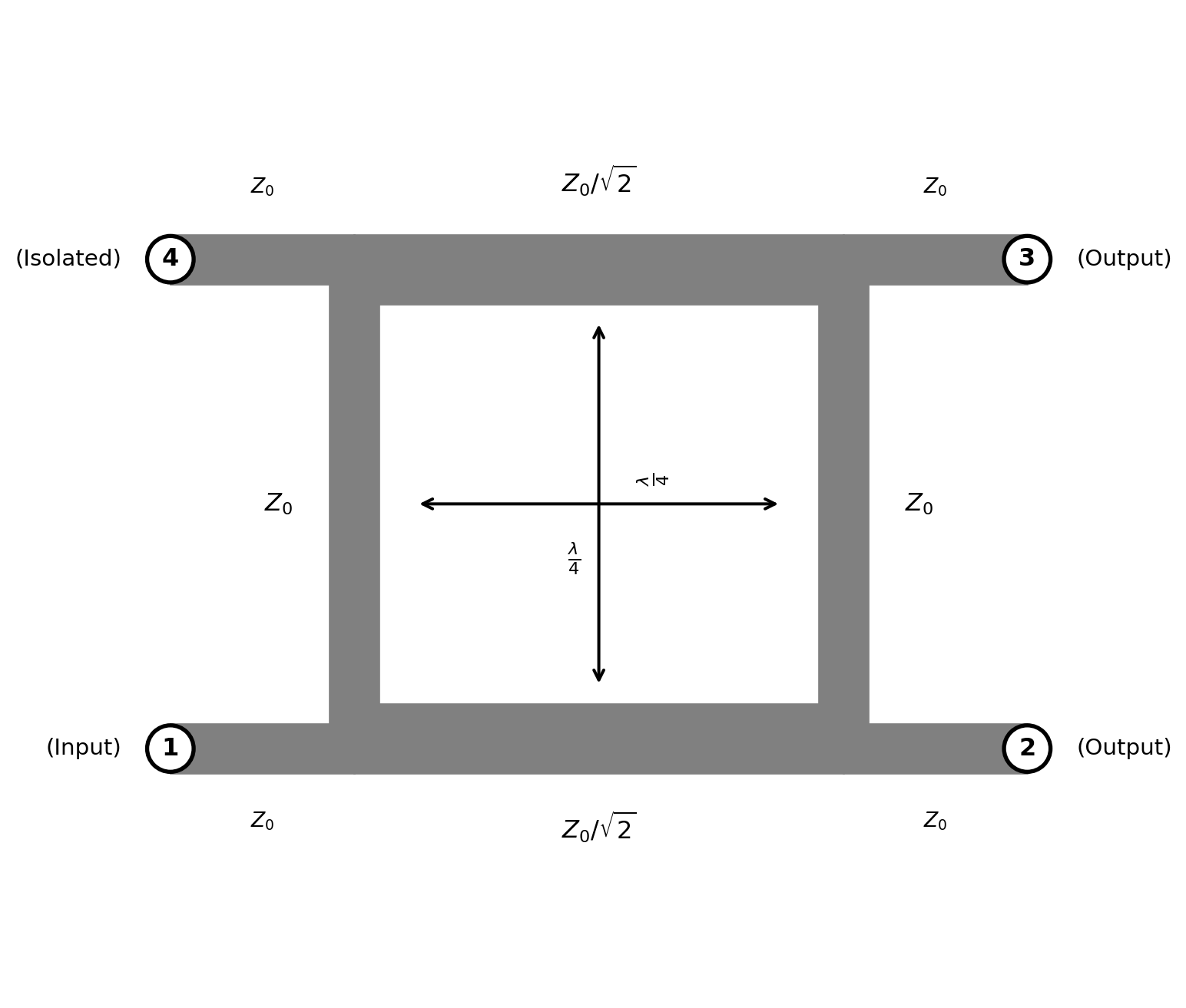
The 3-port S-parameter matrix of an ideal branch-line coupler (assuming port 4 is properly terminated with \(Z_0\)) is given by
\[ S = \frac{1}{\sqrt{2}} \begin{bmatrix} 0 & -j & -1 \\ -j & 0 & 0 \\ -1 & 0 & 0 \end{bmatrix}. \tag{49}\]
A feature of the coupler in Figure 57 is that it is single-ended; a differential implementation needs either two couplers or a coupler with subsequent baluns. An alternative implementation of a 90° hybrid coupler is the Lange coupler, which uses interdigitated fingers to achieve the required coupling. The Lange coupler can be implemented in a single-ended or differential way, and it can achieve very good performance over a wide frequency range. The disadvantage is that it requires a large number of fingers, which can take up a lot of area on-chip (Lange 1969).
Another approach, which is similar to the flip-flop based approach, is to use a delay line to generate the required phase shifts. This can be done with a single delay line and multiple taps, or with multiple delay lines. The idea is that we delay the input clock signal by a certain amount of time, which corresponds to a 90° phase shift at the target frequency. This approach is shown in Figure 58. Since the delay of a delay line is frequency dependent, and the delay will change with process, voltage, and temperature (PVT) variations, we have to implement a tuning mechanism to adjust the delay. This implementation is called a delay-locked loop (DLL), which is similar to a phase-locked loop (PLL, see Section 7).

With a phase detector (PD) we can compare the phase of the output signal with the input signal, and regulate the delay per stage so that after four delays the edges line up. Then we can tap the equally-spaced phases and use them as LO signals. The advantage of this approach is that we can flexibly create a required number of phases from an input clock. This feature is also used in wireline communication systems to generate multiple phases for the data sampling.
6 Oscillators
For the generation of the LO frequency to be used in a mixer for frequency conversion, oscillators are used. Ideally, oscillators produce a stable, noise-free sinusoidal signal, independent of environmental conditions like temperature or supply voltage variations. The circuit symbol of an oscillator is shown in Figure 59.

The question is how to construct an oscillator. In summary, we need to build something that oscillates, i.e., produces a sustained periodic signal with frequency \(\omega_0\). One way to achieve this is to construct a feedback loop where \(|H(s = j \omega_0)| = 1\) and \(\angle H(s = j \omega_0) = n \cdot 2 \pi\); these conditions are called the “Barkhausen criterion” (here, \(H(s)\) is the loop gain around the feedback loop). A ring oscillator is one example of such a feedback oscillator. For the 3-stage single-ended ring oscillator shown in Figure 60, each inverter provides a phase shift of \(2 \pi / 3\) at the oscillation frequency \(\omega_0\), resulting in a total phase shift of \(2 \pi\) for the three inverters. The gain condition is fulfilled by the gain of the inverters, which must be larger than unity to compensate for losses in the loop. By using an odd number of inverters, a stable locking point at dc is avoided.

Note that the output frequency of the ring oscillator shown above is ill-controlled, as it only depends on the delay (i.e., phase shift) of the inverters, which are usually dependent on process, voltage, and temperature (PVT) variations. Also, the inherent quality factor of such an oscillator is low, as exemplified by the definition of the quality factor \(Q\) as (Razavi 1996)
\[ Q = 2 \pi \frac{\text{Average energy stored}}{\text{Energy loss per cycle}} = \frac{\omega_0}{\Delta \omega} = \frac{\omega_0}{2} \sqrt{ \left( \frac{d A}{d \omega} \right)^2 + \left( \frac{d \varphi}{d \omega} \right)^2 } \tag{50}\]
with a ring oscillator having very low \(dA / d \omega\) and \(d \varphi / d \omega\) slopes (\(A(\omega)\) and \(\varphi(\omega)\) are the open loop gain and phase shift, respectively). It can be shown that \(Q \approx 1.3\) for a 3-stage ring oscillator (Razavi 1996). For some applications, this might be sufficient, but in many cases, a higher \(Q\) is desired to reduce phase noise and improve frequency stability (as we will see later in this chapter).
According to Equation 50, a high \(Q\) can be achieved by using a resonator with high energy storage capability and low energy loss per cycle. We then add an amplifier in a feedback loop to compensate for the losses of the resonator. This principle is shown in Figure 61 for a parallel LC tank circuit as the resonator. Sometimes the action of the feedback loop around the amplifier is modelled as a negative resistance \(-R_\mathrm{amp}\) that compensates for the losses of the tank circuit represented by the resistor \(R_\mathrm{p}\). The single parallel resistor \(R_\mathrm{p}\) models the losses of the inductor \(L\) and the capacitor \(C\).

When \(|-R_\mathrm{amp}| = R_\mathrm{p}\), the losses of the tank circuit are fully compensated, and we have a sustained oscillation at the resonance frequency \(\omega_0 = 1 / \sqrt{L C}\). In practice, the amplifier gain is usually set slightly higher than required for loss compensation to start the oscillation from noise. Then, as the oscillation amplitude increases, some non-linear mechanism in the amplifier reduces the effective gain until a stable oscillation amplitude is reached. Various implementations of such LC oscillators exist, which will be discussed in the following sections.
An alternative implementation of setting the oscillation amplitude is to use an automatic level control (ALC) loop, which measures the oscillation amplitude and adjusts the amplifier gain accordingly to maintain a constant output amplitude. This approach can improve the stability of the oscillation amplitude over process, voltage, and temperature variations.
An alternative to starting the oscillation from thermal noise (which can take considerable time depending on the \(Q\) of the resonator) is to provide a known initial condition to the resonator, e.g., by pre-charging the capacitor \(C\) to a certain voltage before enabling the amplifier. This way, the oscillation can start immediately from this initial energy stored in the resonator.
As a first hint on how to optimize an LC oscillator for low phase noise, we can try to maximize \(Q\) according to Equation 50. The energy stored in the capacitor at peak voltage is
\[ E_\mathrm{stored} = \frac{C V_\mathrm{osc,p}^2}{2} \]
so to maximize this we should maximize both \(C\) and the peak oscillation voltage \(V_\mathrm{osc,p}\). On the other hand, the energy loss per cycle is related to the power dissipated in the resistor \(R_\mathrm{p}\) by
\[ E_\mathrm{loss} = \frac{V_\mathrm{osc,p}^2}{2 R_\mathrm{p}} \cdot \frac{1}{f_0} \]
which we can minimize by maximizing \(R_\mathrm{p}\). In summary, to maximize \(Q\) we should use a large capacitance \(C\), a high oscillation amplitude \(V_\mathrm{osc,p}\), and a high tank resistance \(R_\mathrm{p}\). Note that increasing \(C\) will reduce \(L\) for a given \(\omega_0\). Calculating \(Q\) from these expressions yields
\[ Q = 2 \pi \frac{E_\mathrm{stored}}{E_\mathrm{loss}} = \omega_0 C R_\mathrm{p} \]
which confirms the above observations.
Fundamentally, if we describe the output voltage of the oscillator as
\[ v_\mathrm{osc}(t) = V_\mathrm{osc,p}(t) \cdot \cos[ \omega_0(t) t + \varphi(t) ] \]
we want to keep the amplitude variations small, i.e., \(V_\mathrm{osc,p}(t) = V_\mathrm{osc,p}\), and also the frequency variations small, i.e., \(\omega_0(t) = \omega_0\). We further want to minimize any phase fluctuations, i.e., \(\varphi(t) = \varphi_0\).
As a side note, the definition of \(Q\) in Equation 50 can also be understood as describing how many oscillation cycles it takes until the energy stored in the resonator is dissipated. For example, if \(Q = 1000\) at \(f_0 = 1\,\text{GHz}\), the energy stored in the resonator will last for approximately 1000 cycles, which is 1 µs. This time duration is sometimes called the “ring-down time” of the resonator.
6.1 Oscillator Noise
For calculating the noise of an oscillator, we assume that an LC-based oscillator as shown in Figure 61 is used. We assume that the oscillator is in steady-state operation, i.e., \(-R_\mathrm{amp} = R_\mathrm{p}\). We can then simplify the circuit to the one shown in Figure 62.

We can calculate
\[ Z_\mathrm{tank}(s) = \frac{s L \frac{1}{s C}}{s L + \frac{1}{s C}} = \frac{s L}{1 + s^2 L C}. \]
At \(s = j \omega_0\), we have \(Z_\mathrm{tank}(s) \to \infty\), so let’s approximate around \(\omega_0\):
\[ Z_\mathrm{tank}(j \omega_0 + j \Delta \omega) =\frac{j (\omega_0 + \Delta \omega) L}{1 - (\omega_0 + \Delta \omega)^2 L C} \]
For \(\Delta \omega \ll \omega_0\), we can approximate \((\omega_0 + \Delta \omega)^2 \approx \omega_0^2 + 2 \omega_0 \Delta \omega\) and \(\omega_0 + \Delta \omega \approx \omega_0\), which yields (using \(\omega_0^2 L C = 1\))
\[ Z_\mathrm{tank}(j \omega_0 + j \Delta \omega) = -\frac{j}{2 \Delta \omega C}. \]
We now use the correspondence \(C = 1 / \omega_0^2 L\) and express \(L = R_\mathrm{p} / \omega_0 Q\) to get
\[ |Z_\mathrm{tank}(j \omega_0 + j \Delta \omega)| = \frac{R_\mathrm{p}}{2 Q} \left( \frac{\omega_0}{\Delta \omega} \right) \]
which provides us with an expression for the magnitude of the tank impedance around resonance. We now calculate the noise power if a noise current is injected into this impedance. We use the single-sided noise current of \(R_\mathrm{p}\) (see Section 2.3.1), increased by a factor \(F\) contributed by the active circuit providing \(-R_\mathrm{amp}\):
\[ \overline{I_n^2} = \frac{4 k T F}{R_\mathrm{p}} \]
The noise voltage across the tank at a frequency offset \(\Delta \omega\) from \(\omega_0\) is then
\[ \overline{V_n^2}(\Delta \omega) = |Z_\mathrm{tank}(j \omega_0 + j \Delta \omega)|^2 \cdot \frac{4 k T F}{R_\mathrm{p}} = \frac{k T F R_\mathrm{p}}{Q^2} \left( \frac{\omega_0}{\Delta \omega} \right)^2 \]
This absolute noise voltage is not of much interest per se. We normalize it to the oscillation amplitude \(V_\mathrm{p}\), and only account for 1/2 of the noise, as the total noise power is split equally into amplitude noise and phase noise (Razavi 1996), and we are only interested in the phase noise. This is because we assume the amplitude noise is removed by amplitude clipping in the LO chain routing the oscillator signal to the mixer. This is often a valid assumption. We introduce the symbol \(\mathcal{L}\left\{\cdot\right\}\) to denote this normalized phase noise of the oscillator:
\[ \mathcal{L}\left\{\Delta \omega\right\} = \frac{\frac{1}{2} \frac{k T F R_\mathrm{p}}{Q^2} \left( \frac{\omega_0}{\Delta \omega} \right)^2}{\left( \frac{V_\mathrm{p}}{\sqrt{2}} \right)^2} = \frac{k T F R_\mathrm{p}}{V_\mathrm{p}^2} \cdot \frac{1}{Q^2} \cdot \left( \frac{\omega_0}{\Delta \omega} \right)^2 \tag{51}\]
This equation is known as “Leeson’s equation” (Leeson 1966), and it provides us with important insights on how to design low phase noise oscillators:
- Use a resonator with high quality factor \(Q\) to reduce phase noise. On-chip LC tanks usually provide moderate \(Q\) values (e.g., 10 to 30), while off-chip crystals can provide very high \(Q\) values (e.g., 10,000 to 100,000).
- Maximize the oscillation amplitude \(V_\mathrm{p}\) to increase the stored energy in the resonator. In CMOS implementations, this is often limited by the supply voltage and/or device breakdown voltages.
- Use an active circuit with low noise factor \(F\) to minimize the noise contribution of the negative resistance \(-R_\mathrm{amp}\). A good value to aim for is \(F \approx 2\) or lower.
- Maximize the tank resistance \(R_\mathrm{p}\) to minimize the thermal noise contribution. This can be achieved by using high-Q inductors and low-loss capacitors.
The phase noise \(\mathcal{L}\left\{\Delta \omega\right\}\) is expressed in the unit of dBc/Hz, i.e., in decibels of phase noise relative to the carrier power per 1 Hz of bandwidth. When expressing the phase noise of an oscillator in dBc/Hz it is important to state both the oscillation frequency \(\omega_0\) and the offset frequency \(\Delta \omega\) at which the phase noise is evaluated. For example, we could say that an oscillator has a phase noise of -137 dBc/Hz at 3 MHz offset from a carrier frequency of 2 GHz.
The phase noise expressed with Equation 51 describes an important region of the total oscillator phase noise where the phase noise decreases with \(1 / (\Delta \omega)^2\), i.e., with 20 dB per decade. This region is often called the “thermal noise region” as it is dominated by thermal noise from the tank resistor and the active circuit. However, at lower offset frequencies, other noise mechanisms (like flicker noise) can dominate, leading to different slopes of the phase noise vs. offset frequency curve. At larger offset frequencies, the phase noise can flatten out due to thermal noise floor limitation of buffer amplifiers following the oscillator. A typical phase noise plot of an LC oscillator is shown in Figure 63.
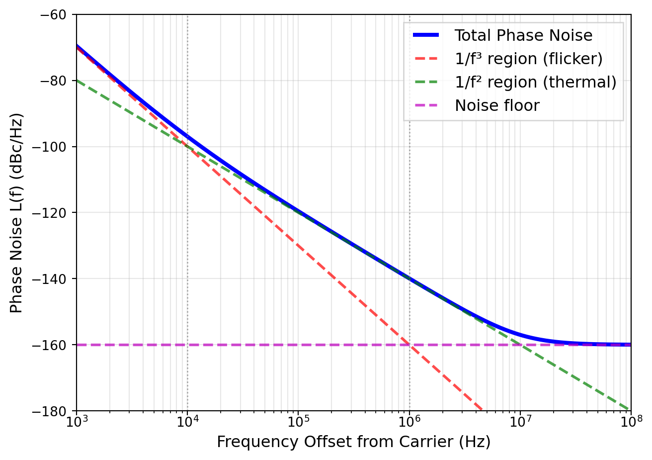
It is important to note that the phase noise does not go to infinity as \(\Delta \omega\) approaches zero, as Equation 51 might suggest. This is an artifact of the simplified model used to derive Leeson’s equation. In reality, the phase noise has the form of a Lorentzian spectrum around the carrier frequency, which means that it flattens out at very low offset frequencies with a trend described by
\[ \mathcal{L}\left\{\Delta \omega \ll\right\} \propto \frac{1}{\omega_\mathrm{B}^2 + \Delta \omega^2} \]
with \(\omega_\mathrm{B}\) being the half-power bandwidth of the oscillator spectrum.
Why is phase noise important?
- In RX and TX, the phase noise of the LO creates jitter, which degrades signal quality and contributes to EVM degradation.
- In TX, phase noise of the LO creates noise sidebands around the carrier, which can lead to adjacent channel interference together with spectral regrowth due to nonlinearities and thermal noise.
- In RX, reciprocal mixing of the phase noise sidebands of the LO with strong adjacent channel signals creates in-band noise, which degrades the SNR and sensitivity of the RX.
- In systems using multiple carriers or carriers with high-order modulation schemes (like in OFDM), phase noise can lead to inter-carrier interference (ICI) and symbol misinterpretation, further degrading system performance.
Note 7: Phase Noise and Frequency Division
When using a frequency divider to generate a lower-frequency LO signal from a higher-frequency oscillator (e.g., to generate IQ phases), the phase noise of the divided signal is affected by the division ratio \(N\) (Da Dalt and Sheikholeslami 2018). Specifically, the phase noise of the divided signal improves by \(20 \log_{10}(N)\) dB compared to the original oscillator phase noise. This means that if you divide the frequency by a factor of 2, the phase noise will be lowered by 6 dB!
The statement above is related to the phase noise at the output coming from the input of the divider. Of course, the frequency divider itself also contributes some additional phase noise, which can degrade the overall phase noise performance. However, in many practical cases, the improvement due to frequency division outweighs the additional noise introduced by the divider.
6.2 Jitter
Jitter is a time-domain representation of phase noise. It quantifies the timing variations of a periodic signal, such as the zero-crossings or rising edges of a clock signal. Jitter is typically measured in seconds (or fractions thereof) and can be expressed as root mean square (RMS) jitter or peak-to-peak jitter. The relationship between phase noise and RMS jitter can be approximated by the following equation (Da Dalt and Sheikholeslami 2018): \[ \sigma_\mathrm{a} = \frac{1}{2 \pi f_0} \sqrt{2 \int_{f_1}^{f_2} \mathcal{L}\left\{f\right\} df} \tag{52}\]
where \(\sigma_\mathrm{a}\) is the absolute RMS jitter, \(f_0\) is the carrier frequency, and the integral is taken over the frequency offset range from \(f_1\) to \(f_2\). This equation shows that higher phase noise levels lead to increased jitter, which can adversely affect the performance of digital communication systems by causing timing errors and signal integrity issues. Note that the phase noise \(\mathcal{L}\left\{f\right\}\) in Equation 52 must be expressed in linear scale (not dBc/Hz) when using this equation.
6.3 Reciprocal Mixing
Reciprocal mixing is a phenomenon that occurs in receivers when the phase noise sidebands of the local oscillator mix with strong adjacent channel signals, resulting in in-band noise that degrades the signal-to-noise ratio of the desired signal. This effect is particularly pronounced in systems with high-order modulation schemes or closely spaced channels, where even small amounts of phase noise can lead to significant performance degradation.
To analyze reciprocal mixing, we consider a scenario where a strong interferer is present at a frequency offset \(\Delta f\) from the desired signal. The phase noise of the local oscillator at this offset frequency can be characterized by its power spectral density \(\mathcal{L}\left\{\Delta f\right\}\). When the local oscillator mixes with the interferer, the phase noise sidebands effectively “fold” into the desired signal band, creating additional noise. This noise level can be estimated by multiplying the power of the interferer by the phase noise level at the offset frequency and considering the channel bandwidth \(B\) of the RX
\[ P_\mathrm{RM} = P_\mathrm{interferer} + \mathcal{L}\left\{\Delta f\right\} + 10 \log_{10}(B) \tag{53}\]
where \(P_\mathrm{RM}\) is the power of the reciprocal mixing noise introduced into the desired signal band.
Note 8: Reciprocal Mixing Example
Let us assume the following example from a Bluetooth LE receiver: The sensitivity target for the RX is -70 dBm with an SNR of 10 dB for a 1 MHz channel. An adjacent channel interferer is present at -27 dB channel to interferer ratio at an offset of 3 MHz. How much phase noise can the LO have to meet the sensitivity target?
From the sensitivity target and the SNR requirement, we can calculate the maximum allowable noise floor in the RX. We add a margin of 3 dB to account for implementation losses:
\[ \begin{split} P_\mathrm{noise,max} &= P_\mathrm{sens} - \text{SNR} - P_\mathrm{margin} \\ &= -70\,\text{dBm} - 10\,\text{dB} - 3\,\text{dB} = -83\,\text{dBm} \end{split} \]
The interferer power is:
\[ \begin{split} P_\mathrm{interferer} &= P_\mathrm{sens} - \text{C/I} \\ &= -70\,\text{dBm} + 27\,\text{dB} = -43\,\text{dBm} \end{split} \]
Using Equation 53, we can express the maximum allowable phase noise at 3 MHz offset at 2.4 GHz as:
\[ \begin{split} \mathcal{L}\left\{3\,\text{MHz}\right\} &= P_\mathrm{noise,max} - P_\mathrm{interferer} - 10 \log_{10}(B) \\ &= -83\,\text{dBm} + 43\,\text{dBm} - 60\,\text{dB} = -100\,\text{dBc/Hz} \end{split} \]
The reciprocal mixing scenario described in Note 8 is visualized in Figure 64.
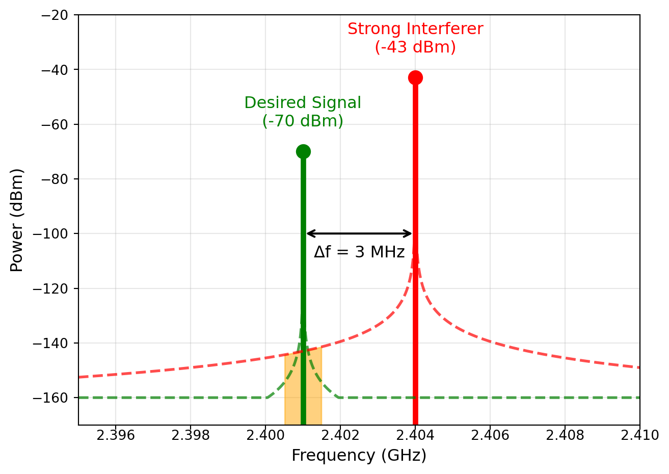
6.4 Single-Ended Oscillators
Single-ended oscillators are commonly used in RF applications due to their simplicity and ease of integration, especially in quartz oscillators. A negative resistance is implemented using a single transistor amplifier as is shown in Figure 65. The transistor is configured with two capacitors \(C_1\) and \(C_2\) to provide a phase-shifted feedback path.

It can be shown that the differential input impedance looking into the transistor gate and drain is given by
\[ Z_\mathrm{in}(s) = -\frac{g_\mathrm{m}}{\omega^2 C_1 C_2} + \frac{C_1 + C_2}{s C_1 C_2} = -R_\mathrm{amp} + \frac{1}{s C_\mathrm{amp}} \]
which consists of the series combination of a negative resistance \(-R_\mathrm{amp}\) and a capacitance \(C_\mathrm{amp}\). Note that the circuit in Figure 65 does not show a ground symbol. In fact, any of the three nodes marked with blue numbers can be used as a reference node (ground), and this results in the following well-known oscillator topologies:
| Reference Node | Oscillator Topology |
|---|---|
| Node 1 (Gate) | Colpitts oscillator |
| Node 2 (Source) | Pierce oscillator |
| Node 3 (Drain) | Clapp oscillator |
When we investigate the equivalent electrical circuit of a quartz crystal, we find that it has inductive behavior between its series resonance frequency and its parallel resonance frequency, which are very close together. The quartz crystal equivalent circuit is shown in Figure 66.

This means we can operate the quartz crystal as a high-Q inductor in an oscillator circuit, which results in the single-ended quartz crystal oscillator shown in Figure 67, which is a very popular choice for high-performance crystal oscillators. Note that in a simple implementation the current-bias MOSFET can be replaced by an inverter stage biased in the linear region.

The series combination of \(C_1\) and \(C_2\) provides the load capacitance required by the crystal to oscillate at its specified frequency. The oscillation frequency can be approximated by (\(C_\mathrm{load}^{-1} = 1/C_1 + 1/C_2\)):
\[ f_0 \approx \frac{1}{2 \pi \sqrt{L_\mathrm{m} C_\mathrm{load}}} \]
6.5 Differential Oscillators
After discussing single-ended oscillators in Section 6.4, we now turn to differential oscillator topologies, which are widely used in integrated LC oscillators due to their superior common-mode noise rejection and reduced even-order harmonics. A popular way to create a differential negative resistance is to use a cross-coupled pair of transistors as shown in Figure 68.

We assume a symmetrical circuit by setting \(g_\mathrm{m1} = g_\mathrm{m2} = g_\mathrm{m}\). By analyzing the small-signal equivalent circuit, we can derive the differential input impedance looking into the gates of the transistors:
\[ Z_\mathrm{in} = -\frac{2}{g_\mathrm{m}} \]
A practical implementation of a differential LC oscillator using the cross-coupled pair is shown in Figure 69 using a so-called “NMOS core”, as it is using an NMOS-based differential pair.

By putting the circuit in Figure 69 on its head, we obtain a “PMOS core” oscillator, which is also widely used in integrated LC oscillators. This configuration is shown in Figure 70.

In both oscillator topologies, the oscillation frequency is determined by the LC tank circuit formed by \(L = L_1 + L_2\) and \(C\). The oscillation frequency can be approximated by
\[ f_0 = \frac{1}{2 \pi \sqrt{L C}} \]
As both topologies have their inductor center tap tied to a supply rail (\(V_\mathrm{DD}\) for the NMOS core, \(V_\mathrm{SS}\) for the PMOS core), the voltage swing across the tank can go well beyond the supply voltage, which is an advantage of these topologies. However, note that the maximum voltage swing is still limited by the device breakdown voltages of \(M_1\) and \(M_2\), which can be critical in advanced CMOS technologies with low breakdown voltages. To utilize both an NMOS and a PMOS cross-coupled pair in parallel, a so-called “complementary (or CMOS) LC oscillator” can be used, which is shown in Figure 71. Here, the voltage swing across the tank is limited to the supply voltage, so it is inherently safe regarding device breakdown. Also, the transconductance of both NMOS and PMOS devices contributes to the negative resistance, which can reduce power consumption for a given oscillation amplitude.

Note that no bias current sources are shown in Figure 71, but can be added in practice. However, they require some voltage headroom, which lowers the maximum voltage swing across the tank, which is negative for phase noise performance according to Leeson’s equation in Equation 51.
The inductor \(L\) used in LC tanks is often implemented as a differential spiral inductor, which can be realized on-chip using the top metal layers of the CMOS process. If higher \(Q\) is sought, then off-chip inductors must be used, which is more expensive and uses package pins to connect the inductor. Alternatively, bondwire inductors can be used, which utilize the bondwires connecting the die to the package leads as inductors. Bondwire inductors can provide high \(Q\) values and are a cost-effective solution for improving oscillator performance without requiring off-chip components. For mm-wave frequencies, transmission line stubs can be used as inductors, which can be implemented on-chip using coplanar waveguide (CPW) or microstrip structures.
6.6 Frequency Tuning of Oscillators
Note that all three LC oscillator topologies shown in Section 6.5 have a fixed oscillation frequency determined by the LC tank circuit. In practice, it is often desirable to be able to tune the oscillation frequency over a certain range. There are only two ways to achieve this, either by tuning the inductance \(L\) or the capacitance \(C\) of the tank circuit. In integrated LC oscillators, it is common to use a fixed inductor and a tunable capacitor, which is shown in Figure 69, Figure 70, and Figure 71.
The need to change the oscillator frequency can arise from various requirements:
- We need to precisely tune the oscillator frequency to match a desired carrier frequency.
- The oscillator frequency needs to be adjusted to compensate for process, voltage, and temperature (PVT) variations that can affect the resonant frequency of the LC tank.
In order to achieve a tunable capacitance, a so-called “varactor” (variable capacitor) is often used. A varactor is a semiconductor device that exhibits a capacitance that varies with the applied voltage. Common ways to implement a varactor in integrated circuits are:
- Use the gate-to-channel capacitance of a MOSFET operated in reverse bias. By changing the voltage applied to the gate, the depletion region width in the channel changes, which in turn changes the capacitance.
- Use a PN-junction diode operated in reverse bias. The depletion region width of the diode changes with the applied voltage, leading to a change in capacitance.
- Use the gate-to-channel capacitance of a special MOSFET structure in accumulation mode, which can be achieved by using an NMOS situated in an n-well (in contrast to the usual operation in a p-well). Changing the gate-to-channel voltage changes the accumulation capacitance (Andreani and Mattisson 2000).
- Use a switched capacitor bank, where multiple capacitors are connected in parallel or series using switches (usually MOSFETs) to achieve discrete capacitance values.
In order to characterize the tuning sensitivity of an oscillator, the metric \(K_\mathrm{VCO}\) (voltage-controlled oscillator gain) is often used, which is defined as
\[ K_\mathrm{VCO} = \frac{d f_0}{d V_\mathrm{tune}} \]
with \(V_\mathrm{tune}\) being the control voltage applied to the varactor. The unit of \(K_\mathrm{VCO}\) is usually expressed in MHz/V or GHz/V. A high \(K_\mathrm{VCO}\) means that a small change in tuning voltage results in a large change in oscillation frequency, which can be beneficial for wide tuning ranges but can also make the oscillator more sensitive to noise on the tuning voltage line.
Note that the tuning sensitivity \(K_\mathrm{VCO}\) is usually quite nonlinear over the tuning range, so it is common to specify \(K_\mathrm{VCO}\) at a certain operating point or as an average value over the tuning range.
In order to achieve a wide tuning range while maintaining a sufficiently small \(K_\mathrm{VCO}\) for phase noise reasons, a combination of coarse and fine tuning mechanisms can be used (Kral et al. 1998). For example, a switched capacitor bank can provide coarse tuning steps, while a varactor can provide fine tuning within each step. It is important to ensure that the overall tuning range is free of dead zones, where the oscillator cannot be tuned to certain frequencies due to non-overlapping tuning ranges of the coarse and fine tuning elements.
While there are many ways to implement a switched capacitor for use in an oscillator tuning circuit, one popular way is shown in Figure 72. Many such switched capacitors with different values of \(C\) (often binary weighted) can be combined to form a capacitor bank for coarse frequency tuning.

Here, when the control signal \(S\) is high, the effective capacitance is \(C/2\), with a parasitic series resistance \(R_\mathrm{on}\) due to the switch. When \(S\) is low, the effective capacitance is \(C_\mathrm{off}\), which is the parasitic drain-source capacitance of the MOSFET switch.
Note that there exists a trade-off when designing the switched capacitor: A larger switch (with increased \(W\)) reduces \(R_\mathrm{on}\), but increases \(C_\mathrm{off}\). A large \(R_\mathrm{on}\) leads to increased losses in the tank circuit, which degrades the quality factor \(Q\) and increases phase noise according to Equation 51. On the other hand, a large \(C_\mathrm{off}\) reduces the effective tuning range of the switched capacitor, which can be detrimental if a wide tuning range is required.
In digitally-controlled oscillators (DCOs), the tuning voltage \(V_\mathrm{tune}\) is replaced by a digital control word that selects different capacitance values from a capacitor bank. This approach allows for precise and repeatable frequency tuning, which is beneficial in applications requiring frequency synthesis or channel selection. These fine tuning steps can also be implemented according to Figure 72; however, the value of \(C\) must be sufficiently small.
6.7 Oscillator Modelling
The instantaneous frequency of an oscillator can be expressed as
\[ \omega_\mathrm{VCO}(t) = \omega_0 + K_\mathrm{VCO} \cdot V_\mathrm{tune}(t) \]
where \(\omega_0\) is the nominal oscillation frequency, \(K_\mathrm{VCO}\) is the tuning sensitivity, and \(V_\mathrm{tune}(t)\) is the tuning voltage applied to the varactor. Looking at the instantaneous phase \(\varphi_\mathrm{VCO}(t)\) of the oscillator, we can integrate the instantaneous frequency \(\omega_\mathrm{VCO}(t)\) to obtain
\[ \varphi_\mathrm{VCO}(t) = \int_0^t \omega_\mathrm{VCO}(\tau) d\tau = \omega_0 t + K_\mathrm{VCO} \int_0^t V_\mathrm{tune}(\tau) d\tau. \]
Inspecting this equation, we see that with respect to phase, an oscillator is a perfect integrator of the tuning voltage over time! For simulation purposes, we can therefore model an oscillator as an integrator block as shown in Figure 73.

In this model we look at the phase output of the oscillator as an excess phase with respect to the nominal phase \(\omega_0 t\). This delta phase is obtained by integrating the tuning voltage \(V_\mathrm{tune}(t)\) scaled by \(K_\mathrm{VCO}\).
7 Phase-Locked Loops
Thinking about oscillators, we face a dilemma:
- Good phase noise performance is reached with high to very high \(Q\) in the resonator (see Equation 51).
- Oscillator tunability requires a tunable resonator, which usually results in a low-to-moderate \(Q\), unfortunately.
- Oscillators have inherent frequency stability issues due to temperature variations, device aging, and supply voltage fluctuations. However, for wireless communication systems, precise frequency control and a very stable LO (down to a few ppm of accuracy) are required.
7.1 Basic PLL Architecture
We solve the issues above by using a phase-locked loop (PLL) to stabilize and control the frequency of a tunable oscillator, mostly in the form of a VCO. A PLL is a feedback control system that locks the phase of the VCO output to the phase of a reference signal, typically generated by a crystal oscillator with excellent frequency stability. The block diagram of a basic PLL is shown in Figure 74.

The phase of a reference signal (often coming from a high-\(Q\) crystal oscillator) is compared to the phase of a VCO output signal in a phase detector (PD). The phase error is low-pass filtered and used to tune the VCO frequency. By continuously adjusting the VCO based on the phase difference, the PLL ensures that the VCO output remains synchronized with the reference signal, effectively combining the stability of the reference with the tunability of the VCO. When the output signal of the VCO is fed back to the phase detector through a frequency divider (with division ratio \(N\)), the PLL can generate output frequencies that are integer multiples of the reference frequency, given by \(f_\mathrm{out} = N \cdot f_\mathrm{ref}\).
The PD compares the phase of the reference signal with the phase of the VCO output signal. It works in the time domain and produces an output voltage proportional to the arrival time difference (phase difference) between the two input signals. This output voltage, known as the phase error signal, indicates whether the VCO is leading or lagging the reference signal in phase, expressed as
\[ \Delta \varphi = 2 \pi \frac{\Delta t}{T_\mathrm{ref}} \]
and
\[ V_\mathrm{error} = K_\mathrm{PD} \cdot \Delta \varphi \]
where \(\Delta \varphi\) is the phase difference (caused by the arrival time difference) in rad, \(K_\mathrm{PD}\) is the phase detector gain in V/rad, \(\Delta t\) is the time difference between the two signals, and \(T_\mathrm{ref}\) is the period of the reference signal.
An important consideration of the PD is its linear operating range. The PD can only provide a linear output voltage for small phase differences, typically within ±180° (±π rad). If the phase difference exceeds this range, the PD characteristic “wraps around,” leading to ambiguity in the phase error signal. This can cause the PLL to lose lock or behave unpredictably. Therefore, the PLL design must ensure that the phase difference remains within the linear range of the PD during normal operation, which is especially troublesome if the output frequency \(f_\mathrm{out}\) is not yet close enough to its final steady-state value. Note that a simple PD can be implemented by using an XOR gate for digital signals or a mixer for analog signals.

We can see in Figure 75 that the output of the XOR PD is high when the two input signals differ and low when they are the same. The output duty cycle is proportional to the phase difference between the two input signals. Note that this PD has no notion of frequency, only phase! Still, it can be used to lock the frequency of the VCO to the reference frequency, as a constant phase difference implies equal frequencies; however, this works only if the initial frequency difference is small enough. Also, this XOR-based PD does not evaluate the edges of the input signals, only their logic states. Therefore, it is crucial that both input signals are square waves with a 50% duty cycle to ensure proper operation of the PD.
NoteJK Flip-Flop Phase Detector
Instead of an XOR gate, which requires 50% duty cycle input signals, an edge-triggered JK flip-flop can be used. While the overall behavior is similar, the JK flip-flop-based PD is insensitive to duty cycle variations of the input signals, as it only evaluates the rising edges of the reference and feedback signals (Best 1999).
As the output signal of the PD contains high-frequency components (at least at twice the reference frequency), a low-pass filter (LPF) is used to smooth the phase error signal before it is applied to the VCO tuning input. The LPF also determines the dynamic response of the PLL, affecting its stability and transient behavior. A well-designed LPF ensures that the PLL can quickly respond to changes in the reference signal or disturbances while maintaining stability and minimizing overshoot or oscillations in the output frequency. Often, the LPF has voltage-mode inputs and outputs to connect to the PD and VCO, respectively.
Using a digital divider in the feedback path to only pass every \(N\)-th cycle of the VCO output to the PD allows the PLL to generate output frequencies that are integer multiples of the reference frequency. This is particularly useful in applications such as frequency synthesis, where a wide range of frequencies is required from a single stable reference source. By adjusting the division ratio \(N \in \mathbb{N}\), the PLL can produce various output frequencies while maintaining phase lock with the reference signal. However, note that the frequency resolution of the output frequencies \(\Delta f_\mathrm{out}\) is limited to integer multiples of the reference frequency!
Putting everything together into an \(s\)-domain block diagram, the PLL can be modeled as shown in Figure 76.

For the loop filter transfer function \(H(s)\), we assume a simple first-order low-pass filter with a cutoff frequency of \(\omega_\mathrm{LP} = 1 / T_\mathrm{LP}\) given by
\[ H_\mathrm{LP}(s) = \frac{1}{1 + s T_\mathrm{LP}}. \]
ImportantWhy Regulate Phase Instead of Frequency (PLL vs. FLL)?
Before we proceed, it is worth discussing why PLLs regulate the phase of the VCO output rather than its frequency directly. The reason lies in the relationship between phase and frequency: Frequency is the time derivative of phase. By controlling the phase, the PLL inherently controls the frequency as well. Additionally, even if the phase regulation has a steady-state phase error \(\varphi_\mathrm{err}\), the frequency error in steady state is zero, as can be appreciated when inspecting
\[ \omega_\mathrm{out}(t) = \frac{d \varphi_\mathrm{out}(t)}{dt} = \frac{d}{dt} \left[ N \cdot \varphi_\mathrm{ref}(t) + \varphi_\mathrm{err} \right] = N \cdot \frac{d \varphi_\mathrm{ref}(t)}{dt} = N \cdot \omega_\mathrm{ref}(t). \]
In principle, one could also design a frequency-locked loop (FLL) that compares the frequencies of the reference and VCO output signals directly (by, e.g., using counters); however, this usually results in non-zero frequency error in steady state. Nevertheless, FLLs are often used in combination with PLLs to improve acquisition time and robustness, especially in scenarios with large initial frequency offsets.
We now derive the closed-loop transfer function of the PLL from reference phase \(\varphi_\mathrm{ref}(s)\) to output phase \(\varphi_\mathrm{out}(s)\). First, we note that
\[ V_\mathrm{PD}(s) = K_\mathrm{PD} \left[ \varphi_\mathrm{ref}(s) - \frac{\varphi_\mathrm{out}(s)}{N} \right] \]
and
\[ \varphi_\mathrm{out}(s) = \frac{K_\mathrm{VCO}}{s} \cdot H_\mathrm{LP}(s) \cdot V_\mathrm{PD}(s) = \frac{K_\mathrm{VCO}}{s} \cdot \frac{1}{1 + s T_\mathrm{LP}} \cdot K_\mathrm{PD} \left[ \varphi_\mathrm{ref}(s) - \frac{\varphi_\mathrm{out}(s)}{N} \right]. \]
Note that this equation has one integrator \(1/s\) (which we can also see in Figure 76). We call PLLs with one integrator in the loop a Type-I PLL. We can now rearrange to find the closed-loop transfer function \(H(s)\) as
\[ H(s) = \frac{\varphi_\mathrm{out}(s)}{\varphi_\mathrm{ref}(s)} = N \cdot \frac{K_\mathrm{VCO} \cdot K_\mathrm{PD} \cdot \omega_\mathrm{LP} / N}{s^2 + s \cdot \omega_\mathrm{LP} + K_\mathrm{VCO} \cdot K_\mathrm{PD} \cdot \omega_\mathrm{LP} / N}. \tag{54}\]
We can use all techniques known from control theory to analyze the stability and dynamic response of the PLL based on Equation 54, however, we have to keep the following in mind:
- \(H(s)\) is a small-signal model of the PLL around its locked operating point, only valid for small perturbations. Large-signal behavior, such as acquisition and lock range, is not captured by this model.
- A PLL is a sampled system, working at instants of \(T_\mathrm{ref}\). \(H(s)\) is a continuous-time approximation, which is valid only if the loop bandwidth is much smaller (typically \(1/10\)) than the reference frequency \(f_\mathrm{ref}\). If this approximation is not valid, a discrete-time model of the PLL must be used, deriving the \(z\)-domain transfer function \(H(z)\).
If we compare the canonical form of a second-order system given by
\[ H(s) = N \cdot \frac{\omega_\mathrm{n}^2}{s^2 + s \cdot 2 \zeta \omega_\mathrm{n} + \omega_\mathrm{n}^2}, \]
with Equation 54, we can identify the natural frequency \(\omega_n\) and the damping factor \(\zeta\) of the PLL as
\[ \omega_\mathrm{n} = \sqrt{\frac{K_\mathrm{VCO} \cdot K_\mathrm{PD} \cdot \omega_\mathrm{LP}}{N}} \tag{55}\]
and
\[ \zeta = \frac{1}{2} \sqrt{\frac{\omega_\mathrm{LP} \cdot N}{K_\mathrm{VCO} \cdot K_\mathrm{PD}}}. \tag{56}\]
This allows us to use standard control theory results to design the PLL parameters \(K_\mathrm{PD}\), \(K_\mathrm{VCO}\), \(\omega_\mathrm{LP}\), and \(N\) to achieve the desired dynamic response and stability margins. Note that \(\omega_\mathrm{n}\) and \(\zeta\) are not independent, as they both depend on the same set of PLL parameters! This seriously limits the design of the loop dynamics and means that we need a more complex loop filter \(H_\mathrm{LP}(s)\) to achieve more freedom in selecting \(\omega_\mathrm{n}\) and \(\zeta\) independently. Often, we want to choose \(\zeta = 1/\sqrt{2} \approx 0.707\) to achieve a maximally-flat Butterworth response with minimal overshoot.
The poles of a second-order system are given by
\[ p_{1,2} = -\omega_\mathrm{n} \left( \zeta \pm \sqrt{\zeta^2 - 1} \right) \]
with \(\zeta = 1/\sqrt{2}\) resulting in complex conjugate poles at
\[ p_{1,2} = -\frac{\omega_\mathrm{n}}{\sqrt{2}} \pm j \frac{\omega_\mathrm{n}}{\sqrt{2}}. \]
To summarize: We can make a simple PLL using an XOR for a PD, use a first-order LPF, plus a feedback divider to get frequency multiplication of \(f_\mathrm{out} = N \cdot f_\mathrm{ref}\). However, the control over the loop dynamics is very limited, and the locking procedure of the PLL is tricky, as the PD has a limited linear range of ±180°, requiring that the VCO frequency at the start of the locking procedure is already close enough to the desired output frequency. In addition, \(N\) is an integer, limiting the frequency resolution of the output frequencies to integer multiples of the reference frequency.
The question is how to improve the PLL design to overcome these limitations. We will explore advanced PLL architectures and techniques in the following section.
7.2 Charge-Pump PLL
The fundamental limitations of the simple PLL architecture presented in Section 7.1 can be addressed by using a more sophisticated phase detector known as a phase-frequency detector (PFD) in combination with a charge pump (CP) (Gardner 1980). This combination allows for better control over the loop dynamics and improved locking behavior.
In order to drive the CP, we envision a PFD with two digital outputs: an “up” signal that indicates when the VCO phase lags behind the reference phase, and a “down” signal that indicates when the VCO phase leads the reference phase (Brown 1971). The PFD compares both the phase and frequency of the reference and feedback signals, providing a more robust locking mechanism. The typical implementation of a PFD is shown in Figure 77.

The PFD operates as follows:
- If the reference signal leads the feedback signal (its rising edge arrives first), the “UP” output is activated, causing the CP to source current into the integration capacitor, increasing the VCO tuning voltage and thus the VCO frequency.
- If the feedback signal leads the reference signal (its rising edge arrives first), the “DOWN” output is activated, causing the CP to sink current from the integration capacitor, decreasing the VCO tuning voltage and thus the VCO frequency.
- If both signals are aligned in phase and frequency, both outputs are only activated for a short time (the gate delays of the DFF and the AND), and the CP does not source or sink current; the integration capacitor in the loop filter holds its voltage, maintaining the VCO frequency.
- The rising edge that arrives last resets both outputs, ensuring that the CP only sources or sinks current for a duration proportional to the phase difference between the two signals.
In the following, we will look at four different cases of PFD operation to illustrate its behavior.
- Reference leads feedback: The “UP” output is activated, and the CP sources current to the loop filter, increasing the VCO frequency.

- Feedback leads reference: The “DOWN” output is activated, and the CP sinks current from the loop filter, decreasing the VCO frequency.

- Both signals aligned: Both outputs are briefly activated, but the CP does not source or sink current, maintaining the VCO frequency.

- Large frequency difference: The PFD continues to source or sink current until the phases align, allowing the PLL to acquire lock even with large initial frequency offsets.

Let us now investigate the circuit of the CP. The UP and DOWN signals from the PFD control two current sources/sinks connected to the loop filter capacitor, as shown in Figure 82.

When the UP signal is high, the CP sources a constant current \(I_\mathrm{CP}\) into the loop filter capacitor \(C_\mathrm{int}\), increasing its voltage linearly over time according to the phase error. Conversely, when the DOWN signal is high, the CP sinks a constant current \(I_\mathrm{CP}\) from the capacitor, decreasing its voltage linearly.
Note that the top and bottom current sources must be well matched to ensure symmetric operation of the CP and should have a wide operating range. The output impedance of the CP is ideally very high so that the charge pump current does not depend on the voltage across the loop filter capacitor. Further, the switches introduce charge injection and clock feedthrough, which can cause unwanted ripples on the loop filter voltage, leading to spurious signals in the PLL output. Careful design of the switches and careful layout techniques are necessary to minimize these effects.
The voltage change on the capacitor can be expressed as
\[ \Delta V_\mathrm{LF} = \frac{1}{C_\mathrm{int}} \int_0^{t_\mathrm{on}} I_\mathrm{CP} \cdot dt \tag{57}\]
where \(t_\mathrm{on}\) is the duration for which the UP or DOWN signal is active, proportional to the phase difference between the reference and feedback signals.
Taking the Laplace transform of Equation 57, we find the transfer function of the CP from the UP/DOWN control signals to the loop filter voltage as
\[ H_\mathrm{CP}(s) = \frac{I_\mathrm{CP}}{2 \pi} \left( \frac{1}{s C_\mathrm{int}} + R_\mathrm{int} \right) \tag{58}\]
where we have added a resistor \(R_\mathrm{int}\) in series with the capacitor \(C_\mathrm{int}\) to introduce a zero in the loop filter transfer function. The need for this zero will become apparent when we analyze the PLL loop dynamics next.
The resulting PLL using a PFD-CP combination is shown in Figure 83.

Neglecting \(C_3\) for now, we can derive the closed-loop transfer function of the PLL from reference phase \(\varphi_\mathrm{ref}(s)\) to output phase \(\varphi_\mathrm{out}(s)\) as
\[ H(s) = \frac{\varphi_\mathrm{out}(s)}{\varphi_\mathrm{ref}(s)} = N \cdot \frac{\frac{I_\mathrm{CP} K_\mathrm{VCO}}{2 \pi C_\mathrm{int} N} (1 + s C_\mathrm{int} R_\mathrm{int})}{s^2 + s \frac{I_\mathrm{CP} K_\mathrm{VCO} R_\mathrm{int}}{2 \pi N} + \frac{I_\mathrm{CP} K_\mathrm{VCO}}{2 \pi C_\mathrm{int} N}} = N \cdot \frac{s \cdot 2 \zeta \omega_\mathrm{n} + \omega_\mathrm{n}^2}{s^2 + s \cdot 2 \zeta \omega_\mathrm{n} + \omega_\mathrm{n}^2} \tag{59}\]
with
\[ \omega_\mathrm{n} = \sqrt{\frac{I_\mathrm{CP} K_\mathrm{VCO}}{2 \pi C_\mathrm{int} N}} \tag{60}\]
and
\[ \zeta = \frac{R_\mathrm{int}}{2} \sqrt{\frac{I_\mathrm{CP} K_\mathrm{VCO} C_\mathrm{int}}{2 \pi N}}. \tag{61}\]
Looking at Equation 60 and Equation 61, we can see that we now have one additional independent parameter (\(R_\mathrm{int}\)) to set the natural frequency \(\omega_\mathrm{n}\) and the damping factor \(\zeta\) of the PLL independently (compare this to Equation 55 and Equation 56). This allows us to design the loop dynamics more flexibly to achieve the desired performance.
With Equation 61, we can now appreciate the need for the resistor \(R_\mathrm{int}\) in series with the capacitor \(C_\mathrm{int}\) in the loop filter. Without this resistor, the damping factor \(\zeta\) would be zero, leading to an undamped system with oscillatory behavior and poor transient response. The resistor introduces a zero in the loop filter transfer function, providing the necessary damping to stabilize the PLL and improve its dynamic response.
Looking at Figure 83 and Equation 58, we can also see that the PFD-CP introduces another integrator in the loop. This integrator, together with the integrator from the VCO, makes the PLL a Type-II PLL. A Type-II PLL can achieve zero steady-state phase error for step changes in the reference phase and zero steady-state frequency error for ramp changes in the reference frequency.
In conclusion:
- The PLL regulates the phase of a VCO to match the phase of a reference signal, using feedback control. Even with a steady-state phase error, the frequency error is zero (Type-I PLL). In a Type-II PLL, both phase and frequency errors are zero in steady state.
- The lowpass behavior of the loop filter determines the dynamic response and stability of the PLL.
- Further, the PLL transfer function from reference phase to output phase has the form of a lowpass, which passes the reference oscillator phase noise to the output inside the passband. The phase noise of the VCO is suppressed inside the loop bandwidth, as the PLL corrects for phase deviations.
- Outside the PLL loop bandwidth, the VCO phase noise dominates, as the PLL cannot correct for phase deviations fast enough.
This phase noise shaping behavior is illustrated in Figure 84, which shows how the reference and VCO phase noise contributions combine to form the total PLL output phase noise.
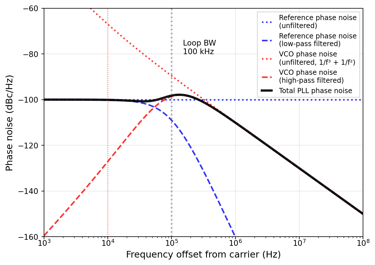
Note that inside the PLL loop bandwidth the reference phase noise is multiplied by \(N^2\) in power, i.e., \(20 \log_{10}(N)\) in dB, as the PLL output frequency is \(N\) times the reference frequency. In Figure 84, \(N = 100\) and a reference phase noise of -140 dBc/Hz is used. Large values of \(N\) can significantly increase the reference phase noise contribution at the PLL output, which is why low phase noise references are essential for high-performance PLLs.
7.3 All-Digital PLL
In the PLL implementations discussed so far, we have used analog components such as the VCO, loop filter, and charge pump. While these analog PLLs can achieve excellent performance, they also come with challenges such as component variability, temperature sensitivity, and integration complexity in modern digital processes. The question arises: Can we implement a PLL using only digital components to overcome these challenges? The answer is yes, leading to the concept of the all-digital phase-locked loop (ADPLL) (Staszewski et al. 2003), whose block diagram is shown in Figure 85.

Conceptually, the ADPLL in Figure 85 is similar to the analog PLL in Figure 74, with the key difference being that all components are implemented digitally. The phase detector is replaced by a time-to-digital converter (TDC), which measures the time difference between the reference and feedback signal edges and converts it into a digital phase error word. The loop filter is implemented as a digital filter (FIR, IIR, or similar), processing the phase error word to generate a tuning word for the digitally controlled oscillator (DCO). The DCO generates the output frequency based on the tuning word, completing the feedback loop.
The advantages of the ADPLL are that it can be fully integrated in a digital nm CMOS process, benefiting from scalability, low power consumption, small chip area, and immunity to analog component variations. Additionally, the digital nature of the ADPLL allows for easy programmability and adaptability to different applications. However, the ADPLL also faces challenges such as quantization noise from the TDC and DCO, nonlinearity (DNL and INL) of TDC and DCO, as well as coupling of digital switching noise into the oscillator output signal.
7.3.1 Time-to-Digital Converter
The TDC is a crucial component of the ADPLL, responsible for measuring the time difference between the reference and feedback signal edges and converting it into a digital phase error word. The TDC operates by sampling the time interval between two events (the rising edges of the reference and feedback signals) and quantizing this interval into discrete levels. TDCs can be implemented using various techniques. One popular method is using a digital delay line. An exemplary implementation is shown in Figure 86.

In Figure 86, the reference signal edge runs through a series of buffers (delay elements) connected in a delay line configuration. The feedback signal edge is used to sample the state of the delay line at the moment it arrives. The outputs of the DFFs represent the time difference between the reference and feedback signals, which can be encoded into a digital phase error word. The resolution of the TDC is determined by the delay between each stage in the delay line, with finer delays providing higher resolution. However, increasing the resolution also increases the complexity and power consumption of the TDC.
The phase noise of the TDC (at the output of the ADPLL) arising from this time measurement quantization can be modeled as
\[ \mathcal{L}\left\{f\right\} = 10 \cdot \log \left[ \frac{(2 \pi)^2}{12 f_\mathrm{ref}} \cdot \left( \frac{\Delta T_\mathrm{TDC}}{T_\mathrm{DCO}} \right)^2 \right] \]
where \(\Delta T_\mathrm{TDC}\) is the time resolution of the TDC, \(T_\mathrm{DCO}\) is the period of the DCO output frequency, and \(f_\mathrm{ref}\) is the reference frequency. This equation shows that improving the TDC resolution (reducing \(\Delta T_\mathrm{TDC}\)) and increasing the reference frequency can help reduce the phase noise contribution from the TDC.
NoteTDC Resolution Example
To get an idea of the performance requirements for the TDC, we assume a DCO output frequency of 2.4 GHz (e.g., for a Bluetooth application) and a reference frequency of 40 MHz. If we aim for a TDC phase noise contribution of -100 dBc/Hz at the DCO output, we can rearrange the above equation to find the required TDC time resolution:
\[ \Delta T_\mathrm{TDC} = T_\mathrm{DCO} \cdot \sqrt{\frac{12 f_\mathrm{ref} \cdot 10^{\mathcal{L}\left\{f\right\}/10}}{(2 \pi)^2}} = \frac{1}{2.4 \times 10^9} \cdot \sqrt{\frac{12 \cdot 40 \times 10^6 \cdot 10^{-10}}{(2 \pi)^2}} \approx 15\,\text{ps} \]
This number is challenging but achievable with modern TDC designs in nm CMOS.
7.3.2 Digitally Controlled Oscillator
With the implementation of the TDC clarified in Section 7.3.1, we now turn our attention to the digitally controlled oscillator (DCO), which generates the output frequency of the ADPLL based on a digital tuning word. The DCO is a digital equivalent of the VCO used in analog PLLs, and its frequency is adjusted by changing the digital input value. Fundamentally, two possible implementations exist:
- An analog-controlled oscillator (e.g., a VCO) is combined with a digital-to-analog converter (DAC) to convert the digital tuning word into an analog control voltage. This approach is shown in Figure 87.

- A digitally-controlled oscillator uses a large number of small varactors or switched capacitor banks to adjust the oscillation frequency directly based on the digital tuning word. An example implementation of a switched varactor is shown in Figure 88, or a switched capacitor like shown in Figure 72 is used.

It has to be noted that while an ADPLL seems conceptually simpler than an analog PLL, the design of high-performance TDCs and DCOs can be quite complex and requires careful consideration of quantization noise, linearity, and power consumption. Coupling effects between different circuit blocks can also introduce unwanted spurs and phase noise folding in the ADPLL output. Therefore, while ADPLLs offer many advantages, they also present unique design challenges that must be addressed to achieve adequate performance.
7.4 Fractional-N PLL
With the PLL architectures discussed so far, the output frequency resolution is limited to integer multiples of the reference frequency, i.e., \(f_\mathrm{out} = N \cdot f_\mathrm{ref}\) with \(N \in \mathbb{N}\). For a fine output frequency resolution, this requires a very low reference frequency. With the rule of thumb that the PLL loop bandwidth should be less than \(f_\mathrm{ref}/10\) to ensure stable operation, a low reference frequency also limits the achievable loop bandwidth, which is detrimental to phase noise performance and settling time. Further, we have learned in Section 7.2 that large values of \(N\) increase the reference phase noise contribution at the PLL output by \(20 \log_{10}(N)\) dB, making it challenging to achieve low phase noise performance with high frequency resolution.
How to break these fundamental limitations? The answer lies in the concept of the fractional-N PLL, which allows for non-integer frequency multiplication.
Assume we want to generate an output frequency of \(f_\mathrm{out} = 2.45\,\text{GHz}\) from a reference frequency of \(f_\mathrm{ref} = 40\,\text{MHz}\). This requires a frequency multiplication factor of \(N = 61.25\), which is not an integer. To achieve this, the fractional-N PLL employs a feedback divider that can switch between two integer division ratios, \(N_1\) and \(N_2\), such that the average division ratio over time equals the desired fractional value (the averaging is performed by the low-pass loop filter, providing the averaged tuning voltage to the VCO / the tuning word to the DCO). In this case, we can choose \(N_1 = 61\) and \(N_2 = 62\). By alternating between these two division ratios in a controlled manner, the PLL can effectively achieve an average division ratio of 61.25, allowing it to generate the desired output frequency of 2.45 GHz. The following sequence illustrates this concept over four reference cycles:
\[ N = N_1, N_1, N_1, N_2 \implies \text{Average } N = \frac{61 + 61 + 61 + 62}{4} = 61.25 \]
A simple sequence like the one above works, but would lead to significant spurs in the PLL output spectrum due to the periodic nature of the division ratio switching, especially when the fractionality is close to an integer, and thus the sequence is long. Consider the case of \(N = 61.01\), where we would need to switch to \(N_2 = 62\) only once every 100 cycles of \(N_1 = 61\):
\[ N = \frac{99 \cdot 61 + 1 \cdot 62}{100} = 61.01 \]
This periodic switching introduces spurious tones in the PLL output spectrum at multiples of \(f_\mathrm{ref}/100\), which can potentially pass through the loop filter and appear in the output spectrum, degrading the signal quality.
To minimize these spurs, more sophisticated techniques such as delta-sigma modulation are employed to randomize the switching sequence, spreading the quantization noise over a wider frequency range and reducing its impact on the PLL output. Additionally, the quantization noise introduced by the fractional division is pushed to higher frequencies where it can be more easily filtered out by the loop filter.
7.4.1 Delta-Sigma Modulator
For an in-depth understanding of delta-sigma modulation, we refer to (Schreier et al. 2017). Here, we briefly summarize the key concepts relevant to fractional-N PLLs. In a nutshell, a delta-sigma modulator (DSM) is a feedback system that shapes quantization noise to higher frequencies, allowing for high-resolution digital-to-analog conversion or frequency synthesis. The basic structure of a first-order DSM is shown in Figure 89.

In Figure 89, the input signal \(X(s)\) is transferred to the output \(Y(s)\) with the following transfer function (we set \(Q = 0\)):
\[ Y(s) = X(s) \cdot \frac{1}{1 + s T} = X(s) \cdot H_\mathrm{LP}(s) \]
The quantization noise \(Q(s)\) introduced by the quantizer is shaped by the feedback loop, resulting in the following output contribution:
\[ Y(s) = Q(s) \cdot \frac{s T}{1 + s T} = Q(s) \cdot H_\mathrm{HP}(s) \]
We can see that the quantization noise is highpass filtered, pushing it to higher frequencies, where it can be more easily filtered out by a subsequent lowpass filter.
The digital implementation of a first-order DSM is straightforward and one possible form is shown in Figure 90. At the point of truncation from \(N+2\) bits to 1 bit (the MSB) we imagine quantization noise \(q[n]\) being added to the signal.

Calculating the \(z\)-domain transfer functions from input \(X(z)\) to the output \(Y(z)\) (the signal transfer function, STF) and quantization noise \(Q(z)\) to \(Y(z)\) (the noise transfer function, NTF), we find
\[ \frac{Y(z)}{X(z)} = \text{STF}(z) = z^{-1} \]
and
\[ \frac{Y(z)}{Q(z)} = \text{NTF}(z) = (1 - z^{-1}) \implies \text{NTF} = 1 - z^{-1}. \]
We see that the STF is a simple delay, while the NTF has a zero at DC, pushing the quantization noise to higher frequencies. Evaluating the frequency response of the NTF to find the frequency-shaped PSD of the quantization noise, we find
\[ S_\mathrm{y}(f) = S_\mathrm{q}(f) |H(f)|^2 = S_\mathrm{q}(f) \cdot 2 \left| 1 - \cos(2 \pi f T_\mathrm{s}) \right| \implies H(f) = \sqrt{ 2 \left| 1 - \cos(2 \pi f T_\mathrm{s}) \right| }. \]
with \(T_\mathrm{s}\) being the sampling period of the DSM. The resulting \(H(f)\) is shown in Figure 91. With the assumed PLL loop bandwidth of 100 kHz and a reference frequency of 40 MHz, we can see that the quantization noise is significantly attenuated inside the PLL loop bandwidth, minimizing its impact on the PLL output phase noise. The general trend is that higher-order DSMs and faster sampling frequencies lead to better noise shaping and lower in-band quantization noise.
If we analyze the signal properties of the number sequence generated by the first-order DSM in Figure 90, we find that its randomization properties are not ideal, leading to spurs in the PLL output spectrum. To improve the randomization properties, higher-order DSMs are used in fractional-N PLLs, especially 2nd or 3rd order. A consequence of a higher-order DSM is that the produced sequence can take more values than just \(N\) and \(N+1\). The range of produced values is shown in Table 5.
| DSM Order | Output Range | Noise Shaping |
|---|---|---|
| 1 | \(N, N+1\) | 20 dB/decade |
| 2 | \(N-1 \ldots N+2\) | 40 dB/decade |
| 3 | \(N-3 \ldots N+4\) | 60 dB/decade |
A standard 3rd-order DSM implementation has issues with stability due to the phase shift of three integrators in the feedback loop. To mitigate this, a well-known architecture called the MASH (multi-stage noise shaping) DSM is often used (Matsuya et al. 1989), which consists of multiple first-order DSM stages cascaded together. An example Python implementation of a 3rd-order MASH DSM is shown in Figure 92, showing a snippet of the time-domain output and the resulting frequency spectrum, showing the noise shaping. As can be clearly seen, even using a 3rd-order MASH, there are strong spurious signals showing up in the spectrum. The time series shows that for some static input values (like here 0.125) patterns with a short period can exist.
As a potential solution, we can add a very small dithering signal (i.e., adding a random signal to the input), which breaks these patterns. As shown in Figure 93, dithering indeed causes enough randomization so that the noise shaping can be clearly seen without noticeable spurs (this is evident when comparing the time series of Figure 92 and Figure 93). Care has to be taken that the added random noise is small enough to not cause issues with in-band noise.
A block diagram of a 3rd-order MASH 1-1-1 implementation including dither injection (shown in blue) is depicted in Figure 94. The dither is typically implemented digitally as a pseudo-random bit sequence (PRBS) generator, often in the form of a linear-feedback shift register (LFSR).

7.4.2 Fractional-N PLL Implementation
A block diagram of a fractional-N PLL using a DSM and a multi-modulus divider (MMD) is shown in Figure 95. In order to ease the timing loop of the jittered clock coming from the MMD, the DSM is typically clocked by the MMD’s output.

For a practical implementation of a fractional-N PLL, it is of utmost importance that the path from the MMD output to the loop filter output is linear, as only the averaging/lowpass filtering of the noise-shaped quantization noise reduces the noise. Any nonlinearity in this path will lead to distortion of the quantization noise, causing quantization noise to fold back into the PLL loop bandwidth, degrading the PLL output phase noise!
One prominent source of nonlinearity is the difference between the source and sink currents of the charge pump, as well as any nonlinearity present in the PFD/CP operating point of \(\Delta \varphi \approx 0\) (like a deadzone). Since a Type-II PLL ideally operates at exactly this point, with random excursions around it due to the DSM-induced jitter, any nonlinearity here will seriously degrade the PLL performance. There are predominantly two options to mitigate this issue:
- Use a Type-I PLL architecture with \(\Delta \varphi \neq 0\).
- Introduce a phase offset in a Type-II PLL to operate away from \(\Delta \varphi = 0\).
A simple way to introduce a phase offset is to add a fixed current source/sink to the charge pump, as shown in Figure 96.

As we have seen multiple times in the PLL discussion, using a higher \(f_\mathrm{ref}\) is beneficial for phase noise performance, loop bandwidth, and TDC resolution (in an ADPLL). However, in many applications the choice of reference frequency is constrained by other factors. One way to achieve a higher reference frequency is by using a frequency doubler. As shown in Figure 97, a frequency doubler can be implemented using an XOR gate and a delay line. The delay line is set to a quarter of the period of the reference frequency, i.e., \(T_\mathrm{d} = T_\mathrm{ref} / 4\). The XOR gate then produces an output frequency of \(f_\mathrm{double} = 2 \cdot f_\mathrm{ref}\). For stable operation, this delay line must be designed to be relatively insensitive to process, voltage, and temperature (PVT) variations, or must be adjusted with a control loop.

As a final remark, we note that the output of the MMD in Figure 95 is a jittered clock due to the changing division ratio and the multiple gates and flip-flops that make up the MMD. This jitter degrades the PLL phase noise performance. Fortunately, there is an easy fix for this issue by using a retiming flip-flop after the MMD, clocked by the oscillator output, as shown in Figure 98.

This retiming flip-flop effectively synchronizes the MMD output to the oscillator clock domain, significantly reducing the jitter seen by the loop filter and improving the overall phase noise performance of the fractional-N PLL.
8 Power Amplifiers
Power amplifiers (PAs) are essential components in wireless communication systems, as they boost the signal power from (usually) a few milliwatts up to several watts to ensure reliable transmission over the air. While PAs are simple in concept, their design and operation involve several trade-offs between efficiency, linearity, bandwidth, and cost.
A basic PA based on a single common-source stage is shown in Figure 99. The input signal is applied to the gate of the transistor via an input matching network. The transistor amplifies the signal at the drain terminal, and the output matching network transforms the \(50\,\Omega\) load to the optimal load impedance for the desired output power under linearity and efficiency constraints.

The RF choke at the drain allows the drain node to swing above the supply voltage, enabling higher output power. However, the transistor \(M_1\) must be able to handle the high voltages and currents involved. Unfortunately, in silicon technologies the Johnson limit, which is the product of the breakdown voltage and the transit frequency of the transistor, is limited to around 200 GHz·V. This often requires the use of different semiconductor technologies for the PAs, such as GaAs, InP, or GaN. Implementing the PA in a different technology than the rest of the RFIC means implementing it off-chip.
Assuming the output voltage swing is limited only by the supply voltage \(V_\mathrm{DD}\), the maximum output power delivered to a load \(R_\mathrm{L}\) is given by
\[ P_\mathrm{out,max} = \frac{V_\mathrm{DD}^2}{2 R_\mathrm{L}}. \]
For a typical supply voltage of \(V_\mathrm{DD} = 3\,\mathrm{V}\) and a load of \(R_\mathrm{L} = 50\,\Omega\), this results in a maximum output power of \(P_\mathrm{out,max} = 90\,\mathrm{mW}\) or \(19.5\,\mathrm{dBm}\). Higher output powers require either higher supply voltages (which may not be available in battery-powered systems) or lower load impedances. The output matching network is thus designed in such a way as to present a lower impedance to the PA, e.g., \(R_\mathrm{L} = 5\,\Omega\), which increases the maximum output power to \(P_\mathrm{out,max} = 900\,\mathrm{mW}\) or \(29.5\,\mathrm{dBm}\). The matching networks are usually implemented as LC networks or transmission line sections, often using transformers to achieve the required impedance transformation.
In order to drive the large output transistor \(M_1\) in Figure 99, a driver stage is often required. This driver stage provides the necessary voltage and current gain to ensure that the PA operates in its optimal region. If needed, even another pre-driver stage can be added, but higher gain might cause stability issues and increased output noise. A two-stage power amplifier is shown in Figure 100.

8.1 PA Efficiency
One of the main characteristics of a PA is its drain efficiency, which is defined as the ratio of the output RF power to the total DC power consumed from the supply:
\[ \eta = \frac{P_\mathrm{out}}{P_\mathrm{dc}} \]
Since \(\eta\) does not take into account the required input power to drive the PA, a more comprehensive metric is the power-added efficiency (PAE):
\[ \text{PAE} = \frac{P_\mathrm{out} - P_\mathrm{in}}{P_\mathrm{dc}} \]
Ideally, we want both efficiency metrics as high as possible, but in practice there is a trade-off between efficiency and linearity (for linearity metrics refer to Section 2.2). High efficiency is often achieved by operating the PA in saturation, which leads to signal distortion and spectral regrowth. Various techniques exist to improve the linearity of PAs, such as predistortion, feedback, and envelope tracking.
8.2 PA Nonlinearity
For describing PA nonlinearity, various models can be used. One simple model is the Saleh model (originally developed for traveling-wave tube amplifiers), which describes the AM/AM and AM/PM conversion of the PA using a smooth transition from linear operation to saturation (Saleh 1981). This model is defined by the following equations in the polar domain (\(r(t)\) and \(\psi(t)\) are the modulated input signal amplitude and phase, respectively; \(y(t)\) is the output signal):
\[ y(t) = A[r(t)] \cos\{ \omega_0 t + \psi(t) + \varphi[r(t)] \} \]
with
\[ A(r) = \frac{\alpha_1 r}{1 + \beta_1 r^2} \quad \text{and} \quad \varphi(r) = \frac{\alpha_2 r^2}{1 + \beta_2 r^2} \]
where \(\alpha_1\), \(\beta_1\), \(\alpha_2\), and \(\beta_2\) are the Saleh model parameters that define the PA characteristics. The AM/AM conversion \(A(r)\) describes how the output amplitude saturates with increasing input amplitude, while the AM/PM conversion \(\varphi(r)\) describes the phase distortion introduced by the PA. While this simple model does not capture memory effects or frequency-dependent behavior, it provides a good starting point for understanding PA nonlinearity.
Note that most discrete PAs are implemented similarly to Figure 100. For RFIC-integrated PAs, a single-ended implementation is problematic due to power supply parasitics and coupling issues. Therefore, integrated PAs are very often implemented in a differential configuration, which improves power supply rejection and reduces even-order harmonics (Moreira et al. 2015; Fuhrmann et al. 2017). A generic differential PA implementation is shown in Figure 101.

The cascode transistors \(M_2\) and \(M_4\) allow higher output voltage swings by stacking the transistors, thus reducing the voltage stress on each individual transistor. They can be implemented as thick-oxide transistors to further increase the breakdown voltage.
While the power amplifier circuits look simple in principle, their design and optimization require large-signal models and extensive electromagnetic (EM) simulations to accurately capture the behavior of the matching networks and parasitic effects. Additionally, thermal management is crucial in PA design, as high power dissipation can lead to device degradation and failure.
In order to accurately capture and model large-signal effects, load-pull measurements are often performed during PA design. In a load-pull measurement setup, the PA is driven with a known input signal while the output load impedance is varied systematically using impedance tuners. By measuring the output power, efficiency, and linearity metrics at different load impedances, the optimal load conditions for the PA can be determined. This information is then used to design the output matching network to achieve the desired performance.
8.3 Amplifier Classes
Power amplifiers can be classified into different classes based on their conduction angle, which is the portion of the input signal cycle during which the transistor conducts current. The most common classes are Class A, Class B, Class AB, Class C, Class D, Class E, and Class F. Each class has its own trade-offs between efficiency, linearity, and complexity. The following table summarizes the main characteristics of each amplifier class:
| Class | Conduction Angle | Efficiency | Linearity | Description |
|---|---|---|---|---|
| A | 360° | Low | High | Bias current is larger than peak output current |
| B | 180° | Medium | Medium | Conducts half the cycle (zero bias current) |
| AB | 180°-360° | Medium | Medium-high | Between A and B (a little bit of bias current) |
| C | <180° | High | Low | Conducts less than half the cycle |
| D | N/A | Very high | Low-high | Switching amplifier, uses PWM or similar |
| E | N/A | Very high | Low | Switching amplifier with tuned load |
| F | N/A | Very high | Low | Uses harmonic tuning for efficiency |
| G | N/A | Very high | Medium | Multi-level supply voltage for efficiency |
| H | N/A | Very high | Medium | Adaptive supply voltage for efficiency |
- Class A amplifiers are the most linear but also the least efficient, as they conduct current throughout the entire input signal cycle. They are typically used in applications where linearity is critical, such as low power analog signal processing. Drain efficiency is limited to \(\eta \leq 50\%\).
- Class B amplifiers are more efficient than Class A, as they conduct current only during half of the input signal cycle. However, they suffer from crossover distortion at the zero-crossing point of the input signal. The upper limit for drain efficiency is \(\eta \leq 78.5\%\).
- Class AB amplifiers are a compromise between Class A and Class B, providing better linearity than Class B while still being more efficient than Class A. They are widely used in small-signal applications and linear RF power amplifiers, where better efficiency than Class A is desired.
- Class C amplifiers are highly efficient but exhibit significant distortion, as they conduct current for only a part of the input signal cycle. They are typically used in applications where efficiency is more important than linearity, such as RF transmitters for constant-envelope modulation schemes (e.g., FM, FSK). Drain efficiency can theoretically approach \(\eta = 100\%\), but only as the output power falls to zero.
- Class D, E, and F amplifiers are switching amplifiers that achieve very high efficiencies by operating the transistor as a switch, either fully on or fully off. They use various techniques such as pulse-width modulation (PWM), tuned loads, and harmonic tuning to optimize efficiency. These classes are commonly used in high-power applications, such as audio amplifiers and RF transmitters.
- Class G and H amplifiers use multiple supply voltages or adaptive supply voltages to improve efficiency, and can be combined with the other classes. They are often used in applications where power consumption is a concern, such as battery-powered devices. Class AB combined with Class G or H techniques is state-of-the-art in mobile device PAs. Class G and H are sometimes also referred to as “envelope tracking” techniques.
8.4 PA Stability and Neutralization
Looking at the basic PA circuit in Figure 99, it becomes apparent that a PA can easily become unstable due to the high gain and large signal swings involved. The Miller capacitance \(C_\mathrm{m}\) between the gate and drain of the transistor creates a feedback path that can lead to oscillations, as shown in Figure 102. Additionally, parasitic capacitances and inductances in the layout and packaging can exacerbate the problem.

The Miller capacitance effectively creates a feedback loop from the output to the input, which can lead to instability, as also shown in Section 4.2. Lowering \(S_{12}\) (and thus getting rid of the Miller effect due to \(C_\mathrm{m}\)) is crucial for PA stability. This can be mainly achieved in two ways:
- Adding a cascode stage, which isolates the input from the output and reduces the effect of \(C_\mathrm{m}\) significantly (see Figure 101).
- Adding a neutralization capacitor between the gate and drain, which cancels out the effect of \(C_\mathrm{m}\). Alternatively, feedback networks or additional circuitry can be used to stabilize the PA.
In order to implement neutralization, we add in parallel to the (intrinsic) Miller capacitance \(C_\mathrm{m}\) a capacitor \(C_\mathrm{n}\), driven by an inverted version of the output signal. The neutralization capacitor \(C_\mathrm{n}\) is chosen such that it cancels out the effect of \(C_\mathrm{m}\), i.e., \(C_\mathrm{n} = C_\mathrm{m}\). This effectively eliminates the feedback path from the output to the input, improving stability. However, implementing neutralization requires careful design and tuning, as any mismatch between \(C_\mathrm{m}\) and \(C_\mathrm{n}\) can lead to residual feedback and potential instability. This arrangement is shown in Figure 103.

In a differential PA implementation, the neutralization capacitors can be connected cross-coupled between the drains and gates of the two transistors, further improving stability, as shown in Figure 104. The cancellation of the Miller effect also leads to improved bandwidth, which is beneficial for wideband applications.

8.5 PA Advanced Techniques
To further improve the performance of power amplifiers (but outside the scope of these lecture notes), several advanced techniques can be employed:
- Predistortion: This technique involves applying an inverse distortion to the input signal before it enters the PA, effectively canceling out the nonlinearity of the PA. Digital predistortion (DPD) is commonly used in modern communication systems to improve linearity and reduce spectral regrowth.
- Envelope Tracking: This technique dynamically adjusts the supply voltage of the PA based on the envelope of the input signal, improving efficiency by reducing power consumption during low signal levels (see Class G and Class H).
- Load Modulation: This technique involves varying the load impedance seen by the PA to optimize performance for different signal conditions. This can be achieved using tunable matching networks or switched load networks. An active method is the Doherty amplifier architecture, which uses two amplifiers (a main and a peaking amplifier) to improve efficiency at back-off power levels.
9 Spurs, Crosstalk and Self-Interference
In practical RFICs, unwanted tones and unintended coupling paths often limit the achievable dynamic range (expressed for example as SNR or EVM) or cause performance issues (like out-of-band emissions in TX or RX blocking) that render standards-compliant operation impossible. In modern carrier-aggregation transceivers, the integration of several TX and RX paths together with multiple local oscillators on a single die turns this into a major source of concern (Sadjina et al. 2020).
A spur (short for “spurious tone”) is a discrete spectral line at an unwanted frequency. A common metric is the spur level relative to the wanted carrier, expressed in dBc:
\[ L_\mathrm{spur} = 20 \log_{10} \left( \frac{V_\mathrm{spur}}{V_\mathrm{carrier}} \right)\;\text{dBc}. \]
Crosstalk is undesired signal transfer from an aggressor node to a victim node through electric, magnetic, substrate, or supply coupling (Verghese et al. 1995). Coupling mainly happens through parasitic capacitances from high voltage-swing nodes, or inductively from high-current loops. Shared traces (like supply and ground connections) can also lead to ohmic coupling.
A first-order estimate for capacitive crosstalk from aggressor to victim is
\[ \left|\frac{V_\mathrm{victim}}{V_\mathrm{aggressor}}\right| \approx \omega C_\mathrm{c} \left|Z_\mathrm{victim}\right|, \]
showing that coupling tends to worsen at higher frequency and higher victim impedance. In high-performance RFICs, crosstalk and spur levels on the order of \(-80\) dBc or lower are often required to meet system-level specifications.
9.1 Coupling Paths
Figure 105 shows the main on-chip coupling paths in a typical TRX architecture. The following discussion uses the crosstalk nomenclature introduced in (Sadjina et al. 2020).

- TX-to-RX coupling through the RFIC, duplexer and shared front-end elements (“TX leakage”) can cause issues such as gain desensitization, reciprocal mixing, receive-band noise from the TX, and IM2/IM3 distortion in the RX (Aparin and Larson 2006).
- RX VCO coupling (“RX LO leakage”) from the RX VCO/PLL into the LNA/mixer can cause increased IM2 products and LO radiation.
- LO-to-LO coupling through the LO distribution network can cause reciprocal mixing due to LO spurs in RX, or OOB emissions on TX. When the two oscillators run at nearby frequencies, injection pulling between the VCOs can also degrade the spectral purity of both LOs (Razavi 2004).
- TX VCO coupling (“TX LO leakage”) from the TX VCO/PLL into the PA can cause increased LO leakage and EVM degradation.
9.2 Synthesizer Spurs
In addition to the inter-block coupling discussed above, the frequency synthesizer itself is a notorious source of intra-PLL spurs (see also Section 7). The most relevant mechanisms are:
- Reference spurs at integer multiples of the reference frequency, \(f_\mathrm{spur} = f_\mathrm{LO} \pm k\, f_\mathrm{ref}\), \(k \in \mathbb{N}^+\). They are caused by charge-pump mismatch and leakage, finite isolation of the loop-filter node, and supply or substrate coupling at \(f_\mathrm{ref}\). Their amplitude is set by how strongly the loop filter rejects components at \(f_\mathrm{ref}\) relative to the loop bandwidth.
- Fractional-\(N\) spurs generated by the periodicity and quantization noise of the \(\Delta\Sigma\) modulator that controls the divider (see Section 7.4.1). They typically appear as families of tones around \(f_\mathrm{LO}\) at offsets related to the fractional ratio. Higher-order modulators and dithering reduce their level at the cost of increased close-in noise.
- Divider and digital-switching spurs at sub-harmonics of \(f_\mathrm{LO}\) and at digital clock frequencies, coupling into the VCO through the supply and substrate.
- Digital spurs originating from TDC or DCO nonlinearities in all-digital PLLs, or from digital blocks in the vicinity of the VCO.
Once these spurs appear on the LO, they translate directly into the receive band through reciprocal mixing of a strong blocker, or into the transmit spectrum through the upconversion mixer. If these spurs are inside the channel bandwidth, they cause EVM degradation and may violate spectral mask requirements.
9.3 Spur and Crosstalk Mitigation
Mitigation of spurs and crosstalk is a complex topic that requires careful design of the entire system, including the architecture, floorplan, circuit design, layout, and packaging. Some common techniques are summarized here. In addition, inductor-to-inductor coupling has to be considered and may require quadrupole inductors (Poon et al. 2009) or patterned ground shields (Yue and Wong 1998).
Substrate and supply coupling deserve special attention because they couple every block to every other block through a common low-impedance node (Verghese et al. 1995). Effective measures include placing sensitive analog and RF blocks in dedicated deep-n-well or triple-well pockets, surrounding aggressors and victims with substrate guard rings, separating supply domains for digital, analog, RF, and LO blocks, and using on-chip and on-package decoupling so that switching currents do not modulate the supply seen by the VCO or LNA. A careful floorplan that keeps high-swing TX nodes, LO distribution, and digital clocks physically far from sensitive RX inputs and VCO inductors is usually more effective than any post-layout fix.
If supply decoupling is insufficient, series or shunt supply regulators and additional low-pass filters for supply and reference lines can help to reduce supply-bound coupling (El-Nozahi et al. 2010). However, these measures increase the power consumption and area of the RFIC, and may not be feasible in all applications.
Where possible, mitigation should also be performed by digital signal processing of the RX or TX baseband signals, for example digital predistortion, digital IM2 cancellation (Gebhard et al. 2019), or digital self-interference cancellation (Sadjina et al. 2020). However, these techniques require additional hardware and power, and are not always feasible.
10 Appendix: Examination Questions
This chapter contains a collection of potential questions covering the topics discussed in this course. The questions are organized by topic and are intended to help students prepare for examinations.
10.1 Introduction and Wireless Basics
What is the basic function of a radio-frequency transceiver? Describe the main components and their roles.
Explain Friis’ transmission formula (Equation 1). What factors determine the received power in a wireless link? How does the free-space path loss (FSPL) change with distance and frequency?
What are the main challenges of wireless communication? Name at least four properties of a wireless channel that make RF design difficult.
What is the definition of “dBm”? Why are logarithmic metrics commonly used in RF systems?
What is the Shannon-Hartley theorem (Equation 4)? Calculate the channel capacity for a system with 10 MHz bandwidth and an SNR of 20 dB. What factors can be changed to increase the channel capacity?
Name at least five different wireless standards. For each, state the approximate frequency range and typical application.
10.2 Linearity
Describe the nonlinear model used in RF systems (Equation 5). What happens when a single sinusoidal signal passes through a weakly nonlinear system? What frequency components are generated?
What is gain compression? Draw a simple transfer characteristic and show the 1 dB compression point (\(P_\mathrm{1dB}\)). Explain the difference between compressive and expansive behavior.
Explain the concept of intermodulation. Using a two-tone test and assuming third-order nonlinearity, which intermodulation products are created? Why are the IM3 products at \(2\omega_1 - \omega_2\) and \(2\omega_2 - \omega_1\) particularly problematic?
What is the third-order intercept point (IP3)? Draw a diagram showing the relationship between input power, fundamental output power, and IM3 products. How can IIP3 be calculated from measurement data using Equation 12?
How can nonlinearities be cascaded in a calculation? Given an LNA with IIP3 = –10 dBm and gain = 20 dB followed by a mixer with IIP3 = 5 dBm, what is the overall approximate IIP3 of the cascade? Which block dominates?
What is the approximate relationship between \(P_\mathrm{1dB}\) and IIP3 for mildly nonlinear systems?
10.3 Noise
What are the main types of noise relevant for electronic circuits? Describe thermal noise, shot noise, and flicker noise with their governing equations.
What is the thermal noise voltage of a resistor with value \(R\)? Calculate the noise voltage spectral density of a 1 kΩ resistor at room temperature.
What is the maximum noise power that can be extracted from a resistor? Derive the result using the maximum power transfer theorem and explain why it equals \(kT\) per Hz.
What are the main noise sources in a MOSFET? How can the input-referred noise voltage be minimized? How does flicker noise depend on transistor dimensions?
What is the noise figure (NF)? State the definition using SNR at input and output (Equation 18). What is the noise figure of an ideal noiseless amplifier? What is the noise figure of a passive lossy element with loss \(L\)?
What is the Friis equation (Equation 19)? For a system with two cascaded blocks (Block 1: NF\(_1\) = 2 dB, G\(_1\) = 15 dB; Block 2: NF\(_2\) = 10 dB), calculate the total noise figure. Why is the noise figure of the first block so important?
What is the sensitivity of a wireless receiver? A receiver requires an SNR of 12 dB, has a channel bandwidth of 200 kHz, and a total noise figure of 5 dB. Calculate the sensitivity.
10.4 Modulation and Communication Concepts
What is modulation? Describe the basic types: amplitude modulation (AM/ASK), frequency modulation (FM/FSK), and phase modulation (PM/PSK). What is QAM?
Draw the constellation diagram of a QPSK or 16-QAM modulated signal. What impairments can affect the constellation, and how would they manifest in the diagram? What is Error Vector Magnitude (EVM)?
Explain the concept of pulse shaping. Why is the sinc pulse important, and what is its relationship to the rect function in the frequency domain?
What is Orthogonal Frequency Division Multiplexing (OFDM)? How are symbol period and sub-carrier spacing related? What are the advantages of OFDM?
What is the difference between Frequency Division Duplex (FDD) and Time Division Duplex (TDD)? What are the advantages and disadvantages of each? How does this affect transceiver design?
How can multiple users access a radio channel simultaneously? Describe FDMA, TDMA, and CDMA.
10.5 Transceiver Architectures
Draw a block diagram of a direct-conversion (zero-IF) receiver. Explain the function of each block. What are the advantages and disadvantages of this architecture?
What is the “image frequency” problem in a heterodyne receiver? How can it be addressed?
Describe the differences between direct-conversion and heterodyne receiver architectures. What are LO leakage, dc offsets, and flicker noise problems in direct-conversion receivers?
Draw a block diagram of a direct-conversion transmitter. What is oscillator pulling, and how can it be minimized?
What is a duplexer? When is it needed? Compare the requirements for duplexers vs. TX/RX switches.
10.6 Low Noise Amplifiers
What are the key performance parameters of an LNA? List at least five important specifications and describe their typical values.
What is impedance matching? What is the return loss, and how is it related to the reflection coefficient \(\Gamma\)? What return loss is typically considered acceptable?
What is amplifier stability? Explain the \(\mu\) stability factor. What conditions must be satisfied for unconditional stability?
Draw the schematic of a resistively matched common-source LNA. Derive its noise figure and explain why this topology is limited to a minimum NF of 3 dB.
Draw the schematic of a common-gate LNA. What is its input impedance? Explain why the noise factor is limited by \(F = 1 + \gamma\).
Draw the schematic of an inductively-degenerated common-source LNA. Derive the input impedance (Equation 40). How can a purely resistive input impedance be achieved?
What is the advantage of the inductively-degenerated LNA over the common-gate LNA in terms of noise figure? How can the noise figure be minimized?
Describe the shunt-feedback LNA topology. What are its advantages, and how does the input impedance depend on the feedback and load impedances?
10.7 Mixers
What are the two fundamental approaches to implementing frequency conversion in a mixer? Explain the difference between nonlinear and time-variant mixers.
Draw the block diagram of a single-balanced passive mixer using a MOSFET switch. Derive the output signal expression and identify the conversion loss.
What is a double-balanced mixer? Draw its circuit diagram. What are the advantages over a single-balanced mixer? What is the conversion gain/loss of an ideal double-balanced mixer?
Draw and explain the Gilbert cell mixer. How does it work? What is the advantage of using a bipolar or CMOS Gilbert cell?
What is an N-path filter? Explain how it can create a high-Q bandpass filter centered at the LO frequency. Why is this useful for RF receivers?
Describe three different methods to generate quadrature (I/Q) LO signals. What are the advantages and disadvantages of each method?
Explain the flip-flop based I/Q generation method. How can 25% duty cycle LO signals be generated?
10.8 Oscillators
What is the Barkhausen criterion for oscillation? Describe the conditions for sustained oscillation in a feedback system.
Draw an LC tank circuit with loss. What is the resonance frequency? How is the quality factor \(Q\) defined? What is the relationship between \(Q\) and the energy stored vs. energy dissipated per cycle?
Describe the concept of phase noise. What is its physical meaning? In what unit is it typically specified? Calculate the phase noise for an oscillator with 10 dBm output power and –80 dBm noise at 1 MHz offset measured with 1 kHz bandwidth.
What is Leeson’s equation (Equation 51)? Which factors influence the phase noise of an oscillator? How can phase noise be minimized?
What is reciprocal mixing? Why is it problematic in wireless receivers? Derive the maximum allowable phase noise given a blocker power and sensitivity requirement.
Draw a cross-coupled LC oscillator (NMOS, PMOS, or CMOS topology). What is the negative resistance provided by the cross-coupled pair? How does oscillation start and stabilize?
How can frequency tuning of an LC oscillator be achieved? Describe different varactor implementations (MOS varactor, switched capacitor, PN junction).
10.9 Phase-Locked Loops
Draw a simple block diagram of a Type-I phase-locked loop and explain the function of each component (PD, LPF, VCO, divider). What are the steady-state phase and frequency errors?
What is a phase-frequency detector (PFD)? How does it differ from a simple XOR phase detector? Draw its implementation and timing diagrams for different input conditions.
Draw a simple charge-pump circuit. How does it work? Why is the resistor in the loop filter necessary?
What is the difference between a Type-I and a Type-II PLL? What are the steady-state errors for phase and frequency in each case?
Write the closed-loop transfer function of a charge-pump PLL with a simple RC loop filter. Identify the natural frequency \(\omega_n\) and damping factor \(\zeta\). What is a reasonable value for \(\zeta\)?
Describe the phase noise profile of a PLL output. How do the reference oscillator phase noise and VCO phase noise contribute at different offset frequencies? What determines the crossover frequency?
What is an all-digital PLL (ADPLL)? Draw its block diagram. What are the advantages and challenges compared to analog PLLs?
Describe the operation of a time-to-digital converter (TDC). How does quantization noise affect the PLL phase noise?
What is a fractional-N PLL? Why is it useful? How does delta-sigma modulation help reduce spurious tones?
What is the noise transfer function (NTF) of a first-order delta-sigma modulator? How does it shape quantization noise?
10.10 Power Amplifiers
Draw a simple single-ended power amplifier. What is the trade-off between supply voltage, load impedance, and output power? Calculate the maximum output power for \(V_\mathrm{DD}\) = 3 V and \(R_\mathrm{L}\) = 50 Ω.
What is the definition of drain efficiency and power-added efficiency (PAE) of a PA?
What is the AM/AM and AM/PM distortion in a power amplifier? How can the Saleh model be used to characterize PA nonlinearity?
Describe load-pull measurements. Why are they important for PA design?
What are the different classes of operation for power amplifiers (Class A, B, AB, C)? Describe the conduction angle and theoretical maximum efficiency for each class.
What are Class D, E, and F amplifiers? How do they achieve high efficiency?
What is envelope tracking (Class G/H operation)? Why is it beneficial for power amplifiers used with non-constant envelope modulation schemes?
What is neutralization in power amplifier design? Why is it needed, and how is it implemented in a differential PA?
10.11 Calculation Problems
FSPL Calculation: Calculate the free-space path loss for a 5.8 GHz Wi-Fi link over a distance of 100 m. Express your answer in dB.
Channel Capacity: A mobile communication system operates with a 20 MHz channel bandwidth. The SNR at the receiver is 15 dB. Calculate the theoretical maximum data rate according to the Shannon-Hartley theorem. If the actual data rate is 75 Mbps, what is the spectral efficiency in bits/s/Hz?
IIP3 Cascade: Calculate the overall approximate IIP3 for the following cascade: LNA (IIP3 = –5 dBm, gain = 15 dB), Mixer (IIP3 = 8 dBm, gain = 10 dB), IF amplifier (IIP3 = 15 dBm, gain = 40 dB).
Cascade Noise Figure: An RF front-end consists of: RF filter (loss 2 dB), LNA (NF = 1.5 dB, gain = 18 dB), mixer (NF = 8 dB, gain = 6 dB). Calculate the total noise figure.
Sensitivity Calculation: A Bluetooth LE receiver has a noise figure of 8 dB, channel bandwidth of 2 MHz, and requires an SNR of 15 dB. Calculate the receiver sensitivity.
LNA Input Impedance: An inductively-degenerated common-source LNA has \(C_\mathrm{gs}\) = 200 fF, \(g_m\) = 40 mS, and \(L_\mathrm{deg}\) = 1 nH. Calculate the real part of the input impedance. What additional inductance is needed to resonate with \(C_\mathrm{gs}\) at 2.4 GHz?
Reciprocal Mixing: A receiver has a desired sensitivity of –90 dBm with an adjacent channel blocker at –30 dBm located 3 MHz from the carrier. The channel bandwidth is 100 kHz. What is the maximum allowable LO phase noise at 3 MHz offset?
Phase Noise: An oscillator operates at 2.4 GHz with a tank \(Q\) of 15, tank resistance \(R_p\) = 500 Ω, oscillation amplitude of 0.8 V peak, and noise factor \(F\) = 2. Calculate the phase noise at 1 MHz offset using Leeson’s equation.
PLL Loop Parameters: A charge-pump PLL has \(I_\mathrm{CP}\) = 100 µA, \(K_\mathrm{VCO}\) = 100 MHz/V, \(C_\mathrm{int}\) = 10 nF, and \(N\) = 100. Calculate the natural frequency \(\omega_n\) and the required \(R_\mathrm{int}\) for a damping factor \(\zeta\) = 0.707.
PA Efficiency: A power amplifier delivers 27 dBm output power and draws 400 mA from a 3.3 V supply. Calculate the drain efficiency and the PAE if the input power is 0 dBm.
References
Andreani, P., and S. Mattisson. 2000. “On the use of MOS varactors in RF VCOs.” IEEE Journal of Solid-State Circuits 35 (6): 905–10. https://doi.org/10.1109/4.845194.
Aparin, Vladimir, and Lawrence E. Larson. 2006. “Linearization of CDMA Receiver Front-Ends by Means of Derivative Superposition.” IEEE Transactions on Microwave Theory and Techniques 53 (2): 571–81. https://doi.org/10.1109/TMTT.2005.860500.
Balanis, Constantine A. 2005. Antenna Theory: Analysis and Design. Wiley-Interscience.
Best, Roland E. 1999. Phase-Locked Loops: Design, Simulation, and Applications. McGraw-Hill Education.
Bird, Trevor S. 2009. “Definition and Misuse of Return Loss [Report of the Transactions Editor-in-Chief].” IEEE Antennas and Propagation Magazine 51 (2): 166–67. https://doi.org/10.1109/map.2009.5162049.
Brown, J. I. 1971. “A digital phase and frequency-sensitive detector.” Proceedings of the IEEE 59 (4): 717–18. https://doi.org/10.1109/proc.1971.8246.
Da Dalt, Luca, and Ali Sheikholeslami. 2018. Understanding Jitter and Phase Noise. Cambridge University Press.
Darabi, Hooman. 2020. Radio Frequency Integrated Circuits and Systems. 2nd edition. Cambridge University Press.
Edwards, M. L., and J. H. Sinsky. 1992. “A new criterion for linear 2-port stability using a single geometrically derived parameter.” IEEE Transactions on Microwave Theory and Techniques 40 (12): 2303–11. https://doi.org/10.1109/22.179894.
El-Nozahi, Mohamed, Ahmed Amer, Joselyn Torres, Kamran Entesari, and Edgar Sanchez-Sinencio. 2010. “High PSR Low Drop-Out Regulator with Feed-Forward Ripple Cancellation Technique.” IEEE Journal of Solid-State Circuits 45 (3): 565–77. https://doi.org/10.1109/JSSC.2009.2039685.
Fano, R. M. 1950. “Theoretical Limitations on the Broadband Matching of Arbitrary Impedances.” Journal of the Franklin Institute 249 (1): 57–83. https://doi.org/10.1016/0016-0032(50)90006-8.
Fuhrmann, J., J. Moreira, P. Oßmann, A. Springer, R. Weigel, and H. Pretl. 2017. “A 15-Bit 28nm CMOS Fully-Integrated 1.6W Digital Power Amplifier for LTE IoT.” ESSCIRC 2017 - 43rd IEEE European Solid State Circuits Conference, September, 199–202. https://doi.org/10.1109/esscirc.2017.8094560.
Fulde, Michael, Alexander Belitzer, Zdravko Boos, et al. 2017. “13.2 a Digital Multimode Polar Transmitter Supporting 40MHz LTE Carrier Aggregation in 28nm CMOS.” 2017 IEEE International Solid-State Circuits Conference (ISSCC), February, 218–19. https://doi.org/10.1109/isscc.2017.7870339.
Gardner, F. 1980. “Charge-Pump Phase-Lock Loops.” IEEE Transactions on Communications 28 (11): 1849–58. https://doi.org/10.1109/TCOM.1980.1094619.
Gebhard, Andreas, Oliver Lang, Michael Lunglmayr, et al. 2019. “A Robust Nonlinear RLS Type Adaptive Filter for Second-Order-Intermodulation Distortion Cancellation in FDD LTE and 5G Direct Conversion Transceivers.” IEEE Transactions on Microwave Theory and Techniques 67 (5): 1946–61. https://doi.org/10.1109/tmtt.2019.2896513.
Gray, Paul R., Paul J. Hurst, Stephen H. Lewis, and Robert G. Meyer. 2009. Analysis and Design of Analog Integrated Circuits. Fifth. Wiley.
Kaukovuori, Jouni, Kari Stadius, Jussi Ryynänen, and Kari A. I. Halonen. 2008. “Analysis and Design of Passive Polyphase Filters.” IEEE Transactions on Circuits and Systems–I: Regular Papers 55 (10): 3023–37. https://doi.org/10.1109/tcsi.2008.917990.
Kral, A., F. Behbahani, and A. A. Abidi. 1998. “RF-CMOS oscillators with switched tuning.” Proceedings of the IEEE 1998 Custom Integrated Circuits Conference (Cat. No.98CH36143), January, 555–58. https://doi.org/10.1109/cicc.1998.695039.
Küpfmüller, Karl. 1949. Die Systemtheorie Der Elektrischen Nachrichtenübertragung. S. Hirzel Verlag.
Lange, J. 1969. “Interdigitated Strip-Line Quadrature Hybrid.” 1969 g-MTT International Microwave Symposium, 10–13. https://doi.org/10.1109/GMTT.1969.1122649.
Leeson, D. B. 1966. “A simple model of feedback oscillator noise spectrum.” Proceedings of the IEEE 54 (2): 329–30. https://doi.org/10.1109/proc.1966.4682.
Lepage, W. R., C. R. Cahn, and J. S. Brown. 1953. “Analysis of a comb filter using synchronously commutated capacitors.” Transactions of the American Institute of Electrical Engineers, Part I: Communication and Electronics 72 (1): 63–68. https://doi.org/10.1109/tce.1953.6371974.
Martin, Kenneth W. 2004. “Complex Signal Processing Is Not Complex.” IEEE Transactions on Circuits and Systems—I: Regular Papers 51 (9): 1823–36. https://doi.org/10.1109/tcsi.2004.834522.
Matsuya, Y., K. Uchimura, A. Iwata, and T. Kaneko. 1989. “A 17 bit oversampling D-A conversion technology using multistage noise shaping.” IEEE Journal of Solid-State Circuits 24 (4): 969–75. https://doi.org/10.1109/4.34079.
Molisch, Andreas F. 2022. Wireless Communications: From Fundamentals to Beyond 5G. 3rd edition. Wiley-IEEE Press.
Moreira, José, Stephan Leuschner, Nenad Stevanovic, et al. 2015. “9.2 A Single-Chip HSPA Transceiver with Fully Integrated 3G CMOS Power Amplifiers.” 2015 IEEE International Solid-State Circuits Conference - (ISSCC) Digest of Technical Papers, February, 162–64. https://doi.org/10.1109/isscc.2015.7062976.
Poon, Andrew, Andrew Chang, Hirad Samavati, and S. Simon Wong. 2009. “Reduction of Inductive Crosstalk Using Quadrupole Inductors.” IEEE Journal of Solid-State Circuits 44 (6): 1756–64. https://doi.org/10.1109/jssc.2009.2020525.
Pozar, David M. 2011. Microwave Engineering. 4th edition. Wiley.
Razavi, B. 1996. “A study of phase noise in CMOS oscillators.” IEEE Journal of Solid-State Circuits 31 (3): 331–43. https://doi.org/10.1109/4.494195.
Razavi, Behzad. 2004. “A Study of Injection Locking and Pulling in Oscillators.” IEEE Journal of Solid-State Circuits 39 (9): 1415–24. https://doi.org/10.1109/JSSC.2004.831608.
Razavi, Behzad. 2011. RF Microelectronics. 2nd edition. Pearson.
Razavi, Behzad. 2017. Design of Analog CMOS Integrated Circuits. McGraw-Hill.
Sadjina, Silvester, Christian Motz, Thomas Paireder, Mario Huemer, and Harald Pretl. 2020. “A Survey of Self-Interference in LTE-Advanced and 5G New Radio Wireless Transceivers.” IEEE Transactions on Microwave Theory and Techniques 68 (3): 1118–31. https://doi.org/10.1109/TMTT.2019.2951166.
Saleh, A A M. 1981. “Frequency-Independent and Frequency-Dependent Nonlinear Models of TWT Amplifiers.” IEEE Transactions on Communications 29 (11): 1715–20. https://doi.org/10.1109/tcom.1981.1094911.
Sarpeshkar, R., T. Delbruck, and C. A. Mead. 1993. “White noise in MOS transistors and resistors.” IEEE Circuits and Devices Magazine 9 (6): 23–29. https://doi.org/10.1109/101.261888.
Schaumann, Rolf, Haiqiao Xiao, and Mac E. Van Valkenburg. 2009. Design of Analog Filters. Third. Oxford University Press.
Schreier, Richard, Shanthi Pavan, and Gabor C. Temes. 2017. Understanding Delta-Sigma Data Converters. John Wiley & Sons, Ltd.
Sklar, Bernard, and Fredric J. Harris. 2020. Digital Communications: Fundamentals and Applications. 3rd edition. Pearson.
Staszewski, R. B., D. Leipold, K. Muhammad, and P. T. Balsara. 2003. “Digitally controlled oscillator (DCO)-based architecture for RF frequency synthesis in a deep-submicrometer CMOS Process.” IEEE Transactions on Circuits and Systems II: Analog and Digital Signal Processing 50 (11): 815–28. https://doi.org/10.1109/tcsii.2003.819128.
Vazny, Rastislav, Werner Schelmbauer, Harald Pretl, Stefan Herzinger, and Robert Weigel. 2010. “An Interstage Filter-Free Mobile Radio Receiver with Integrated TX Leakage Filtering.” 2010 IEEE Radio Frequency Integrated Circuits Symposium, January, 21–24. https://doi.org/10.1109/rfic.2010.5477294.
Verghese, Nishath K., Timothy J. Schmerbeck, and David J. Allstot. 1995. Simulation Techniques and Solutions for Mixed-Signal Coupling in Integrated Circuits. Kluwer Academic Publishers.
Yue, C. P., and S. S. Wong. 1998. “On-Chip Spiral Inductors with Patterned Ground Shields for Si-Based RF ICs.” IEEE Journal of Solid-State Circuits 33 (5): 743–52. https://doi.org/10.1109/4.668989.
Zverev, Anatol I. 1967. Handbook of Filter Synthesis. John Wiley & Sons.
Footnotes
For the OFDM-based standards (LTE/5G NR, WiFi), the listed values correspond to the subcarrier spacing (numerology \(\Delta f\)), which equals the per-subcarrier symbol rate; they are not the aggregate symbol rate of the full signal.↩︎
Reuse
Apache-2.0 license
Citation
BibTeX citation:
@online{pretl2026,
  author = {Pretl, Harald},
  title = {Radio-Frequency {Integrated} {Circuits}},
  date = {2026-07-07},
  url = {https://iic-jku.github.io/radio-frequency-integrated-circuits},
  doi = {10.5281/zenodo.17563943},
  langid = {en-US}
}
For attribution, please cite this work as:
Pretl, Harald. 2026. “Radio-Frequency Integrated Circuits.”
July 7. https://doi.org/10.5281/zenodo.17563943.