Channel Capacity
In this section, we will discuss a few important concepts which will be instrumental in the further study of RF circuits and systems. As the dynamic range of signals in RF circuits and systems is often limited on the top end by linearity, and on the bottom end by noise, we will discuss these two topics in some detail.
Channel Capacity
\[
C = B \cdot \log_2(1 + \text{SNR})
\tag{5}\]
In Section 1 we have already discussed the fact that we need to pack information into a minimum bandwidth, as the available spectrum is limited. To appreciate the limits of information transfer, we need to understand how much information can be transmitted over a given bandwidth. This limit is given by the Shannon-Hartley theorem \(C\) (in bit/s) that can be transmitted over a communication channel with bandwidth \(B\) (in Hz) and signal-to-noise ratio \(\text{SNR}\) (in linear units):
This formula provides us a theoretical upper limit on the data rate that can be achieved with a given bandwidth and SNR under optimal conditions . It is important to note that this limit is only achievable with ideal coding and modulation schemes, which are not practical in real-world systems. However, it provides a useful benchmark for evaluating the performance of communication systems.
Channel Capacity
Note 3: Channel Capacity Example
Let us calculate the channel capacity for a system with an RF bandwidth of 1 MHz and an SNR of 10 dB. These are typical assumptions for a Bluetooth LE receiver at 1 Mbps (the Bluetooth LE specification itself does not define an SNR, but specifies the receiver sensitivity via a maximum bit error rate of 0.1 %). First, we need to convert the SNR from dB to linear units:
\[
\text{SNR} = 10^{{10}/{10}} = 10
\]
Now we can use Equation 5 to calculate the channel capacity:
\[
C = B \cdot \log_2(1 + \text{SNR}) = 1\,\text{MHz} \cdot \log_2(1 + 10) = 1\,\text{MHz} \cdot 3.459 \approx 3.5\,\text{Mbps}
\]
This sounds reasonable, as the user data rate for Bluetooth LE is 1 Mbps for the given SNR, which allows for considerable overhead for coding and protocols.
Channel Capacity
Reasonable: the Bluetooth LE user data rate of 1 Mbps leaves room for coding and protocol overhead.
Linearity
Linearity and Memoryless Systems
We use a memoryless (also called “instantaneous”) nonlinear model to simplify the mathematics. A memoryless nonlinear system has the property that the output at time \(t\) only depends on the input at time \(t\) .
A system with memory also depends on past inputs (e.g., filters, PAs with thermal memory), and can additionally be time-variant .
As we have already seen in Section 1.1 , the transmitter has to process large signals without distorting them, while the receiver has to process small signals in the presence of large signals. Both situations mean we need metrics and models to quantify and discuss linearity properties.
We are going to use a very simple, time-invariant model to study linearity, based on a Taylor polynomial.
In contrast, a system with memory will have an output at time \(t\) which depends on the input at time \(t\) and also on past inputs (e.g., at times \(t - \Delta T, t - 2 \Delta T, \ldots, t - N \Delta T\) ). Such a system can additionally be time-variant , which means its behavior changes over time, which leads to quite a few very interesting and important phenomena! Examples of systems with memory are filters, which have a frequency-dependent response, or power amplifiers with thermal memory effects.
Linearity
\[
\begin{split}
y(t) &= \alpha_0 + \alpha_1 x(t) + \alpha_2 x(t)^2 + \alpha_3 x(t)^3\\
& + \alpha_4 x(t)^4 + \alpha_5 x(t)^5 + \ldots
\end{split}
\tag{6}\]
We model a nonlinear circuit block with the input \(x(t)\) and the output \(y(t)\) with the following Taylor polynomial:
Usually, the blocks under study will have higher-order nonlinear terms, but we often stop at 5th order to keep things simple. For practical work, higher-order terms should be included if necessary.
Which \(x(t)\) should we use to study wireless systems? Often, the bandwidth \(\Delta f_\mathrm{BW}\) of a transmit signal is much smaller than the center frequency \(f_0\) , i.e., \(\Delta f_\mathrm{BW} \ll f_0\) . In this case, using a sinusoidal signal as a model is both simple to handle and approximately correct.
Single-Tone Linearity
\[
x(t) = A_0 \cos(\omega_0 t)
\]
We thus use (with \(A_0\) being the amplitude of the input signal and \(\omega_0 = 2 \pi f_0\) the angular frequency)
and insert it into Equation 6 . After some simple trigonometric manipulations we arrive at
Single-Tone Linearity
\[
\begin{split}
y(t) & = \underbrace{\alpha_0 + \frac{1}{2} \alpha_2 A_0^2 + \frac{3}{8} \alpha_4 A_0^4}_{\text{dc component }(\omega=0)}\\
& + \underbrace{\left( \alpha_1 A_0 + \frac{3}{4} \alpha_3 A_0^3 + \frac{5}{8} \alpha_5 A_0^5 \right) \cos(\omega_0 t)}_{\text{fundamental }(\omega_0)}\\
& + \underbrace{\left( \frac{1}{2} \alpha_2 A_0^2 + \frac{1}{2} \alpha_4 A_0^4 \right) \cos(2 \omega_0 t)}_{\text{2nd harmonic }(2 \omega_0)}\\
& + \underbrace{\left( \frac{1}{4} \alpha_3 A_0^3 + \frac{5}{16} \alpha_5 A_0^5 \right) \cos(3 \omega_0 t)}_{\text{3rd harmonic }(3 \omega_0)}\\
& + \underbrace{\frac{1}{8} \alpha_4 A_0^4 \cos(4 \omega_0 t)}_{\text{4th harmonic }(4 \omega_0)}\\
& + \underbrace{\frac{1}{16} \alpha_5 A_0^5 \cos(5 \omega_0 t)}_{\text{5th harmonic }(5 \omega_0)} + \ldots
\end{split}
\tag{7}\]
Single-Tone Linearity
Even order (\(\alpha_2\) , \(\alpha_4\) ): dc and low-frequency terms from the envelope \(A_0\)
\(\alpha_1\) : gain of the blockOdd order (\(\alpha_3\) , \(\alpha_5\) ): change the gain of the fundamental, leading to compression (or expansion )
Both create harmonics : filter them (lowpass) or increase linearity
Single-Tone Linearity
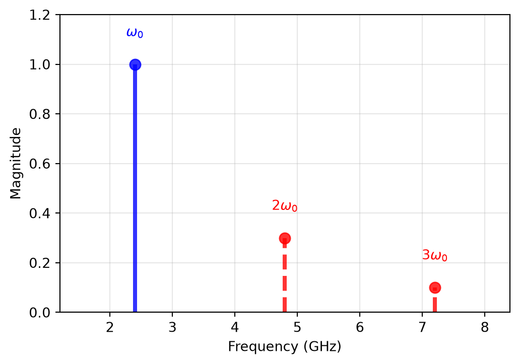
The created harmonics are illustrated in Figure 5 . Note that measuring harmonics to quantify the nonlinearity metrics like \(\alpha_2\) and \(\alpha_3\) is often not very accurate, as these harmonics are often filtered in bandwidth-limited systems.
Single-Tone Linearity
\[
A_\mathrm{1dB}^2 = \frac{1 - 10^{-1/20}}{\frac{3}{4} \left| \alpha_3 / \alpha_1 \right|} \approx 0.145 \cdot \left| \frac{\alpha_1}{\alpha_3} \right|,
\tag{9}\]
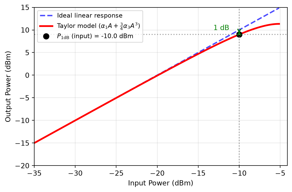
How can we quantify the nonlinearity with a one-tone test? We can sweep the input signal \(x(t)\) in amplitude, and observe the output \(y(t)\) . If the observed gain drops by 1 dB from the small-signal value, we note the input power and call this point the 1 dB compression point (\(P_\mathrm{1dB}\) ). We should always add whether this 1-dB compression point is input- or output-referred to avoid ambiguity. The diagram in Figure 6 shows this test, evaluated directly from Equation 8 with the voltage gain \(\alpha_1 = 10\) (i.e., a small-signal power gain of 20 dB) and \(\alpha_3 = -145\,\mathrm{V^{-2}}\) , referred to a 50 Ω system.
Setting the compressed gain of Equation 8 to \(10^{-1/20}\) of its small-signal value \(\alpha_1\) gives the input amplitude at the 1-dB compression point,
which for the values above lands at \(P_\mathrm{1dB} = -10\,\text{dBm}\) (input-referred). Note that the truncated third-order model is only meaningful up to its turnover point at \(A^2 = \alpha_1 / (2.25 |\alpha_3|)\) , which is a mere 4.9 dB above \(P_\mathrm{1dB}\) ; beyond that, the higher-order terms of Equation 6 (or a saturating model, see below) are required.
Single-Tone Linearity
Single-tone 1-dB compression point test, evaluated directly from the Taylor model \(y = \alpha_1 x + \alpha_3 x^3\) . The curve is only drawn up to the point where the truncated third-order model turns over and stops being physically meaningful.
Single-Tone Linearity
Compressive vs. Expansive Behavior
Note that for compressive behavior, \(\alpha_3\) and \(\alpha_1\) have different signs, while for expansive behavior, they have the same sign.
Single-Tone Linearity
\[
A_\mathrm{out} = A_\mathrm{sat} \tanh \left( u + c \cdot u^3 \right)
\]
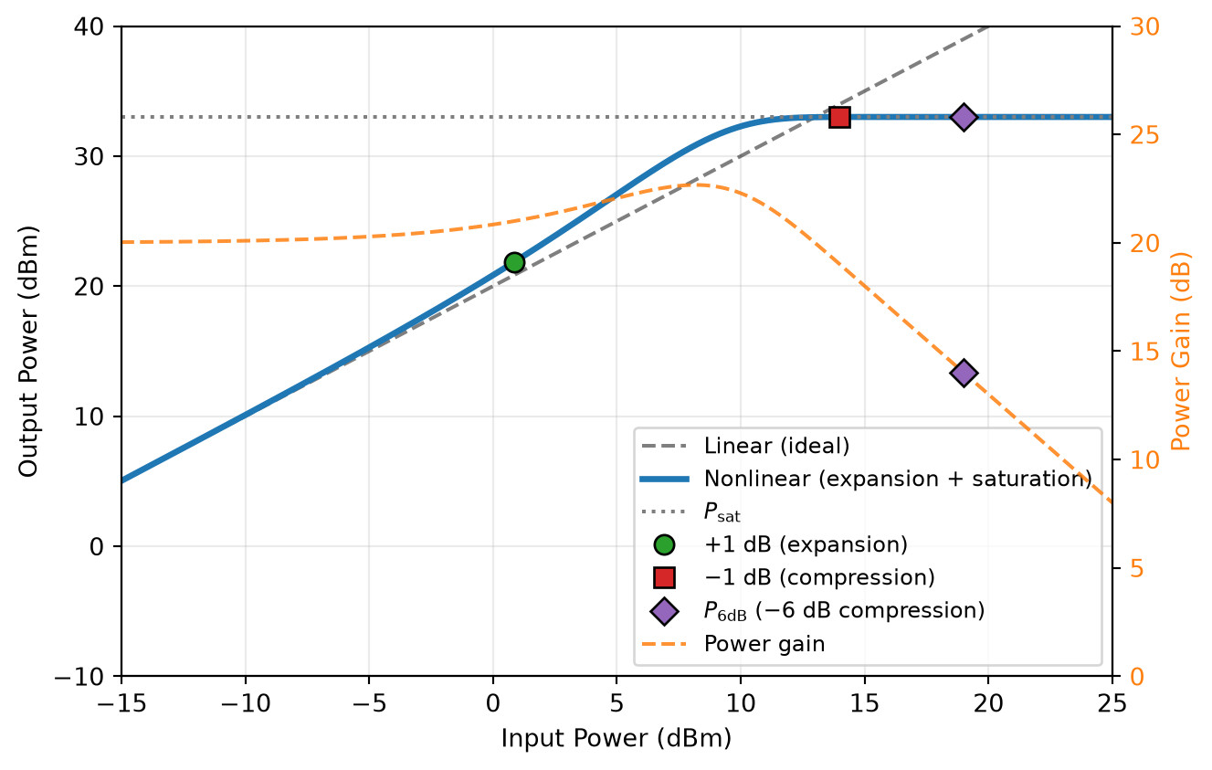
The following plot (Figure 7 ) in addition shows an expansive behavior. In contrast to the truncated Taylor-series model above, a closed-form saturating model is used here so that the output power correctly converges to the saturation power \(P_\mathrm{sat}\) for large input levels. Such saturating amplitude models are widely used to describe power-amplifier nonlinearity (Saleh 1981 ) . The model uses the amplitude characteristic
with the normalised amplitude \(u = \sqrt{G_0 P_\mathrm{in} / P_\mathrm{sat}}\) and an expansion coefficient \(c > 1/3\) . At small input powers the gain equals the small-signal gain \(G_0\) ; at intermediate powers the gain expands above \(G_0\) (because the cubic term in the argument of \(\tanh(\cdot)\) adds extra gain before the saturation takes effect); and at large input powers the output saturates at \(P_\mathrm{sat}\) while the gain drops steeply. This (partly) expansive behavior can be used to linearize the gain of a circuit block over a wider input power range, which is often desirable in RF power amplifiers (see Section 8.2 ).
Single-Tone Linearity
Output power and power gain vs. input power showing expansion, compression, and saturation towards \(P_\mathrm{sat}\) . The closed-form model uses \(P_\mathrm{out} = P_\mathrm{sat} \tanh^2 \left( u + c \cdot u^3 \right)\) with \(u = \sqrt{G_0 P_\mathrm{in} / P_\mathrm{sat}}\) . For (power) amplifiers the saturating power is often ill-defined, so instead of \(P_\mathrm{sat}\) a compression point like P6dB is used.
Multi-Tone Linearity
\[
x(t) = A_1 \cos(\omega_1 t) + A_2 \cos(\omega_2 t)
\]
\[
y(t) = y'(t) + y''(t) + y'''(t)
\tag{10}\]
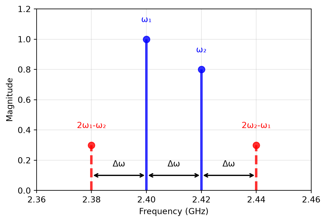
We now extend our investigations and apply two sinusoids with different frequencies \(\omega_1\) and \(\omega_2\) and different amplitudes \(A_1\) and \(A_2\) and see which signals we get at the output of the nonlinear block. The two-tone test and resulting third-order intermodulation products (IM3) are illustrated in Figure 8 .
We apply the above stimulus to our nonlinear model described by Equation 6 and again, after some trigonometric manipulations, arrive at:
As many different frequency components are created by this simple two-tone test (and nonlinearity only up to 3rd order), we split the result into different equations and look at the result separately.
Multi-Tone Linearity
To keep the following equations readable, we list only the components that are new compared to the single-tone case. The two-tone stimulus of course also produces the plain harmonics of each tone individually (at \(2 \omega_1\) , \(2 \omega_2\) , \(3 \omega_1\) , \(3 \omega_2\) ), with exactly the coefficients we already derived in Equation 7 . They are omitted below, not missing.
Multi-Tone Linearity
\[
\begin{split}
y'(t) &= \left( \underbrace{\alpha_1 A_1 + \frac{3}{4} \alpha_3 A_1^3}_\text{compression/expansion} + \underbrace{\frac{3}{2} \alpha_3 A_1 A_2^2}_\text{cross-modulation/desens} \right) \cos(\omega_1 t) \\
&+ \left( \underbrace{\alpha_1 A_2 + \frac{3}{4} \alpha_3 A_2^3}_\text{compression/expansion} + \underbrace{\frac{3}{2} \alpha_3 A_2 A_1^2}_\text{cross-modulation/desens} \right) \cos(\omega_2 t)
\end{split}
\tag{11}\]
First, we start with the fundamental tones:
As shown in Equation 11 , interesting things happen:
We (again) have the gain compression/expansion effect as already discussed in Section 2.2.1 .
In addition, we have cross-modulation , i.e., the squared envelope of one tone (e.g., \(A_2(t)\) of the tone at \(\omega_2\) ) impacts the envelope of the other tone at \(\omega_1\) . This can lead to unwanted signal distortion, even if there is a large frequency separation between \(\omega_1\) and \(\omega_2\) !
Further, since the sign of \(\alpha_3\) is usually opposite to \(\alpha_1\) , this can also lead to desensitization (“desens”). If, for example, \(A_2 \gg A_1\) , then there would be no compression due to the tone \(\omega_1\) itself, however, the large tone at \(\omega_2\) will lead to gain compression of the tone at \(\omega_1\) ; this effect is called desens.
Multi-Tone Linearity
Gain compression/expansion (as in Section 2.2.1 )
Cross-modulation : the envelope of one tone modulates the other, even for a large frequency separationDesensitization (“desens”): a large tone at \(\omega_2\) compresses a weak tone at \(\omega_1\)
Multi-Tone Linearity
\[
\begin{split}
y''(t) &= \frac{1}{2} \alpha_2 A_1^2 + \frac{1}{2} \alpha_2 A_2^2 \\
&+ \alpha_2 A_1 A_2 \cos[ (\omega_1 - \omega_2) t] \\
&+ \alpha_2 A_1 A_2 \cos[ (\omega_1 + \omega_2) t]
\end{split}
\tag{12}\]
We now look at the next class of generated tones:
As we can see in Equation 12 , new tones are created (besides the low frequency components we already know from the single-tone test) at the sum and difference of \(\omega_1\) and \(\omega_2\) . These new frequency components are called “intermodulation products of second order ” (IM2). These tones are created by the even-order nonlinearity (\(\alpha_2\) ). These IM2 products are far away from the wanted tones, so they are often not very problematic in amplifiers (but there can be exceptions!). However, they can be very problematic in frequency conversion blocks like mixers. We will come back to this point when discussing zero-IF receivers.
We now investigate the next couple of tones:
Multi-Tone Linearity
\[
\begin{split}
y'''(t) &= \frac{3}{4} \alpha_3 A_1^2 A_2 \cos[(2 \omega_1 + \omega_2) t] \\
&+ \frac{3}{4} \alpha_3 A_1^2 A_2 \cos[(2 \omega_1 - \omega_2) t] \\
&+ \frac{3}{4} \alpha_3 A_1 A_2^2 \cos[(2 \omega_2 + \omega_1) t] \\
&+ \frac{3}{4} \alpha_3 A_1 A_2^2 \cos[(2 \omega_2 - \omega_1) t]
\end{split}
\tag{13}\]
The tones shown in Equation 13 are called “intermodulation products of third order ” (IM3), and are caused by the odd nonlinearities (like \(\alpha_3\) ). While the IM3 tones located at \(2 \omega_1 + \omega_2\) and \(\omega_1 + 2 \omega_2\) are similar to the sum IM2 tone and far away from \(\omega_1\) and \(\omega_2\) , the other two tones are concerning.
Expressing \(\Delta \omega = \omega_2 - \omega_1\) (and assuming \(\omega_1 < \omega_2\) ), the construction rule \(2 \omega_1 - \omega_2 = \omega_1 - \Delta \omega\) and \(2 \omega_2 - \omega_1 = \omega_2 + \Delta \omega\) results in new tones right beside \(\omega_1\) and \(\omega_2\) , with a frequency separation only defined by \(\Delta \omega\) . This situation is illustrated in Figure 8 .
Multi-Tone Linearity
This close proximity of the IM3 tones can also be utilized to characterize nonlinear performance. Using gain compression or harmonic generation (H3), it can be very difficult to extract nonlinearity of third order (\(\alpha_3\) ). However, using a two-tone test, the IM3 tones can be readily measured, even if the measured signal path shows a bandpass characteristic ! As RF systems frequently employ bandpass filters to suppress out-of-band signals, this is a very important property of the two-tone test.
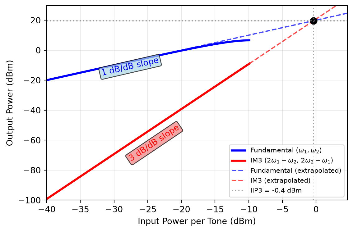
The resulting test is called a two-tone test yielding the third-order intercept point (IP3). This test is widely used in RF design to characterize the linearity of amplifiers, mixers, and complete transceiver systems. The power relationship between fundamental tones and IM3 products as a function of input power is shown in Figure 9 .
Two-tone IM3 test evaluated from the same Taylor model as Figure 6 , showing fundamental and IM3 output power vs. input power per tone, and the extrapolated IIP3/OIP3 intercept. Equal input power per tone is assumed.
Multi-Tone Linearity
\[
A_\mathrm{IIP3}^2 = \frac{4}{3} \left| \frac{\alpha_1}{\alpha_3} \right|.
\tag{14}\]
\[
\text{IIP3} = P_\mathrm{in} + \frac{P_\mathrm{in} - P_\mathrm{IM3}}{2}
\tag{15}\]
Note that, as shown in Figure 9 , the IM3 products rise with a slope of 3 dB/dB, i.e., if the input power is increased by 1 dB, the IM3 products increase by 3 dB. The fundamental tones rise with a slope of 1 dB/dB (as long as we are in the linear region). The IP3 point is defined as the intersection of the extrapolated linear lines of fundamental and IM3 products. Equating the extrapolated fundamental \(\alpha_1 A\) with the extrapolated IM3 amplitude \(\frac{3}{4} |\alpha_3| A^3\) from Equation 13 gives
As both lines have different slopes, this intersection point is usually far outside the actual operating range of the circuit block under test! Figure 9 uses the same \(\alpha_1\) and \(\alpha_3\) as Figure 6 , so both figures describe the same device: the resulting IIP3 of \(-0.4\) dBm indeed sits 9.6 dB above the \(P_\mathrm{1dB}\) of \(-10\) dBm, which is precisely the rule of thumb stated in Equation 16 below.
When calculating the IIP3 (input-referred IP3), we can use the following formula, assuming equal input power per tone. It is important to always check the slope of the IM3 products to ensure that we are indeed in the third-order region! If the input power per tone is \(P_\mathrm{in}\) (in dBm) and the input-referred power of one IM3 tone is \(P_\mathrm{IM3}\) (in dBm), then the input-referred IP3 is given by
Further, for mildly nonlinear systems (i.e., \(\alpha_3\) is dominant), the IIP3 can be approximated from the 1-dB compression point as (Razavi 2011 )
Multi-Tone Linearity
\[
\text{IIP3}|_\mathrm{dBm} \approx P_\mathrm{1dB}|_\mathrm{dBm} + 9.6\,\text{dB}.
\tag{16}\]
\[
\frac{1}{\text{IIP3}_\text{total}} \approx \frac{1}{\text{IIP3}_1} + \frac{G_1}{\text{IIP3}_2} + \frac{G_1 G_2}{\text{IIP3}_3}
\tag{17}\]
If we have multiple blocks which are cascaded, and we know the gain and IIP3 of each block, we can calculate the overall IIP3 of the cascade with the following approximation. An exact calculation is very involved, as the nonlinearities of the first block (and the resulting tones) will be processed by the second block, creating even more tones; this process escalates very quickly. However, for practical purposes, the following approximation is often sufficient:
Here \(G_1\) is the linear gain of the first block, and \(\text{IIP3}_1\) , \(\text{IIP3}_2\) are the input-referred IP3 of the first and second block, respectively. Note that all powers have to be in linear units when using Equation 17 . An even more simplified version of Equation 17 can be used with all quantities given in dBm and dB, respectively:
Multi-Tone Linearity
\[
\text{IIP3}_\text{total} \approx \min \{ \text{IIP3}_1, \text{IIP3}_2 - G_1, \text{IIP3}_3 - G_1 - G_2 \}
\tag{18}\]
A typical RF system cascade with multiple blocks and their individual IIP3 contributions is shown in Figure 10 .
Multi-Tone Linearity
Figure 10: Block cascade for IIP3 calculation showing multiple stages with gains and individual IIP3 values.
Multi-Tone Linearity
Note 4: Simple IIP3 Cascade Calculation
LNA (IIP3 = -10 dBm, gain 20 dB) followed by a mixer (IIP3 = 5 dBm, gain 10 dB). What is the overall IIP3?
Using Equation 18 we can quickly estimate:
\[
\text{IIP3}_\text{total} \approx \min \{ -10\,\text{dBm}, 5\,\text{dBm} - 20\,\text{dB} = -15\,\text{dBm} \} = -15\,\text{dBm}
\]
The second block limits the IIP3, as the LNA amplifies blockers by 20 dB before they reach the mixer.
Let’s calculate the overall IIP3 of two cascaded blocks. The first block is a low-noise amplifier with an IIP3 of -10 dBm and a gain of 20 dB. The second block is a mixer that has a gain of 10 dB and an IIP3 of 5 dBm. What is the value of the overall IIP3?
We see that the overall IIP3 is limited by the linearity of the second block, as the first block amplifies all signals (including blockers) by 20 dB before they reach the second block.
Noise
\[
\begin{split}
P_\mathrm{thermal} \big|_\mathrm{W} &= \text{PSD} \big|_\mathrm{W/Hz} \cdot B\\
&= 4 \times 10^{-21}\,\text{W/Hz} \cdot 1\,\text{MHz} = 4 \times 10^{-15}\,\text{W}
\end{split}
\]
Just as nonlinearity is a limiting factor for large signals, noise is the limiting factor for small signals. Noise is present in all electronic circuits and systems, and it is impossible to avoid it. However, we can try to minimize its impact on system performance.
Noise is usually characterized by its power spectral density (PSD) in units of Watts per Hertz (W/Hz). For example, thermal noise at room temperature has a one-sided PSD of approximately \(k T = 4 \times 10^{-21}\,\text{W/Hz}\) , or \(-174\,\text{dBm/Hz}\) (using Boltzmann’s constant \(k = 1.38 \times 10^{-23}\,\text{J/K}\) ). This means that if we have a bandwidth of 1 MHz, the total thermal noise power would be
or
Noise
\[
\begin{split}
P_\mathrm{thermal} \big|_\mathrm{dBm} &= \text{PSD} \big|_\mathrm{dBm/Hz} + 10 \log_{10} \left( \frac{B}{1\,\text{Hz}} \right)\\
&= -174\,\text{dBm/Hz} + 10 \log_{10} \left( \frac{1\,\text{MHz}}{1\,\text{Hz}} \right) = -114\,\text{dBm}.
\end{split}
\]
The PSD of noise can be flat vs. frequency (which is called “white noise”), or can decrease with frequency (e.g., “flicker noise” or “1/f noise”). Further, noise can be generated by resistors (thermal noise), semiconductors (shot noise, generation-recombination noise), etc. A detailed discussion of noise sources can be found in (Gray et al. 2009 ; Razavi 2017 ) .
Types of Noise Generation
Resistors generate thermal noise (also called Johnson-Nyquist noise ), which is white noise with a one-sided PSD of \(4 k T R\) (in V\(^2\) /Hz) when looking at the voltage across the resistor, or \(4 k T / R\) (in A\(^2\) /Hz) when looking at the current through the resistor. This noise is generated by the random thermal motion of charge carriers in the resistor.
Types of Noise Generation
\(4 k T R\) is the Rayleigh-Jeans approximation; including quantum effects (Planck) gives (Pozar 2011 )
\[
\text{PSD} = \frac{4 R h f}{e^{{h f}/{k T}} - 1}
\]
Rayleigh-Jeans holds for \(f \ll k T / h \approx 6\,\text{THz}\) at 290 K. Integrating over all frequencies bounds the noise:
\[
\overline{v_\mathrm{n}^2} = \int_0^\infty \frac{4 R h f}{e^{{h f}/{k T}} - 1} df = \frac{2 (\pi k T)^2}{3 h} \cdot R
\]
That is approx. 13 mVrms for 1 k\(\Omega\) at room temperature (not measurable in any bandwidth-limited setup).
Note that the simple approximation given above is only valid for reasonably low frequencies and typical temperatures, and is known as the Rayleigh-Jeans approximation. The full expression of Planck’s blackbody radiation, accounting for quantum effects, is given by (Pozar 2011 )
where \(h\) is the Planck constant (\(h = 6.626 \times 10^{-34}\,\text{J s}\) ) and \(f\) is the frequency. The Rayleigh-Jeans approximation is valid for \(f \ll k T / h\) , which is approximately 6 THz at room temperature (290 K).
We can integrate the above single-sided PSD over the full frequency range and show that the rms noise voltage of a resistor \(R\) is bounded to
which equates to approximately 13 mVrms noise voltage for a 1 k\(\Omega\) resistor at room temperature (which is impossible to measure in practice, as there will be some form of bandwidth limitation in any real measurement setup).
Types of Noise Generation
Equivalence of Shot and Thermal Noise
Note that it has been shown in (Sarpeshkar et al. 1993 ) that thermal noise and shot noise are actually equivalent, as both are generated by the random, thermally agitated motion of charge carriers!
MOSFETs generate several types of noise, the most important ones being the thermal noise of the channel and flicker noise.
The thermal noise of the channel can be modeled as a current noise source between the drain and source terminals with a one-sided PSD of \(\overline{I_\mathrm{n}^2} = 4 k T \gamma g_{d0}\) (in A\(^2\) /Hz), where \(\gamma\) is a process-dependent parameter (usually between 2/3 and 2). The parameter \(g_{d0}\) is the drain-source conductance of the MOSFET at \(V_\mathrm{DS} = 0\) (i.e., in deep triode); in saturation it is commonly approximated by \(g_{d0} \approx g_\mathrm{m}\) .
In saturation, it is often useful to express the thermal noise as a voltage noise source at the gate with a PSD of \(\overline{V_\mathrm{n}^2} = 4 k T \gamma / g_\mathrm{m}\) (in V\(^2\) /Hz). We can see that we can lower this noise of the MOSFET by increasing the transconductance \(g_\mathrm{m}\) , which can be achieved by increasing the bias current.
In addition, at high frequencies, the MOSFET also has induced gate-current noise, which is correlated with the channel thermal noise. A detailed discussion of this noise source can be found in (Razavi 2017 ) .
Flicker noise is usually modeled as a voltage noise source at the gate with a PSD of \(K_f / (C'_\mathrm{ox}W L f)\) (in V\(^2\) /Hz), where \(K_f\) is a process-dependent parameter, \(C'_\mathrm{ox}\) is the oxide capacitance per unit area, \(L\) and \(W\) are the length and width of the MOSFET, and \(f\) is the frequency. Note that we can lower the flicker noise by increasing the area of the MOSFET (\(W \cdot L\) ), however, this increases the parasitic capacitances associated with the MOSFET, and this is often prohibitive for RF operation!
In bipolar junction transistors (BJTs) , the most important noise source is the shot noise due to the diffusion current in the base-emitter junction. It can be modeled as a current noise source between the collector and emitter terminals with a one-sided PSD of \(2 q I_\mathrm{C}\) (in A\(^2\) /Hz), where \(q\) is the elementary charge (\(q = 1.6 \times 10^{-19}\,\text{C}\) ) and \(I_\mathrm{C}\) is the dc collector current.
Types of Noise Generation
A Note on Circuit Noise Calculations
Replace noise PSDs by equivalent sinusoidal generators in a small bandwidth (typically 1 Hz)
\(\overline{V_\mathrm{n}^2} = \overline{v_\mathrm{n}^2} / \Delta f\) and \(\overline{I_\mathrm{n}^2} = \overline{i_\mathrm{n}^2} / \Delta f\) are their mean-square values, so ordinary sinusoidal circuit analysis appliesIndependent sources: add the mean-square contributions at the output
Ideal capacitors and inductors do not generate noise; however, real-world capacitors and inductors have parasitic resistances which generate thermal noise.
In RF systems, additional noise sources can be present. One noteworthy example is the cosmic microwave background atmospheric noise , which is generated by natural phenomena like lightning or in the ionosphere.
When doing circuit noise calculations, it is instructive to keep the following points in mind:
For circuit calculations involving noise sources, it is convenient to replace the power spectral density by equivalent sinusoidal generators in small bandwidths (typically 1 Hz).
The noise power spectral density in a small bandwidth \(\Delta f\) is given by \(\overline{V_\mathrm{n}^2} = \overline{v_\mathrm{n}^2} / \Delta f\) and \(\overline{I_\mathrm{n}^2} = \overline{i_\mathrm{n}^2} / \Delta f\) .
The quantities \(\overline{V_\mathrm{n}^2}\) and \(\overline{I_\mathrm{n}^2}\) can be considered the mean-square value of sinusoidal generators. Using these values, network noise calculations reduce to familiar sinusoidal circuit-analysis calculations using \(V_\mathrm{n}\) and \(I_\mathrm{n}\) .
Multiple independent noise sources can be calculated individually at the output, and the total noise in bandwidth \(\Delta f\) is calculated as a mean-square value by adding the individual mean-square contributions from each sinusoid.
Noise in Impedance-Matched Systems
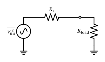
We now want to calculate the maximum noise power that can be extracted from a noisy source. We assume the following situation as shown in Figure 11 . Note that the voltage source \(\overline{V_\mathrm{n,s}^2}\) models the thermal noise of the source resistor \(R_\mathrm{s}\) resulting in a Thevenin equivalent circuit.
Noise in Impedance-Matched Systems
Figure 11: A noise-matched system with source and load impedances.
Noise in Impedance-Matched Systems
\[
P_\mathrm{n,load} = \frac{\overline{V_\mathrm{n,load}^2}}{R_\mathrm{load}} = \frac{\overline{V_\mathrm{n,s}^2}}{4 R_\mathrm{s}} = k T
\tag{19}\]
\[
\overline{V_\mathrm{n}^2} = 4 k T \Re \{ Z \}
\tag{20}\]
We know that the noise of the source resistor is given by \(\overline{V_\mathrm{n,s}^2} = 4 k T R_\mathrm{s}\) . We assume the load resistor \(R_\mathrm{load}\) as noiseless and matched to the source resistor, i.e., \(R_\mathrm{load} = R_\mathrm{s}\) for maximum power transfer . The noise power spectral density delivered to the load resistor is then given by
The calculation of Equation 19 confirms the initial statement that the maximum noise power spectral density that can be extracted from a noisy source is \(k T\) (in W/Hz). This result is independent of the actual value of the source resistance \(R_\mathrm{s}\) .
We can further generalize the thermal noise of any impedance as
as for example in the complex impedance \(Z_\mathrm{ant}\) of an antenna. Since an antenna is a reciprocal device, if we measure its radiation impedance \(Z_\mathrm{rad}\) (for example with a vector network analyzer ), we can calculate its thermal noise with Equation 20 to \(\overline{V_\mathrm{n}^2} = 4 k T \Re \{ Z_\mathrm{rad} \}\) .
Noise Figure
Note that the SNR can be improved by filtering, as filtering reduces the noise power. If the noise bandwidth is larger than the signal bandwidth, then the SNR can be improved without affecting the signal. However, this is not considered in the noise factor, as the noise factor assumes that both signal and noise pass through the same bandwidth.
Noise Figure
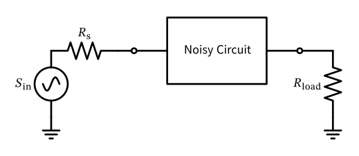
Figure 12: A noise-matched system with source and load impedances and a noisy circuit block.
Let us look at a simple model of a noisy circuit block as shown in Figure 12 . The input signal \(S_\mathrm{in}\) is accompanied by noise \(N_\mathrm{in}\) . By definition, it is assumed that the input noise power results from a matched resistor at \(T_0 = 290\,\text{K}\) , so that \(N_\mathrm{in} = k T_0\) . The circuit block has a power gain \(G\) and adds its own noise \(N_\mathrm{dut}\) to the output signal. For simplicity, we assume that the input and output of the circuit block are impedance matched to avoid reflections.
Noise Figure
\[
S_\mathrm{out} = G S_\mathrm{in}
\]
\[
N_\mathrm{out} = G N_\mathrm{in} + N_\mathrm{dut}
\]
The output signal and noise powers are then given by
The resulting noise factor can then be calculated as
Noise Figure
\[
F = \frac{{S_\mathrm{in}}/{N_\mathrm{in}}}{{S_\mathrm{out}}/{N_\mathrm{out}}} = \frac{1}{G} \frac{G N_\mathrm{in} + N_\mathrm{dut}}{N_\mathrm{in}} = 1 + \frac{N_\mathrm{dut}}{G N_\mathrm{in}},
\]
in other words, the noise factor is 1 plus the ratio of the noise added by the device under test (DUT) to the amplified input noise.
Note that a noiseless block (\(N_\mathrm{dut} = 0\) ) has a noise factor of \(F=1\) . A passive block with loss factor \(L\) (and impedance matched at input and output) has a noise factor of \(F=L\) (in linear units), as it attenuates the signal and \(N_\mathrm{out} = N_\mathrm{in} = k T\) if everything is in thermal equilibrium.
Noise Figure
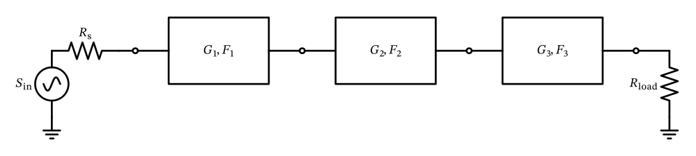
Figure 13: Block cascade for noise factor calculation showing multiple stages with gains and individual noise factors.
Noise Figure
\[
F_\mathrm{total} = 1 + (F_1 - 1) + \frac{F_2 - 1}{G_1} + \frac{F_3 - 1}{G_1 G_2}
\tag{22}\]
If we have a cascade of multiple blocks, as shown in Figure 13 , we can calculate the overall noise factor with the Friis formula (Pozar 2011 )
where \(F_i\) and \(G_i\) are the noise factor and power gain of the \(i\) -th block, respectively. Note that all gains have to be in linear units (not dB) when using Equation 22 . We can interpret Equation 22 as follows:
The overall noise factor \(F_\mathrm{total}\) is always larger than or equal to the noise factor of the first block (\(F_1\) ).
The noise factor of the first block is the most important one, as the noise factors of the following blocks are reduced by the gain of all preceding blocks. This is especially important in RF receivers, where the first block is usually a low-noise amplifier (LNA) with a very low noise figure (e.g., 1 dB or less) and a high gain (e.g., 10 dB or more). This ensures that the noise of the following blocks is negligible.
The noise factor of the last block is reduced by the gain of all preceding blocks, so it is usually not very important.
Noise Figure
\(F_\mathrm{total} \geq F_1\) The first block matters most: later noise factors are divided by the preceding gain, hence an LNA with low NF and high gain
The last block is usually negligible
Sensitivity
\[
P_\mathrm{in, min} = P_\mathrm{n} \cdot \text{SNR}_\mathrm{min} \cdot F
\tag{23}\]
\[
P_\mathrm{n} = k T B
\]
Here we also see a trade-off between noise and linearity, as shown by Equation 17 and Equation 22 . For low noise, we should try to maximize \(G_1\) , however, this will affect linearity (IIP3) in a negative way. As in many other situations in RF design, we have to find a good compromise between conflicting requirements.
In RF receivers, we often want to know the minimum input signal power that can be detected with a certain SNR. This minimum input signal power is called the sensitivity of the receiver. The sensitivity can be calculated as
where \(P_\mathrm{n}\) is the noise power at the input, \(\text{SNR}_\mathrm{min}\) is the minimum detectable SNR (i.e., the SNR required to demodulate the signal with given accuracy in terms of bit error rate or signal fidelity), and \(F\) is the noise factor of the receiver. The input noise power can be calculated as
where \(k\) is Boltzmann’s constant, \(T\) is the temperature in Kelvin, and \(B\) is the noise bandwidth of the receiver. Expressing Equation 23 in dB/dBm we get the following formula:
Sensitivity
\[
P_\mathrm{in, min}|_\mathrm{dBm} = -174\,\text{dBm/Hz} + \text{NF} + 10 \log_{10}(B/\text{Hz}) + \text{SNR}_\mathrm{min}|_\mathrm{dB}
\tag{24}\]
where -174 dBm/Hz is the thermal noise PSD at room temperature (290 K). We can see that the sensitivity reaches lower dBm values with lower noise figure, smaller bandwidth, and lower minimum detectable SNR.
Sensitivity
Note 5: Sensitivity Calculation for Wi-Fi
Let’s calculate the sensitivity of a Wi-Fi receiver operating at 5 GHz with a noise bandwidth of \(B = 80\,\text{MHz}\) , a noise figure of \(\text{NF} = 7\,\text{dB}\) , and a minimum detectable SNR of 25 dB. This high SNR means that a high-order modulation scheme (like 64-QAM) is used for high data rates.
Using Equation 24 we get: \[
P_\mathrm{in, min} = -174\,\text{dBm/Hz} + 7\,\text{dB} + 10 \log_{10} (80 \times 10^6) + 25\,\text{dB} \approx -63\,\text{dBm}
\]
This means that the minimum input signal power that can be detected by the Wi-Fi receiver is approximately -63 dBm.
Modulation
\[
s(t) = A \cos(\omega_0 t + \varphi)
\]
In order to transmit information via an EM wave, we need to modulate the wave with the information signal. Looking at a simple sinusoidal carrier wave
we see that we can change one or more of the following parameters to encode information:
Modulation
Amplitude \(A(t)\) (amplitude modulation, AM; the digital form is called amplitude-shift keying, ASK )
Frequency \(\omega_0(t)\) (frequency modulation, FM; the digital form is called frequency-shift keying, FSK )
Phase \(\varphi(t)\) (phase modulation, PM; the digital form is called phase-shift keying, PSK )
Amplitude \(A(t)\) and phase \(\varphi(t)\) (quadrature amplitude modulation, QAM )
The modulation formats FM and PM have the advantage that the carrier amplitude \(A\) is constant, which makes them more robust against nonlinear distortion.
QAM is widely used in modern communication systems, as it allows to transmit more bits per symbol by combining amplitude and phase modulation. The QAM type with four different symbols is called QPSK. Higher-order modulation formats like 16-QAM, for example, use 16 different symbols, which can encode four bits per symbol (as \(2^4 = 16\) ). Even higher-order QAM formats like 64-QAM (6 bits per symbol), 256-QAM (8 bits per symbol), 1024-QAM (10 bits per symbol), or 4096-QAM (12 bits per symbol) are also used in modern systems like Wi-Fi or LTE/5G NR.
Modulation
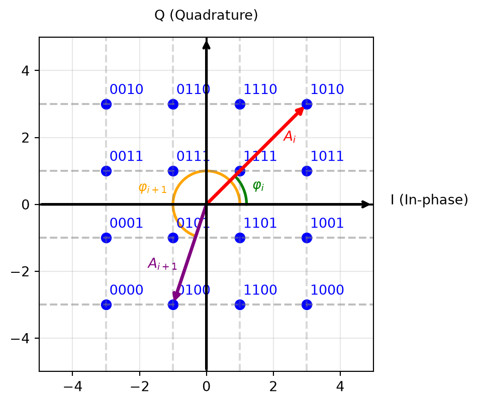
Shown in Figure 14 is the constellation diagram of a 16-QAM modulation format. The constellation points are arranged in a square grid, with each point representing a unique combination of amplitude and phase. The distance between the constellation points determines the robustness against noise and interference; larger distances result in better performance, but also require more power. The mapping of bits to constellation points is called “bit mapping” or “symbol mapping”. The example in Figure 14 uses a Gray code mapping, which minimizes the number of bit errors in case of a symbol error (assuming that a symbol will be wrongly decoded as one of its neighbors).
The constellation diagram can be imagined as a complex plane, where the x-axis represents the in-phase component (I) and the y-axis represents the quadrature component (Q) of the modulated signal. During transmission of a specific symbol, the RF carrier is modulated to the corresponding amplitude \(A_i\) and phase \(\varphi_i\) , resulting in a specific point in the constellation diagram. In Figure 14 , the amplitude and phase information for two consecutive symbols, \(A_i\) /\(\varphi_i\) and \(A_{i+1}\) /\(\varphi_{i+1}\) , is shown. If we have a bitrate with a bit duration of \(T_\mathrm{b}\) , the symbol duration for 16-QAM (4 bits per symbol) is \(T_\mathrm{s} = 4 T_\mathrm{b}\) . During the first \(T_\mathrm{s}\) , the carrier is modulated to \(A_i\) /\(\varphi_i\) (encoding 4 bits), and during the next \(T_\mathrm{s}\) , it is modulated to \(A_{i+1}\) /\(\varphi_{i+1}\) (encoding the next 4 bits).
Table 3 shows the SNR requirements for different modulation formats to achieve a bit error rate (BER) of \(10^{-5}\) in an additive white Gaussian noise (AWGN) channel (Sklar and Harris 2020 ) . As we can see, higher-order modulation formats require higher SNR to achieve the same BER. Note that for the SNR values of this table no error correction coding (ECC) is assumed; with error correction coding the required SNR can be significantly reduced!
The two columns of Table 3 are related by the number of bits per symbol,
Modulation
\[
\frac{E_\mathrm{s}}{N_0} \bigg|_\mathrm{dB} = \frac{E_\mathrm{b}}{N_0} \bigg|_\mathrm{dB} + 10 \log_{10}(k),
\tag{25}\]
and it is worth being careful about which of the two a given data sheet or standard quotes — they differ by more than 10 dB for the high-order formats. Note also that BPSK and QPSK require the same \(E_\mathrm{b}/N_0\) : QPSK transmits two bits per symbol on two orthogonal carriers, so it doubles the spectral efficiency of BPSK entirely for free in terms of energy per bit. From 16-QAM upwards, each step to the next-higher square QAM order costs roughly 6 dB in \(E_\mathrm{s}/N_0\) , because the number of constellation points quadruples while the constellation is squeezed into the same average power.
Pulse Shaping and Spectral Efficiency
Pulse Shaping and Spectral Efficiency
\[
S(f) = T_\mathrm{b} \cdot \text{sinc}^2(fT_\mathrm{b}) = T_\mathrm{b} \cdot \left[ \frac{\sin(\pi f T_\mathrm{b})}{\pi f T_\mathrm{b}} \right]^2
\tag{26}\]
When we modulate symbols onto a carrier, the question is how we transition from one symbol \(A_i\) /\(\varphi_i\) to the next symbol \(A_{i+1}\) /\(\varphi_{i+1}\) . If we change the amplitude and/or phase of the carrier instantaneously (like with a step function), we will have a very wide spectrum, which is not desirable.
Therefore, we often apply pulse shaping to the symbols, which means that we smooth the transitions between symbols. This is usually done by convolving the symbol sequence with a pulse shaping filter, which has a certain impulse response. The choice of the pulse shaping filter affects the bandwidth of the transmitted signal and its spectral efficiency.
A simple pulse shape is the rectangular pulse , which has a sinc-shaped spectrum. However, the function \(\text{sinc}(x) = \sin(\pi x)/(\pi x)\) has side lobes that extend to infinity and roll off only slowly, which can cause interference with adjacent channels.
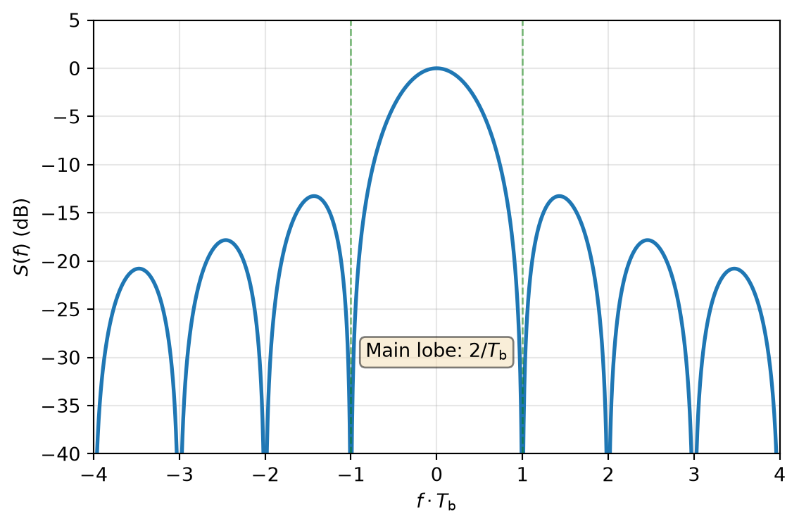
For reference, the two-sided power spectral density \(S(f)\) of a random binary sequence with equal probability of \(-1\) and \(1\) , using rectangular pulses with a duration of \(T_\mathrm{b}\) , is given by (Sklar and Harris 2020 )
and visualized in Figure 15 .
Pulse Shaping and Spectral Efficiency
Power spectral density of a rectangular pulse with duration \(T_\mathrm{b}\) . The main lobe has a bandwidth of \(2/T_\mathrm{b}\) , but the side lobes extend to infinity with slow roll-off, causing potential interference with adjacent channels.
Pulse Shaping and Spectral Efficiency
\[
p(t) = \frac{\sin(\pi t / T_\mathrm{s})}{\pi t / T_\mathrm{s}} \cdot \frac{\cos(\alpha \pi t / T_\mathrm{s})}{1 - (2 \alpha t / T_\mathrm{s})^2}
\]
As can be seen in Figure 15 , the main lobe of the sinc function has a bandwidth of \(2/T_\mathrm{b}\) , but the side lobes are quite pronounced with a slow roll-off. This means that a significant amount of power is present outside the main lobe, which can cause interference with adjacent channels.
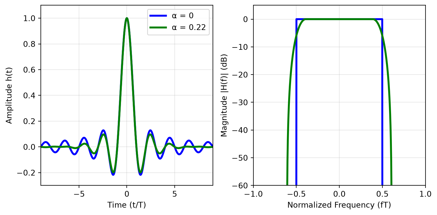
To avoid this, we can use pulse shapes that have better spectral properties, such as the raised cosine pulse or the root-raised cosine pulse. The raised-cosine pulse (see the raised-cosine filter , which satisfies the Nyquist ISI criterion) has a roll-off factor \(\alpha\) that determines the excess bandwidth beyond the Nyquist bandwidth. The root-raised cosine (RRC) pulse is used in practical systems (with half the pulse filter implemented at the TX, and half at the RX), as it can be implemented with a matched filter at the receiver.
The raised-cosine pulse \(p(t)\) (with a spectrum shaped like a raised cosine) is defined by (\(T_\mathrm{s}\) being the symbol duration, which for an \(n\) -bit-per-symbol modulation is \(T_\mathrm{s} = n \, T_\mathrm{b}\) ):
Setting \(\alpha = 0\) results in a sinc pulse in the time domain (with a perfect bandwidth containment in the frequency domain), while \(\alpha = 1\) results in a pulse with double the Nyquist bandwidth. The pulse shape for \(\alpha = 0\) and \(\alpha = 0.22\) (used in 3G) is shown in Figure 16 .
Pulse Shaping and Spectral Efficiency
Pulse Shaping and Spectral Efficiency
\[
p(t) = \frac{\sqrt{\pi}}{\alpha} e^{-(\pi t / \alpha)^2} \quad \text{with} \quad \alpha = \frac{\sqrt{\ln 2}}{\sqrt{2}} \cdot \frac{T_\mathrm{b}}{B T_\mathrm{b}}
\]
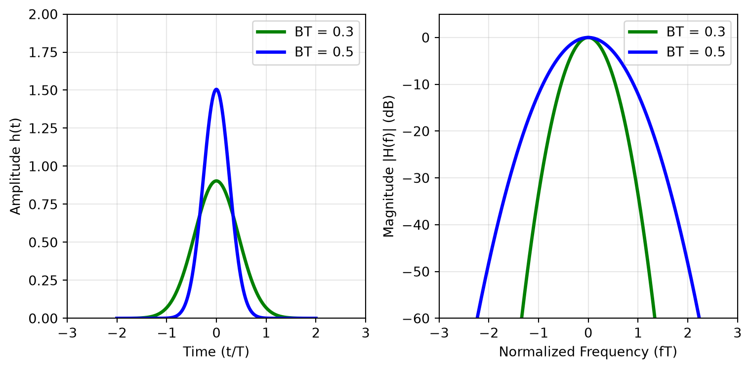
Another often-used pulse shape is the Gaussian pulse , which is used in Gaussian minimum-shift keying (GMSK , used in 2G) modulation, or in Gaussian frequency-shift keying (GFSK , used in Bluetooth). The Gaussian pulse has a smooth shape and a narrow spectrum. The Gaussian pulse is defined by:
where \(B T_\mathrm{b}\) controls the width of the pulse. The spectrum of the Gaussian pulse is also Gaussian-shaped, which helps to minimize inter-symbol interference (ISI).
The Gaussian pulse for \(B T_\mathrm{b} = 0.5\) (as used in Bluetooth) is shown in Figure 17 .
Pulse Shaping and Spectral Efficiency
Orthogonal Frequency-Division Multiplexing (OFDM)
For all the shown pulse shapes (rectangular, raised-cosine, and Gaussian), the trade-off between time- and frequency-domain containment is clearly visible. This is also captured in “Küpfmüller’s uncertainty principle ” (Küpfmüller 1949 ) , which states that the product of the time duration and the bandwidth of a pulse is lower-bounded by a constant. In other words, if we want to have a pulse that is very short in time, it will have a wide bandwidth, and vice versa.
Orthogonal Frequency-Division Multiplexing (OFDM)
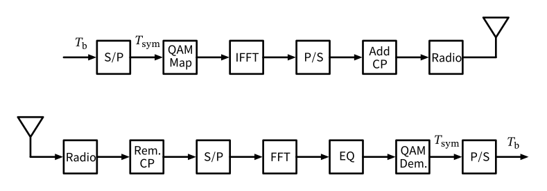
Figure 18: OFDM transmission system block diagram showing transmitter (top) and receiver (bottom) processing chains.
As we have seen in the previous section, if we make the symbol rate high, we need to use short pulses with a wide bandwidth. The problem with a wide bandwidth in wireless communication is multi-path propagation (Molisch 2022 ) , which causes frequency-selective fading. This means that some frequency parts of the channel are attenuated more than others, which can cause errors in the received signal. Equalizing such a frequency-selective channel can be very complex, especially if the channel changes rapidly (as in mobile communication).
We now face a dilemma: How can we achieve high data rates (which require high symbol rates and thus wide bandwidth) while avoiding frequency-selective fading? The key idea, implemented in orthogonal frequency-division multiplexing (OFDM) (Molisch 2022 ) , is to split the wideband channel into multiple narrow sub-channels (subcarriers), each with a low symbol rate. This way, each subcarrier experiences essentially flat fading, which is much easier to equalize.
The key question is now how to implement this idea efficiently , as we now have to apply modulation to hundreds or thousands of individual subcarriers. The solution is to use the inverse fast Fourier transform (IFFT) at the transmitter to generate the time-domain OFDM signal from the frequency-domain symbols, and the fast Fourier transform (FFT) at the receiver to recover the frequency-domain symbols from the time-domain OFDM signal. This process is illustrated in Figure 18 .
Orthogonal Frequency-Division Multiplexing (OFDM)
LTE downlink parameters:
Subcarrier spacing 15 kHz, CP 4.7 µs (5.2 µs for the first symbol)
1200 subcarriers (20 MHz), QPSK to 256-QAM
From the subcarrier spacing we can calculate the symbol duration as \(T_\mathrm{sym} = 1 / \Delta f = 1 / 15\,\text{kHz} \approx 66.7\,\mu\text{s}\) .
We can calculate the raw bitrate for a 20 MHz LTE channel using 256-QAM modulation as
\[
\text{Bitrate} = N_\mathrm{sc} \cdot N_\mathrm{bps} \cdot \frac{1}{T_\mathrm{sym} + T_\mathrm{CP}} = 1200 \cdot 8 \cdot \frac{1}{66.7\,\mu\text{s} + 4.7\,\mu\text{s}} \approx 134\,\text{Mbps}
\]
After overhead approx. 100 Mbps; carrier aggregation and MIMO multiply this to gigabit rates.
The OFDM transmitter takes a block of \(N\) symbols (e.g., 64-QAM symbols) and maps them onto \(N\) subcarriers. If the serial symbol stream has a symbol duration of \(T_\mathrm{s}\) , then distributing \(N\) of these symbols over \(N\) parallel subcarriers stretches the duration seen by each individual subcarrier to \(T_\mathrm{sym} = N \cdot T_\mathrm{s}\) . This is precisely the point of OFDM: the per-subcarrier symbol becomes long compared to the delay spread of the channel, so each subcarrier sees essentially flat fading. The IFFT then generates the time-domain OFDM signal, which is transmitted over the wireless channel. Before transmission, the cyclic prefix (CP) is added to each OFDM symbol.
At the receiver, the CP is first removed, and then the FFT recovers the frequency-domain symbols, which can then be equalized (fairly simply by multiplying each subcarrier with a complex factor to correct amplitude and phase) and demodulated.
A key property of OFDM is that the subcarriers are orthogonal to each other, which means that they do not interfere with each other. This is achieved by choosing the subcarrier spacing \(\Delta f\) such that it is equal to the symbol rate \(1/T_\mathrm{sym}\) , i.e., \(\Delta f = 1/T_\mathrm{sym}\) . This way, the integral of the product of two different subcarriers over one symbol period is zero, which means that they are orthogonal.
To further improve the robustness against multi-path propagation, a CP is added to each OFDM symbol. The CP is a copy of the last part of the OFDM symbol, which is added to the beginning of the symbol. This way, if there are delayed copies of the OFDM symbol due to multi-path propagation, they will still fall within the CP and will not cause inter-symbol interference (ISI). The length of the CP should be longer than the maximum delay spread of the channel.
In LTE OFDM is used for the downlink (base station to user equipment) with the following parameters:
Subcarrier spacing: 15 kHz
CP length: 5.2 µs (first symbol) resp. 4.7 µs (following symbols), and 16.67 µs as extended CP for scenarios with large delay spreads
Number of subcarriers: 1200 (for 20 MHz bandwidth)
Modulation: QPSK, 16-QAM, 64-QAM, 256-QAM
With the overhead for control channels and error correction coding a user data rate of approximately 100 Mbps can be achieved in a 20 MHz LTE channel. This data rate can be scaled up in two independent ways: carrier aggregation combines several such 20 MHz channels into one logical link, while MIMO transmits multiple spatial layers within the same 20 MHz channel using several antennas. The two multiply, which is how modern devices reach gigabit rates.
Multiple Access Techniques
Modulation and Coding Schemes
All of the above techniques can be combined to create more efficient and flexible communication systems. For example, OFDMA can be used in conjunction with SDMA to allow multiple users to share the same frequency resources while also taking advantage of spatial diversity. Also, TDMA can be combined with FDMA to create a hybrid multiple access scheme (which has been used in 2G).
Modulation and Coding Schemes
Some operating systems and wireless drivers show the MCS (and other parameters of the Wi-Fi link) during use. A typical output might be:
MCS: 7
RSSI: -53 dBm
Interference: -92 dBm
Bandwidth: 160 MHz
MCS 7 is 64-QAM with coding rate 5/6; with 160 MHz, 2x MIMO and 0.8 µs GI up to 1441 Mbps.
In modern wireless communication systems several parameters can be adapted on the fly to the current channel conditions to optimize the data rate and reliability. These parameters include the modulation format (e.g., QPSK, 16-QAM, 64-QAM, etc.) and the error correction coding scheme (e.g., convolutional codes, turbo codes, LDPC codes, etc.). The combination of modulation format and coding scheme is called the modulation and coding scheme (MCS) . The MCS determines the number of bits per symbol and the level of error correction, which in turn affects the data rate and reliability of the communication link, as well sets the minimum required SNR.
Since there are many different MCS options available, and the receiver needs to be informed by the transmitter which MCS is used (whenever there is a change of MCS), a standardized set of MCS options is defined in most wireless communication standards. For example, the MCS options for Wi-Fi can be seen in this table , while the MCS calculation for 5G NR can be found here .
Looking up MCS 7 in the Wi-Fi MCS table linked above shows that this corresponds to 64-QAM with a coding rate of 5/6. With a bandwidth of 160 MHz, 2x MIMO and a guard interval (GI) of 0.8 µs, the maximum data rate is a whopping 1441 Mbps.