Oscillators
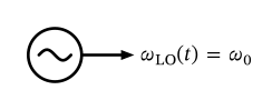
Figure 59: Oscillator symbol.
For the generation of the LO frequency to be used in a mixer for frequency conversion, oscillators are used. Ideally, oscillators produce a stable, noise-free sinusoidal signal, independent of environmental conditions like temperature or supply voltage variations. The circuit symbol of an oscillator is shown in Figure 59 .
Oscillators
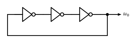
Figure 60: Three-stage single-ended ring oscillator.
The question is how to construct an oscillator. In summary, we need to build something that oscillates, i.e., produces a sustained periodic signal with frequency \(\omega_0\) . One way to achieve this is to construct a feedback loop where \(|H(s = j \omega_0)| = 1\) and \(\angle H(s = j \omega_0) = n \cdot 2 \pi\) ; these conditions are called the “Barkhausen criterion ” (here, \(H(s)\) is the loop gain around the feedback loop). A ring oscillator is one example of such a feedback oscillator. For the 3-stage single-ended ring oscillator shown in Figure 60 , each inverter contributes \(\pi\) (180°) of dc inversion plus a frequency-dependent lag caused by its output pole. At the oscillation frequency \(\omega_0\) this extra lag must be \(\pi / 3\) (60°) per stage, so that each inverter contributes \(4 \pi / 3\) (240°) in total and the three inverters together provide \(4 \pi\) , i.e., \(n \cdot 2 \pi\) with \(n = 2\) . With a single-pole model per stage this happens at \(\omega_0 = \sqrt{3}\, \omega_\mathrm{p}\) , where \(\omega_\mathrm{p}\) is the pole frequency of one inverter stage. The gain condition is fulfilled by the gain of the inverters, which must be larger than unity to compensate for losses in the loop. By using an odd number of inverters, a stable locking point at dc is avoided.
Oscillators
\[
Q = 2 \pi \frac{\text{Average energy stored}}{\text{Energy loss per cycle}} = \frac{\omega_0}{\Delta \omega} = \frac{\omega_0}{2} \sqrt{ \left( \frac{d A}{d \omega} \right)^2 + \left( \frac{d \varphi}{d \omega} \right)^2 }
\tag{55}\]
Note that the output frequency of the ring oscillator shown above is ill-controlled, as it only depends on the delay (i.e., phase shift) of the inverters, which are usually dependent on process, voltage, and temperature (PVT) variations. Also, the inherent quality factor of such an oscillator is low, as exemplified by the definition of the quality factor \(Q\) as (Razavi 1996 )
with a ring oscillator having very low \(dA / d \omega\) and \(d \varphi / d \omega\) slopes (\(A(\omega)\) and \(\varphi(\omega)\) are the open loop gain and phase shift, respectively). It can be shown that \(Q \approx 1.3\) for a 3-stage ring oscillator (Razavi 1996 ) . For some applications, this might be sufficient, but in many cases, a higher \(Q\) is desired to reduce phase noise and improve frequency stability (as we will see later in this chapter).
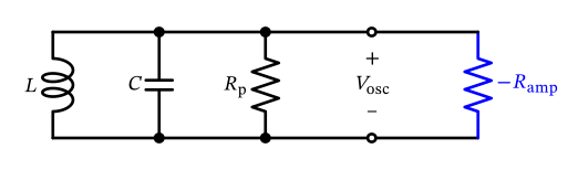
According to Equation 55 , a high \(Q\) can be achieved by using a resonator with high energy storage capability and low energy loss per cycle. We then add an amplifier in a feedback loop to compensate for the losses of the resonator. This principle is shown in Figure 61 for a parallel LC tank circuit as the resonator. Sometimes the action of the feedback loop around the amplifier is modelled as a negative resistance \(-R_\mathrm{amp}\) that compensates for the losses of the tank circuit represented by the resistor \(R_\mathrm{p}\) . The single parallel resistor \(R_\mathrm{p}\) models the losses of the inductor \(L\) and the capacitor \(C\) .
Oscillators
Figure 61: LC parallel tank with connected negative resistance forming an LC oscillator.
Oscillators
Automatic level control (ALC): measure the amplitude and adjust the gain, stable over PVTFast start-up : pre-charge \(C\) instead of waiting for noise to build up the oscillation
When \(|-R_\mathrm{amp}| = R_\mathrm{p}\) , the losses of the tank circuit are fully compensated, and we have a sustained oscillation at the resonance frequency \(\omega_0 = 1 / \sqrt{L C}\) . In practice, the amplifier gain is usually set slightly higher than required for loss compensation to start the oscillation from noise . Then, as the oscillation amplitude increases, some non-linear mechanism in the amplifier reduces the effective gain until a stable oscillation amplitude is reached. Various implementations of such LC oscillators exist, which will be discussed in the following sections.
An alternative implementation of setting the oscillation amplitude is to use an automatic level control (ALC) loop, which measures the oscillation amplitude and adjusts the amplifier gain accordingly to maintain a constant output amplitude. This approach can improve the stability of the oscillation amplitude over process, voltage, and temperature variations.
An alternative to starting the oscillation from thermal noise (which can take considerable time depending on the \(Q\) of the resonator) is to provide a known initial condition to the resonator, e.g., by pre-charging the capacitor \(C\) to a certain voltage before enabling the amplifier. This way, the oscillation can start immediately from this initial energy stored in the resonator.
Oscillators
\[
E_\mathrm{stored} = \frac{C V_\mathrm{osc,p}^2}{2}
\]
\[
E_\mathrm{loss} = \frac{V_\mathrm{osc,p}^2}{2 R_\mathrm{p}} \cdot \frac{1}{f_0}
\]
As a first hint on how to optimize an LC oscillator for low phase noise, we can try to maximize \(Q\) according to Equation 55 . The energy stored in the capacitor at peak voltage is
so to maximize this we should maximize both \(C\) and the peak oscillation voltage \(V_\mathrm{osc,p}\) . On the other hand, the energy loss per cycle is related to the power dissipated in the resistor \(R_\mathrm{p}\) by
which we can minimize by maximizing \(R_\mathrm{p}\) . In summary, to maximize \(Q\) we should use a large capacitance \(C\) , a high oscillation amplitude \(V_\mathrm{osc,p}\) , and a high tank resistance \(R_\mathrm{p}\) . Note that increasing \(C\) will reduce \(L\) for a given \(\omega_0\) . Calculating \(Q\) from these expressions yields
Oscillators
\[
Q = 2 \pi \frac{E_\mathrm{stored}}{E_\mathrm{loss}} = \omega_0 C R_\mathrm{p}
\]
\[
v_\mathrm{osc}(t) = V_\mathrm{osc,p}(t) \cdot \cos[ \omega_0(t) t + \varphi(t) ]
\]
which confirms the above observations.
Fundamentally, if we describe the output voltage of the oscillator as
we want to keep the amplitude variations small, i.e., \(V_\mathrm{osc,p}(t) = V_\mathrm{osc,p}\) , and also the frequency variations small, i.e., \(\omega_0(t) = \omega_0\) . We further want to minimize any phase fluctuations, i.e., \(\varphi(t) = \varphi_0\) .
As a side note, the definition of \(Q\) in Equation 55 can also be understood as describing how fast the energy stored in the resonator is dissipated once the excitation is removed. Per cycle, a fraction of \(2 \pi / Q\) of the stored energy is lost, so the energy decays as \(E(t) = E_0 \, e^{-\omega_0 t / Q}\) . At this rate, the stored energy would be used up after \(Q / (2 \pi)\) cycles, which is also the time after which it has fallen to \(1/e\) . For example, if \(Q = 1000\) at \(f_0 = 1\,\text{GHz}\) , this takes about 159 cycles, which is 159 ns. After \(Q = 1000\) cycles (1 µs), the energy is down to \(e^{-2 \pi} \approx 0.19\,\%\) and the amplitude to about 4 %, so the resonator has practically rung down. Both durations are sometimes called the “ring-down time” of the resonator, so it is worth stating which one is meant.
Oscillator Noise
Figure 62: LC parallel tank with oscillator in steady-state operation.
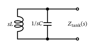
For calculating the noise of an oscillator, we assume that an LC-based oscillator as shown in Figure 61 is used. We assume that the oscillator is in steady-state operation, i.e., \(-R_\mathrm{amp} = R_\mathrm{p}\) . We can then simplify the circuit to the one shown in Figure 62 .
Oscillator Noise
\[
Z_\mathrm{tank}(s) = \frac{s L \frac{1}{s C}}{s L + \frac{1}{s C}} = \frac{s L}{1 + s^2 L C}.
\]
\[
Z_\mathrm{tank}(j \omega_0 + j \Delta \omega) =\frac{j (\omega_0 + \Delta \omega) L}{1 - (\omega_0 + \Delta \omega)^2 L C}
\]
We can calculate
At \(s = j \omega_0\) , we have \(Z_\mathrm{tank}(s) \to \infty\) , so let’s approximate around \(\omega_0\) :
For \(\Delta \omega \ll \omega_0\) , we can approximate \((\omega_0 + \Delta \omega)^2 \approx \omega_0^2 + 2 \omega_0 \Delta \omega\) and \(\omega_0 + \Delta \omega \approx \omega_0\) , which yields (using \(\omega_0^2 L C = 1\) )
Oscillator Noise
\[
Z_\mathrm{tank}(j \omega_0 + j \Delta \omega) = -\frac{j}{2 \Delta \omega C}.
\]
\[
|Z_\mathrm{tank}(j \omega_0 + j \Delta \omega)| = \frac{R_\mathrm{p}}{2 Q} \left( \frac{\omega_0}{\Delta \omega} \right)
\]
We now use the correspondence \(C = 1 / \omega_0^2 L\) and express \(L = R_\mathrm{p} / \omega_0 Q\) to get
which provides us with an expression for the magnitude of the tank impedance around resonance. We now calculate the noise power if a noise current is injected into this impedance. We use the single-sided noise current of \(R_\mathrm{p}\) (see Section 2.3.1 ), increased by a factor \(F\) contributed by the active circuit providing \(-R_\mathrm{amp}\) :
Oscillator Noise
\[
\overline{I_n^2} = \frac{4 k T F}{R_\mathrm{p}}
\]
\[
\overline{V_n^2}(\Delta \omega) = |Z_\mathrm{tank}(j \omega_0 + j \Delta \omega)|^2 \cdot \frac{4 k T F}{R_\mathrm{p}} = \frac{k T F R_\mathrm{p}}{Q^2} \left( \frac{\omega_0}{\Delta \omega} \right)^2
\]
The noise voltage across the tank at a frequency offset \(\Delta \omega\) from \(\omega_0\) is then
This absolute noise voltage is not of much interest per se. We normalize it to the oscillation amplitude \(V_\mathrm{p}\) , and only account for 1/2 of the noise, as the total noise power is split equally into amplitude noise and phase noise (Razavi 1996 ) , and we are only interested in the phase noise . This is because we assume the amplitude noise is removed by amplitude clipping in the LO chain routing the oscillator signal to the mixer. This is often a valid assumption. We introduce the symbol \(\mathcal{L}\left\{\cdot\right\}\) to denote this normalized phase noise of the oscillator:
Oscillator Noise
The phase noise \(\mathcal{L}\left\{\Delta \omega\right\}\) is expressed in the unit of dBc/Hz, i.e., in decibels of phase noise relative to the carrier power per 1 Hz of bandwidth. When expressing the phase noise of an oscillator in dBc/Hz it is important to state both the oscillation frequency \(\omega_0\) and the offset frequency \(\Delta \omega\) at which the phase noise is evaluated. For example, we could say that an oscillator has a phase noise of -137 dBc/Hz at 3 MHz offset from a carrier frequency of 2 GHz.
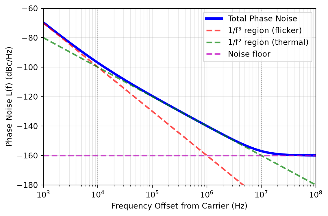
The phase noise expressed with Equation 56 describes an important region of the total oscillator phase noise where the phase noise decreases with \(1 / (\Delta \omega)^2\) , i.e., with 20 dB per decade. This region is often called the “thermal noise region” as it is dominated by thermal noise from the tank resistor and the active circuit. However, at lower offset frequencies, other noise mechanisms (like flicker noise) can dominate, leading to different slopes of the phase noise vs. offset frequency curve. At larger offset frequencies, the phase noise can flatten out due to thermal noise floor limitation of buffer amplifiers following the oscillator. A typical phase noise plot of an LC oscillator is shown in Figure 63 .
Phase noise spectrum of a typical LC oscillator showing characteristic 1/f³ and 1/f² slopes vs. frequency offset from carrier. The flicker noise corner (where the 1/f³ region transitions to the 1/f² region) is around 10 kHz, and the thermal noise floor onset is marked at 10 MHz.
Oscillator Noise
Note 7: Phase Noise and Frequency Division
Dividing the oscillator frequency by \(N\) (e.g., for IQ generation) lowers the phase noise by \(20 \log_{10}(N)\) dB, i.e., 6 dB for \(N = 2\) (Da Dalt and Sheikholeslami 2018 ) .
The divider adds its own phase noise, but the improvement usually dominates.
When using a frequency divider to generate a lower-frequency LO signal from a higher-frequency oscillator (e.g., to generate IQ phases), the phase noise of the divided signal is affected by the division ratio \(N\) (Da Dalt and Sheikholeslami 2018 ) . Specifically, the phase noise of the divided signal improves by \(20 \log_{10}(N)\) dB compared to the original oscillator phase noise. This means that if you divide the frequency by a factor of 2, the phase noise will be lowered by 6 dB!
The statement above is related to the phase noise at the output coming from the input of the divider. Of course, the frequency divider itself also contributes some additional phase noise, which can degrade the overall phase noise performance. However, in many practical cases, the improvement due to frequency division outweighs the additional noise introduced by the divider.
Jitter
The relationship between phase noise and RMS jitter can be approximated by the following equation (Da Dalt and Sheikholeslami 2018 ) : \[
\sigma_\mathrm{a} = \frac{1}{2 \pi f_0} \sqrt{2 \int_{f_1}^{f_2} \mathcal{L}\left\{f\right\} df}
\tag{58}\]
Jitter is a time-domain representation of phase noise.
It quantifies the timing variations of a periodic signal, such as the zero-crossings or rising edges of a clock signal.
Jitter is typically measured in seconds (or fractions thereof) and can be expressed as root mean square (RMS) jitter or peak-to-peak jitter.
where \(\sigma_\mathrm{a}\) is the absolute RMS jitter, \(f_0\) is the carrier frequency, and the integral is taken over the frequency offset range from \(f_1\) to \(f_2\) . This equation shows that higher phase noise levels lead to increased jitter, which can adversely affect the performance of digital communication systems by causing timing errors and signal integrity issues. Note that the phase noise \(\mathcal{L}\left\{f\right\}\) in Equation 58 must be expressed in linear scale (not dBc/Hz) when using this equation.
Reciprocal Mixing
\[
P_\mathrm{RM} = P_\mathrm{interferer} + \mathcal{L}\left\{\Delta f\right\} + 10 \log_{10}(B)
\tag{59}\]
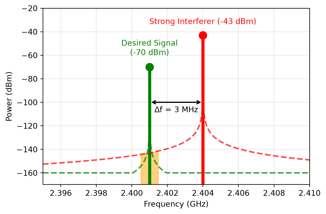
Reciprocal mixing is a phenomenon that occurs in receivers when the phase noise sidebands of the local oscillator mix with strong adjacent channel signals, resulting in in-band noise that degrades the signal-to-noise ratio of the desired signal. This effect is particularly pronounced in systems with high-order modulation schemes or closely spaced channels, where even small amounts of phase noise can lead to significant performance degradation.
To analyze reciprocal mixing, we consider a scenario where a strong interferer is present at a frequency offset \(\Delta f\) from the desired signal. The phase noise of the local oscillator at this offset frequency can be characterized by its power spectral density \(\mathcal{L}\left\{\Delta f\right\}\) . When the local oscillator mixes with the interferer, the phase noise sidebands effectively “fold” into the desired signal band, creating additional noise. This noise level can be estimated by multiplying the power of the interferer by the phase noise level at the offset frequency and considering the channel bandwidth \(B\) of the RX
where \(P_\mathrm{RM}\) is the power of the reciprocal mixing noise introduced into the desired signal band.
Reciprocal Mixing
Note 8: Reciprocal Mixing Example
Bluetooth LE RX: sensitivity -70 dBm, assumed SNR 10 dB in 1 MHz; interferer at C/I = -27 dB, 3 MHz offset. Maximum LO phase noise?
Maximum noise floor (with 3 dB margin):
\[
\begin{split}
P_\mathrm{noise,max} &= P_\mathrm{sens} - \text{SNR} - P_\mathrm{margin} \\
&= -70\,\text{dBm} - 10\,\text{dB} - 3\,\text{dB} = -83\,\text{dBm}
\end{split}
\]
\[
\begin{split}
P_\mathrm{interferer} &= P_\mathrm{sens} - \text{C/I} \\
&= -70\,\text{dBm} + 27\,\text{dB} = -43\,\text{dBm}
\end{split}
\]
Using Equation 59 , we can express the maximum allowable phase noise at 3 MHz offset at 2.4 GHz as:
\[
\begin{split}
\mathcal{L}\left\{3\,\text{MHz}\right\} &= P_\mathrm{noise,max} - P_\mathrm{interferer} - 10 \log_{10}(B/\text{Hz}) \\
&= -83\,\text{dBm} - (-43\,\text{dBm}) - 60\,\text{dB} = -100\,\text{dBc/Hz}
\end{split}
\]
Let us assume the following example from a Bluetooth LE receiver: The sensitivity target for the RX is -70 dBm, and we assume a required SNR of 10 dB in a 1 MHz bandwidth (the same assumptions as in Note 3 ; the Bluetooth LE specification itself defines the sensitivity via a bit error rate of 0.1 %, not via an SNR). An adjacent channel interferer is present at -27 dB channel to interferer ratio at an offset of 3 MHz. How much phase noise can the LO have to meet the sensitivity target?
From the sensitivity target and the SNR requirement, we can calculate the maximum allowable noise floor in the RX. We add a margin of 3 dB to account for implementation losses:
Single-Ended Oscillators
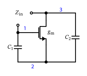
Figure 65: Circuit diagram of a single-ended negative resistance implementation.
Single-ended oscillators are commonly used in RF applications due to their simplicity and ease of integration, especially in quartz oscillators. A negative resistance is implemented using a single transistor amplifier as is shown in Figure 65 . The transistor is configured with two capacitors \(C_1\) and \(C_2\) to provide a phase-shifted feedback path.
Single-Ended Oscillators
\[
Z_\mathrm{in}(s) = -\frac{g_\mathrm{m}}{\omega^2 C_1 C_2} + \frac{C_1 + C_2}{s C_1 C_2} = -R_\mathrm{amp} + \frac{1}{s C_\mathrm{amp}}
\]
It can be shown that the differential input impedance looking into the transistor gate and drain is given by
which consists of the series combination of a negative resistance \(-R_\mathrm{amp}\) and a capacitance \(C_\mathrm{amp}\) . Note that the circuit in Figure 65 does not show a ground symbol. In fact, any of the three nodes marked with blue numbers can be used as a reference node (ground), and this results in the following well-known oscillator topologies, summarized in Table 5 .
Single-Ended Oscillators
The important insight is that the negative resistance \(-R_\mathrm{amp}\) is identical in all three cases: choosing a different reference node does not change the oscillation mechanism at all. What it does change is which node serves as the output, how the transistor is biased, and how supply and substrate noise couple into the resonator — which in practice is what decides the choice.
Single-Ended Oscillators
A Note on Oscillator Naming
Naming in Table 5 varies: grounded source is always Pierce, but grounded gate and grounded drain are both called “Colpitts” (Vittoz 2010 ) .
The Clapp oscillator is a Colpitts with a capacitor in series with the inductor (Clapp 1948 ) . A crystal has this built in: the small motional \(C_\mathrm{m}\) (Figure 66 ) makes the frequency move by only a few ppm when surrounding capacitances change (Equation 61 ).
The naming in Table 5 is not used consistently across the literature. The grounded-source case is universally called the Pierce oscillator, but both the grounded-gate and the grounded-drain variants are referred to as “Colpitts” by different authors (they differ only in which of the two capacitors provides the feedback), and some crystal-oscillator literature treats the grounded-drain circuit as just another implementation of the Pierce oscillator (Vittoz 2010 ) .
What is not a grounding variant is the Clapp oscillator : it is a Colpitts with an additional capacitor placed in series with the inductor , introduced to keep the transistor’s parasitic capacitances from pulling the frequency (Clapp 1948 ) . Interestingly, a quartz crystal oscillator gets this for free: as we will see in Figure 66 , the motional branch of a crystal is \(L_\mathrm{m}\) in series with a very small \(C_\mathrm{m}\) , so \(C_\mathrm{m}\) plays exactly the role of Clapp’s series capacitor. This is the very reason why changes of the surrounding capacitances (e.g., parasitic or transistor capacitances) move the frequency by only a few ppm (see Equation 61 ), and thus why quartz oscillators are so stable.
Single-Ended Oscillators
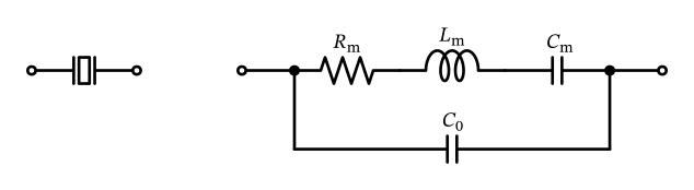
Figure 66: Quartz crystal equivalent circuit.
When we investigate the equivalent electrical circuit of a quartz crystal, we find that it has inductive behavior between its series resonance frequency and its parallel resonance frequency, which are very close together. The quartz crystal equivalent circuit is shown in Figure 66 .
Single-Ended Oscillators
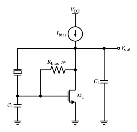
Figure 67: Circuit diagram of a single-ended Pierce crystal oscillator operating the quartz between series and parallel resonance where it acts as a large high-Q inductor.
This means we can operate the quartz crystal as a high-Q inductor in an oscillator circuit, which results in the single-ended quartz crystal oscillator shown in Figure 67 , which is a very popular choice for high-performance crystal oscillators. For an in-depth treatment of this circuit, including its start-up behavior and amplitude regulation, we recommend (Vittoz 2010 ) . Note that in a simple implementation the current-bias MOSFET can be replaced by an inverter stage biased in the linear region.
Circuit diagram of a single-ended Pierce crystal oscillator operating the quartz between series and parallel resonance where it acts as a large high-Q inductor. Note that the quartz crystal has no dc path, hence we need a high-ohmic bias resistor to connect M1 into a diode configuration.
Single-Ended Oscillators
\[
f_\mathrm{s} = \frac{1}{2 \pi \sqrt{L_\mathrm{m} C_\mathrm{m}}},
\tag{60}\]
\[
f_0 \approx f_\mathrm{s} \left[ 1 + \frac{C_\mathrm{m}}{2 (C_0 + C_\mathrm{load})} \right].
\tag{61}\]
The series combination of \(C_1\) and \(C_2\) provides the load capacitance required by the crystal to oscillate at its specified frequency. Note that the oscillation frequency is not set by \(C_\mathrm{load}\) resonating with the motional inductance \(L_\mathrm{m}\) : since the motional capacitance is tiny (\(C_\mathrm{m}\) is in the femtofarad range, while \(C_\mathrm{load}\) is in the picofarad range), the frequency is set almost entirely by the crystal itself. The oscillator runs slightly above the series resonance frequency
pulled up by the load capacitance according to (\(C_\mathrm{load}^{-1} = 1/C_1 + 1/C_2\) , and \(C_0\) being the parallel plate capacitance of the crystal)
The resulting total pulling away from \(f_\mathrm{s}\) is only in the range of some tens to hundreds of ppm, while a small change of the load capacitance moves the frequency according to the sensitivity
Single-Ended Oscillators
\[
\frac{1}{f_\mathrm{s}} \frac{\partial f_0}{\partial C_\mathrm{load}} \approx -\frac{C_\mathrm{m}}{2 (C_0 + C_\mathrm{load})^2}.
\]
For typical values of \(C_\mathrm{m} = 5\,\text{fF}\) , \(C_0 = 2\,\text{pF}\) , and \(C_\mathrm{load} = 10\,\text{pF}\) , the oscillator runs about 208 ppm above \(f_\mathrm{s}\) , but a change of \(C_\mathrm{load}\) moves it by only about 17 ppm/pF, so 0.1 pF of parasitic capacitance shifts the frequency by less than 2 ppm. Since the total pulling is nevertheless significant, crystal data sheets specify a nominal load capacitance: the designer trims \(C_1\) and \(C_2\) (often with an on-chip switched capacitor bank) to hit the specified frequency, and can use the same knob to compensate for aging and temperature drift.
Differential Oscillators
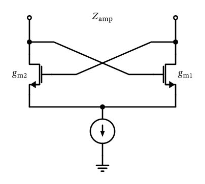
Figure 68: A cross-coupled differential pair.
After discussing single-ended oscillators in Section 6.4 , we now turn to differential oscillator topologies, which are widely used in integrated LC oscillators due to their superior common-mode noise rejection and reduced even-order harmonics. A popular way to create a differential negative resistance is to use a cross-coupled pair of transistors as shown in Figure 68 .
Differential Oscillators
\[
Z_\mathrm{in} = -\frac{2}{g_\mathrm{m}}
\]
We assume a symmetrical circuit by setting \(g_\mathrm{m1} = g_\mathrm{m2} = g_\mathrm{m}\) . By analyzing the small-signal equivalent circuit, we can derive the differential input impedance looking into the gates of the transistors:
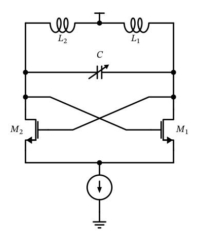
A practical implementation of a differential LC oscillator using the cross-coupled pair is shown in Figure 69 using a so-called “NMOS core”, as it is using an NMOS-based differential pair.
Differential Oscillators
Figure 69: An LC differential oscillator using an NMOS cross-coupled differential pair.
An LC differential oscillator using an NMOS cross-coupled differential pair. \(L_1\) and \(L_2\) are usually implemented as a single on-chip spiral inductor with a center tap.
Differential Oscillators
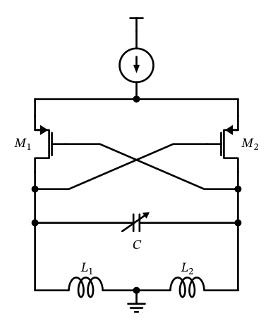
Figure 70: An LC differential oscillator using a PMOS cross-coupled differential pair.
By putting the circuit in Figure 69 on its head, we obtain a “PMOS core” oscillator, which is also widely used in integrated LC oscillators. This configuration is shown in Figure 70 .
An LC differential oscillator using a PMOS cross-coupled differential pair. \(L_1\) and \(L_2\) are usually implemented as a single on-chip spiral inductor with a center tap.
Differential Oscillators
\[
f_0 = \frac{1}{2 \pi \sqrt{L C}}
\]
In both oscillator topologies, the oscillation frequency is determined by the LC tank circuit formed by \(L = L_1 + L_2\) and \(C\) . The oscillation frequency can be approximated by
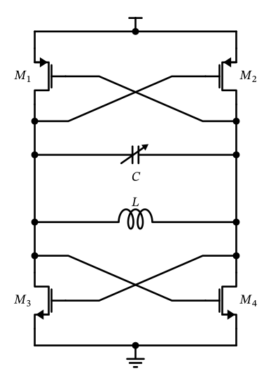
As both topologies have their inductor center tap tied to a supply rail (\(V_\mathrm{DD}\) for the NMOS core, \(V_\mathrm{SS}\) for the PMOS core), the voltage swing across the tank can go well beyond the supply voltage, which is an advantage of these topologies. However, note that the maximum voltage swing is still limited by the device breakdown voltages of \(M_1\) and \(M_2\) , which can be critical in advanced CMOS technologies with low breakdown voltages. To utilize both an NMOS and a PMOS cross-coupled pair in parallel, a so-called “complementary (or CMOS) LC oscillator” can be used, which is shown in Figure 71 . Here, the voltage swing across the tank is limited to the supply voltage, so it is inherently safe regarding device breakdown. Also, the transconductance of both NMOS and PMOS devices contributes to the negative resistance, which can reduce power consumption for a given oscillation amplitude.
Differential Oscillators
Figure 71: An LC differential oscillator using a PMOS and an NMOS cross-coupled differential pair.
Frequency Tuning of Oscillators
Note that no bias current sources are shown in Figure 71 , but can be added in practice. However, they require some voltage headroom, which lowers the maximum voltage swing across the tank, which is negative for phase noise performance according to Leeson’s equation in Equation 56 .
The inductor \(L\) used in LC tanks is often implemented as a differential spiral inductor, which can be realized on-chip using the top metal layers of the CMOS process. If higher \(Q\) is sought, then off-chip inductors must be used, which is more expensive and uses package pins to connect the inductor. Alternatively, bondwire inductors can be used, which utilize the bondwires connecting the die to the package leads as inductors. Bondwire inductors can provide high \(Q\) values and are a cost-effective solution for improving oscillator performance without requiring off-chip components. For mm-wave frequencies, transmission line stubs can be used as inductors, which can be implemented on-chip using coplanar waveguide (CPW) or microstrip structures.
Frequency Tuning of Oscillators
\[
K_\mathrm{VCO} = \frac{d f_0}{d V_\mathrm{tune}}
\]
In order to characterize the tuning sensitivity of an oscillator, the metric \(K_\mathrm{VCO}\) (voltage-controlled oscillator gain) is often used, which is defined as
with \(V_\mathrm{tune}\) being the control voltage applied to the varactor. The unit of \(K_\mathrm{VCO}\) is usually expressed in MHz/V or GHz/V. A high \(K_\mathrm{VCO}\) means that a small change in tuning voltage results in a large change in oscillation frequency, which can be beneficial for wide tuning ranges but can also make the oscillator more sensitive to noise on the tuning voltage line.
Frequency Tuning of Oscillators
Watch the Units of \(K_\mathrm{VCO}\) !
Data sheets use Hz/V; loop equations (Section 6.7 , Section 7 ) need rad/(s\(\cdot\) V):
\[
K_\mathrm{VCO} \big|_\mathrm{rad/(s \cdot V)} = 2 \pi \cdot K_\mathrm{VCO} \big|_\mathrm{Hz/V}
\]
A missing \(2 \pi\) shifts \(\omega_\mathrm{n}\) and damping by \(\sqrt{2 \pi} \approx 2.5\) , since \(\omega_\mathrm{n} \propto \sqrt{K_\mathrm{VCO}}\) ; the loop bandwidth moves even more (about \(4.7\times\) for a type-II charge-pump PLL at \(\zeta = 0.707\) ).
Data sheets and measurements state \(K_\mathrm{VCO}\) as a frequency sensitivity in MHz/V or GHz/V, as defined above. All loop equations that follow (in Section 6.7 and throughout Section 7 ) instead need the angular frequency sensitivity in rad/(s\(\cdot\) V), which is larger by a factor of \(2 \pi\) :
Forgetting this factor is one of the most common sources of error in PLL loop design: since the natural frequency scales as \(\omega_\mathrm{n} \propto \sqrt{K_\mathrm{VCO}}\) , a missing \(2 \pi\) moves \(\omega_\mathrm{n}\) by a factor of \(\sqrt{2 \pi} \approx 2.5\) , and it moves the damping factor by the same factor (in one direction or the other, depending on the loop filter used). Since both change together, the \(-3\,\text{dB}\) loop bandwidth moves by even more: for a type-II charge-pump PLL (Section 7.2 ) designed for \(\zeta = 0.707\) , a \(K_\mathrm{VCO}\) that is \(2 \pi\) larger than assumed increases the loop bandwidth by about \(4.7\times\) . In the remainder of these notes, \(K_\mathrm{VCO}\) inside loop equations is always understood to be in rad/(s\(\cdot\) V).
Frequency Tuning of Oscillators
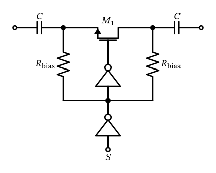
Figure 72: A switched capacitor for use in an oscillator’s switched-capacitor tuning bank.
Note that the tuning sensitivity \(K_\mathrm{VCO}\) is usually quite nonlinear over the tuning range, so it is common to specify \(K_\mathrm{VCO}\) at a certain operating point or as an average value over the tuning range.
In order to achieve a wide tuning range while maintaining a sufficiently small \(K_\mathrm{VCO}\) for phase noise reasons, a combination of coarse and fine tuning mechanisms can be used (Kral et al. 1998 ) . For example, a switched capacitor bank can provide coarse tuning steps, while a varactor can provide fine tuning within each step. It is important to ensure that the overall tuning range is free of dead zones, where the oscillator cannot be tuned to certain frequencies due to non-overlapping tuning ranges of the coarse and fine tuning elements.
While there are many ways to implement a switched capacitor for use in an oscillator tuning circuit, one popular way is shown in Figure 72 . Many such switched capacitors with different values of \(C\) (often binary weighted) can be combined to form a capacitor bank for coarse frequency tuning.
A switched capacitor for use in an oscillator’s switched-capacitor tuning bank. The bias resistors tie the drain/source nodes to ground during turn-on of \(M_1\) (for low on resistance), while they tie the drain/source nodes to VDD during turn-off of \(M_1\) to prevent accidental turn-on of the drain/source to bulk diodes of \(M_1\) .
Oscillator Modelling
Here, when the control signal \(S\) is high, the effective capacitance is \(C/2\) , with a parasitic series resistance \(R_\mathrm{on}\) due to the switch. When \(S\) is low, the effective capacitance is \(C_\mathrm{off}\) , which is the parasitic drain-source capacitance of the MOSFET switch.
Note that there exists a trade-off when designing the switched capacitor: A larger switch (with increased \(W\) ) reduces \(R_\mathrm{on}\) , but increases \(C_\mathrm{off}\) . A large \(R_\mathrm{on}\) leads to increased losses in the tank circuit, which degrades the quality factor \(Q\) and increases phase noise according to Equation 56 . On the other hand, a large \(C_\mathrm{off}\) reduces the effective tuning range of the switched capacitor, which can be detrimental if a wide tuning range is required.
In digitally-controlled oscillators (DCOs) , the tuning voltage \(V_\mathrm{tune}\) is replaced by a digital control word that selects different capacitance values from a capacitor bank. This approach allows for precise and repeatable frequency tuning, which is beneficial in applications requiring frequency synthesis or channel selection. These fine tuning steps can also be implemented according to Figure 72 ; however, the value of \(C\) must be sufficiently small.
Oscillator Modelling
\[
\omega_\mathrm{VCO}(t) = \omega_0 + K_\mathrm{VCO} \cdot V_\mathrm{tune}(t)
\]
\[
\varphi_\mathrm{VCO}(t) = \int_0^t \omega_\mathrm{VCO}(\tau) d\tau = \omega_0 t + K_\mathrm{VCO} \int_0^t V_\mathrm{tune}(\tau) d\tau.
\]
The instantaneous frequency of an oscillator can be expressed as
where \(\omega_0\) is the nominal oscillation frequency, \(K_\mathrm{VCO}\) is the tuning sensitivity, and \(V_\mathrm{tune}(t)\) is the tuning voltage applied to the varactor. Looking at the instantaneous phase \(\varphi_\mathrm{VCO}(t)\) of the oscillator, we can integrate the instantaneous frequency \(\omega_\mathrm{VCO}(t)\) to obtain
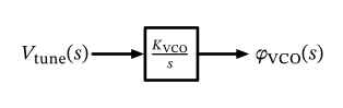
Inspecting this equation, we see that with respect to phase, an oscillator is a perfect integrator of the tuning voltage over time! For simulation purposes, we can therefore model an oscillator as an integrator block as shown in Figure 73 .
Oscillator Modelling
Figure 73: A model of a VCO as a perfect integrator for the excess phase in the \(s\) -domain.