Phase-Locked Loops
Good phase noise performance is reached with high to very high \(Q\) in the resonator (see Equation 56 ).
Oscillator tunability requires a tunable resonator, which usually results in a low-to-moderate \(Q\) , unfortunately.
Oscillators have inherent frequency stability issues due to temperature variations, device aging, and supply voltage fluctuations. However, for wireless communication systems, precise frequency control and a very stable LO (down to a few ppm of accuracy) are required.
Thinking about oscillators, we face a dilemma:
Basic PLL Architecture
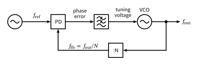
Figure 74: Block diagram of a PLL.
We solve the issues above by using a phase-locked loop (PLL) to stabilize and control the frequency of a tunable oscillator, mostly in the form of a VCO. A PLL is a feedback control system that locks the phase of the VCO output to the phase of a reference signal, typically generated by a crystal oscillator with excellent frequency stability. The block diagram of a basic PLL is shown in Figure 74 .
Block diagram of a PLL. A reference phase signal is compared to the phase of a VCO output signal in a phase detector. The phase error is low-pass filtered and used to tune the VCO frequency.
Basic PLL Architecture
\[
\Delta \varphi = 2 \pi \frac{\Delta t}{T_\mathrm{ref}}
\]
\[
V_\mathrm{error} = K_\mathrm{PD} \cdot \Delta \varphi
\]
The phase of a reference signal (often coming from a high-\(Q\) crystal oscillator) is compared to the phase of a VCO output signal in a phase detector (PD). The phase error is low-pass filtered and used to tune the VCO frequency. By continuously adjusting the VCO based on the phase difference, the PLL ensures that the VCO output remains synchronized with the reference signal, effectively combining the stability of the reference with the tunability of the VCO. When the output signal of the VCO is fed back to the phase detector through a frequency divider (with division ratio \(N\) ), the PLL can generate output frequencies that are integer multiples of the reference frequency, given by \(f_\mathrm{out} = N \cdot f_\mathrm{ref}\) .
The PD compares the phase of the reference signal with the phase of the VCO output signal. It works in the time domain and produces an output voltage proportional to the arrival time difference (phase difference) between the two input signals. This output voltage, known as the phase error signal, indicates whether the VCO is leading or lagging the reference signal in phase, expressed as
and
where \(\Delta \varphi\) is the phase difference (caused by the arrival time difference) in rad, \(K_\mathrm{PD}\) is the phase detector gain in V/rad, \(\Delta t\) is the time difference between the two signals, and \(T_\mathrm{ref}\) is the period of the reference signal.
An important consideration of the PD is its linear operating range. The PD can only provide a linear output voltage over a limited window of phase differences. For an XOR gate (or a multiplier used as a PD) this window is \(\pi\) wide: the characteristic rises linearly from \(\Delta \varphi = 0\) to \(\Delta \varphi = \pi\) and then folds back, so the loop operates around a quiescent point of \(\Delta \varphi = \pi/2\) (quadrature) with a usable range of only ±90° around it. If the phase difference exceeds this range, the PD characteristic “wraps around,” leading to ambiguity in the phase error signal. This can cause the PLL to lose lock or behave unpredictably. Therefore, the PLL design must ensure that the phase difference remains within the linear range of the PD during normal operation, which is especially troublesome if the output frequency \(f_\mathrm{out}\) is not yet close enough to its final steady-state value. Note that a simple PD can be implemented by using an XOR gate for digital signals or a mixer for analog signals.
Basic PLL Architecture
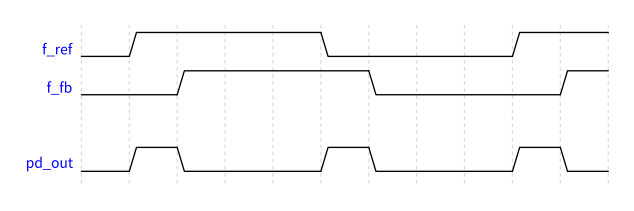
Figure 75: Input and output waveforms of an XOR-based phase detector.
Basic PLL Architecture
JK Flip-Flop Phase Detector
Instead of an XOR gate, which requires 50% duty cycle input signals, an edge-triggered JK flip-flop can be used. While the overall behavior is similar, the JK flip-flop-based PD is insensitive to duty cycle variations of the input signals, as it only evaluates the rising edges of the reference and feedback signals (Best 1999 ) .
We can see in Figure 75 that the output of the XOR PD is high when the two input signals differ and low when they are the same. The output duty cycle is proportional to the phase difference between the two input signals. Note that this PD has no notion of frequency, only phase! Still, it can be used to lock the frequency of the VCO to the reference frequency, as a constant phase difference implies equal frequencies; however, this works only if the initial frequency difference is small enough. Also, this XOR-based PD does not evaluate the edges of the input signals, only their logic states. Therefore, it is crucial that both input signals are square waves with a 50% duty cycle to ensure proper operation of the PD.
Basic PLL Architecture
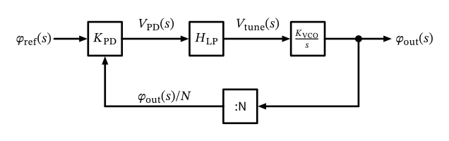
Figure 76: Laplace domain model of a PLL.
As the output signal of the PD contains high-frequency components (at least at twice the reference frequency), a low-pass filter (LPF) is used to smooth the phase error signal before it is applied to the VCO tuning input. The LPF also determines the dynamic response of the PLL, affecting its stability and transient behavior. A well-designed LPF ensures that the PLL can quickly respond to changes in the reference signal or disturbances while maintaining stability and minimizing overshoot or oscillations in the output frequency. Often, the LPF has voltage-mode inputs and outputs to connect to the PD and VCO, respectively.
Using a digital divider in the feedback path to only pass every \(N\) -th cycle of the VCO output to the PD allows the PLL to generate output frequencies that are integer multiples of the reference frequency. This is particularly useful in applications such as frequency synthesis, where a wide range of frequencies is required from a single stable reference source. By adjusting the division ratio \(N \in \mathbb{N}\) , the PLL can produce various output frequencies while maintaining phase lock with the reference signal. However, note that the frequency resolution of the output frequencies \(\Delta f_\mathrm{out}\) is limited to integer multiples of the reference frequency!
Putting everything together into an \(s\) -domain block diagram, the PLL can be modeled as shown in Figure 76 .
Laplace domain model of a PLL. Note that input and output signals are (excess) phase in rad.
Basic PLL Architecture
\[
H_\mathrm{LP}(s) = \frac{1}{1 + s T_\mathrm{LP}}.
\]
For the loop filter transfer function \(H(s)\) , we assume a simple first-order low-pass filter with a cutoff frequency of \(\omega_\mathrm{LP} = 1 / T_\mathrm{LP}\) given by
Basic PLL Architecture
Why Regulate Phase Instead of Frequency (PLL vs. FLL)?
Frequency is the derivative of phase: controlling phase controls frequency, and a steady-state phase error \(\varphi_\mathrm{err}\) still gives zero frequency error:
\[
\omega_\mathrm{out}(t) = \frac{d \varphi_\mathrm{out}(t)}{dt} = \frac{d}{dt} \left[ N \cdot \varphi_\mathrm{ref}(t) + \varphi_\mathrm{err} \right] = N \cdot \frac{d \varphi_\mathrm{ref}(t)}{dt} = N \cdot \omega_\mathrm{ref}(t).
\]
A frequency-locked loop (FLL, e.g., counter-based) usually leaves a frequency error, but helps PLL acquisition for large initial offsets.
Before we proceed, it is worth discussing why PLLs regulate the phase of the VCO output rather than its frequency directly. The reason lies in the relationship between phase and frequency: Frequency is the time derivative of phase. By controlling the phase, the PLL inherently controls the frequency as well. Additionally, even if the phase regulation has a steady-state phase error \(\varphi_\mathrm{err}\) , the frequency error in steady state is zero , as can be appreciated when inspecting
In principle, one could also design a frequency-locked loop (FLL) that compares the frequencies of the reference and VCO output signals directly (by, e.g., using counters); however, this usually results in non-zero frequency error in steady state. Nevertheless, FLLs are often used in combination with PLLs to improve acquisition time and robustness, especially in scenarios with large initial frequency offsets.
Basic PLL Architecture
\[
V_\mathrm{PD}(s) = K_\mathrm{PD} \left[ \varphi_\mathrm{ref}(s) - \frac{\varphi_\mathrm{out}(s)}{N} \right]
\]
\[
\varphi_\mathrm{out}(s) = \frac{K_\mathrm{VCO}}{s} \cdot H_\mathrm{LP}(s) \cdot V_\mathrm{PD}(s) = \frac{K_\mathrm{VCO}}{s} \cdot \frac{1}{1 + s T_\mathrm{LP}} \cdot K_\mathrm{PD} \left[ \varphi_\mathrm{ref}(s) - \frac{\varphi_\mathrm{out}(s)}{N} \right].
\]
We now derive the closed-loop transfer function of the PLL from reference phase \(\varphi_\mathrm{ref}(s)\) to output phase \(\varphi_\mathrm{out}(s)\) . First, we note that
and
Note that this equation has one integrator \(1/s\) (which we can also see in Figure 76 ). We call PLLs with one integrator in the loop a Type-I PLL . We can now rearrange to find the closed-loop transfer function \(H(s)\) as
Basic PLL Architecture
\[
H(s) = \frac{\varphi_\mathrm{out}(s)}{\varphi_\mathrm{ref}(s)} = N \cdot \frac{K_\mathrm{VCO} \cdot K_\mathrm{PD} \cdot \omega_\mathrm{LP} / N}{s^2 + s \cdot \omega_\mathrm{LP} + K_\mathrm{VCO} \cdot K_\mathrm{PD} \cdot \omega_\mathrm{LP} / N}.
\tag{62}\]
We can use all techniques known from control theory to analyze the stability and dynamic response of the PLL based on Equation 62 , however, we have to keep the following in mind:
\(H(s)\) is a small-signal model of the PLL around its locked operating point, only valid for small perturbations. Large-signal behavior, such as acquisition and lock range, is not captured by this model.A PLL is a sampled system, working at instants of \(T_\mathrm{ref}\) . \(H(s)\) is a continuous-time approximation, which is valid only if the loop bandwidth is much smaller (typically \(1/10\) ) than the reference frequency \(f_\mathrm{ref}\) . If this approximation is not valid, a discrete-time model of the PLL must be used, deriving the \(z\) -domain transfer function \(H(z)\) .
Basic PLL Architecture
\(H(s)\) is a small-signal model around lock; acquisition and lock range are not covered\(H(s)\) approximates a sampled system; valid for loop bandwidth \(\ll f_\mathrm{ref}\) (typically \(1/10\) ), otherwise use \(H(z)\)
Basic PLL Architecture
\[
H(s) = N \cdot \frac{\omega_\mathrm{n}^2}{s^2 + s \cdot 2 \zeta \omega_\mathrm{n} + \omega_\mathrm{n}^2},
\]
\[
\omega_\mathrm{n} = \sqrt{\frac{K_\mathrm{VCO} \cdot K_\mathrm{PD} \cdot \omega_\mathrm{LP}}{N}}
\tag{63}\]
If we compare the canonical form of a second-order system given by
with Equation 62 , we can identify the natural frequency \(\omega_n\) and the damping factor \(\zeta\) of the PLL as
and
Basic PLL Architecture
\[
\zeta = \frac{1}{2} \sqrt{\frac{\omega_\mathrm{LP} \cdot N}{K_\mathrm{VCO} \cdot K_\mathrm{PD}}}.
\tag{64}\]
\[
p_{1,2} = -\omega_\mathrm{n} \left( \zeta \pm \sqrt{\zeta^2 - 1} \right)
\]
This allows us to use standard control theory results to design the PLL parameters \(K_\mathrm{PD}\) , \(K_\mathrm{VCO}\) , \(\omega_\mathrm{LP}\) , and \(N\) to achieve the desired dynamic response and stability margins. Remember that \(K_\mathrm{PD}\) has to be inserted in V/rad and \(K_\mathrm{VCO}\) in rad/(s\(\cdot\) V), i.e., \(2 \pi\) times the value quoted in Hz/V (see the callout in Section 6.6 ). Note that \(\omega_\mathrm{n}\) and \(\zeta\) are not independent, as they both depend on the same set of PLL parameters! This seriously limits the design of the loop dynamics and means that we need a more complex loop filter \(H_\mathrm{LP}(s)\) to achieve more freedom in selecting \(\omega_\mathrm{n}\) and \(\zeta\) independently. Often, we want to choose \(\zeta = 1/\sqrt{2} \approx 0.707\) to achieve a maximally-flat Butterworth response with minimal overshoot.
The poles of a second-order system are given by
with \(\zeta = 1/\sqrt{2}\) resulting in complex conjugate poles at
Basic PLL Architecture
\[
p_{1,2} = -\frac{\omega_\mathrm{n}}{\sqrt{2}} \pm j \frac{\omega_\mathrm{n}}{\sqrt{2}}.
\]
To summarize: We can make a simple PLL using an XOR for a PD, use a first-order LPF, plus a feedback divider to get frequency multiplication of \(f_\mathrm{out} = N \cdot f_\mathrm{ref}\) . However, the control over the loop dynamics is very limited, and the locking procedure of the PLL is tricky, as the PD has a limited linear range of only ±90° around its quiescent point, requiring that the VCO frequency at the start of the locking procedure is already close enough to the desired output frequency. In addition, \(N\) is an integer, limiting the frequency resolution of the output frequencies to integer multiples of the reference frequency.
The question is how to improve the PLL design to overcome these limitations. We will explore advanced PLL architectures and techniques in the following section.
Charge-Pump PLL
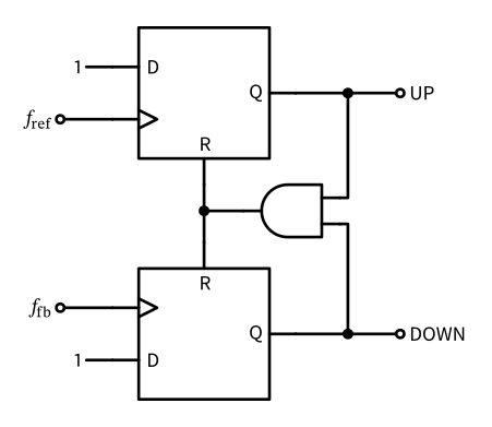
Figure 77: Implementation of a phase-frequency detector.
The fundamental limitations of the simple PLL architecture presented in Section 7.1 can be addressed by using a more sophisticated phase detector known as a phase-frequency detector (PFD) in combination with a charge pump (CP) (Gardner 1980 ) . This combination allows for better control over the loop dynamics and improved locking behavior.
In order to drive the CP, we envision a PFD with two digital outputs: an “up” signal that indicates when the VCO phase lags behind the reference phase, and a “down” signal that indicates when the VCO phase leads the reference phase (Brown 1971 ) . The PFD compares both the phase and frequency of the reference and feedback signals, providing a more robust locking mechanism. The typical implementation of a PFD is shown in Figure 77 .
Charge-Pump PLL
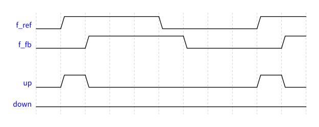
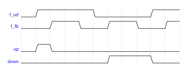
Reference leads: “UP” active, CP sources current, VCO frequency increases
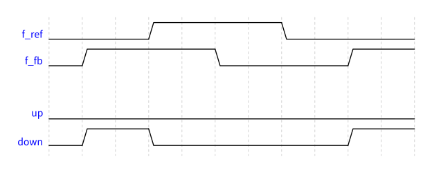
Feedback leads: “DOWN” active, CP sinks current, VCO frequency decreases
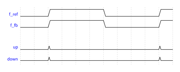
Aligned: only short pulses, loop filter capacitor holds the tuning voltage
The later edge resets both outputs: current pulse width is proportional to the phase difference
Charge-Pump PLL
Figure 78: Reference leading the VCO feedback signal, frequencies are already aligned.
Charge-Pump PLL
Figure 79: VCO feedback signal leading the reference, frequencies are already aligned.
Charge-Pump PLL
Figure 80: VCO feedback and reference signal are aligned in phase and frequency.
Charge-Pump PLL
Figure 81: VCO feedback and reference signal have different frequencies (the VCO frequency is too high).
VCO feedback and reference signal have different frequencies (the VCO frequency is too high). There will be some periods with a wrong output (as shown here in the first cycle), but on average the phase-frequency detector output will indicate that the VCO frequency must be decreased.
Charge-Pump PLL
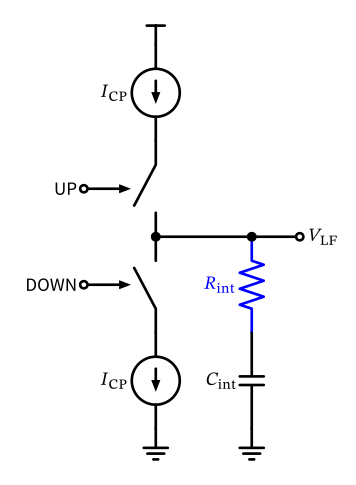
Figure 82: Charge pump consisting of two matched current sources and switches.
Let us now investigate the circuit of the CP. The UP and DOWN signals from the PFD control two current sources/sinks connected to the loop filter capacitor, as shown in Figure 82 .
Charge pump consisting of two matched current sources and switches. The resistor in series with the capacitor introduces a zero.
Charge-Pump PLL
\[
\Delta V_\mathrm{LF} = \frac{1}{C_\mathrm{int}} \int_0^{t_\mathrm{on}} I_\mathrm{CP} \cdot dt
\tag{65}\]
\[
H_\mathrm{CP}(s) = \frac{I_\mathrm{CP}}{2 \pi} \left( \frac{1}{s C_\mathrm{int}} + R_\mathrm{int} \right)
\tag{66}\]
When the UP signal is high, the CP sources a constant current \(I_\mathrm{CP}\) into the loop filter capacitor \(C_\mathrm{int}\) , increasing its voltage linearly over time according to the phase error. Conversely, when the DOWN signal is high, the CP sinks a constant current \(I_\mathrm{CP}\) from the capacitor, decreasing its voltage linearly.
Note that the top and bottom current sources must be well matched to ensure symmetric operation of the CP and should have a wide operating range. The output impedance of the CP is ideally very high so that the charge pump current does not depend on the voltage across the loop filter capacitor. Further, the switches introduce charge injection and clock feedthrough, which can cause unwanted ripples on the loop filter voltage, leading to spurious signals in the PLL output. Careful design of the switches and careful layout techniques are necessary to minimize these effects.
The voltage change on the capacitor can be expressed as
where \(t_\mathrm{on}\) is the duration for which the UP or DOWN signal is active, proportional to the phase difference between the reference and feedback signals.
Taking the Laplace transform of Equation 65 , we find the transfer function of the CP from the UP/DOWN control signals to the loop filter voltage as
where we have added a resistor \(R_\mathrm{int}\) in series with the capacitor \(C_\mathrm{int}\) to introduce a zero in the loop filter transfer function. The need for this zero will become apparent when we analyze the PLL loop dynamics next.
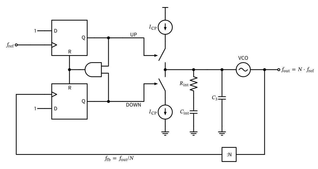
The resulting PLL using a PFD-CP combination is shown in Figure 83 .
Charge-Pump PLL
Figure 83: Diagram of a PFD-CP PLL.
Diagram of a PFD-CP PLL. Note that the capacitor \(C_3\) has been added to reduce the CP switching ripple, and its presence makes the loop filter 3rd order.
Charge-Pump PLL
\[
H(s) = \frac{\varphi_\mathrm{out}(s)}{\varphi_\mathrm{ref}(s)} = N \cdot \frac{\frac{I_\mathrm{CP} K_\mathrm{VCO}}{2 \pi C_\mathrm{int} N} (1 + s C_\mathrm{int} R_\mathrm{int})}{s^2 + s \frac{I_\mathrm{CP} K_\mathrm{VCO} R_\mathrm{int}}{2 \pi N} + \frac{I_\mathrm{CP} K_\mathrm{VCO}}{2 \pi C_\mathrm{int} N}} = N \cdot \frac{s \cdot 2 \zeta \omega_\mathrm{n} + \omega_\mathrm{n}^2}{s^2 + s \cdot 2 \zeta \omega_\mathrm{n} + \omega_\mathrm{n}^2}
\tag{67}\]
\[
\omega_\mathrm{n} = \sqrt{\frac{I_\mathrm{CP} K_\mathrm{VCO}}{2 \pi C_\mathrm{int} N}}
\tag{68}\]
Neglecting \(C_3\) for now, we can derive the closed-loop transfer function of the PLL from reference phase \(\varphi_\mathrm{ref}(s)\) to output phase \(\varphi_\mathrm{out}(s)\) as
with
and
Charge-Pump PLL
\[
\zeta = \frac{R_\mathrm{int}}{2} \sqrt{\frac{I_\mathrm{CP} K_\mathrm{VCO} C_\mathrm{int}}{2 \pi N}}.
\tag{69}\]
Looking at Equation 68 and Equation 69 , we can see that we now have one additional independent parameter (\(R_\mathrm{int}\) ) to set the natural frequency \(\omega_\mathrm{n}\) and the damping factor \(\zeta\) of the PLL independently (compare this to Equation 63 and Equation 64 ). This allows us to design the loop dynamics more flexibly to achieve the desired performance.
With Equation 69 , we can now appreciate the need for the resistor \(R_\mathrm{int}\) in series with the capacitor \(C_\mathrm{int}\) in the loop filter. Without this resistor, the damping factor \(\zeta\) would be zero, leading to an undamped system with oscillatory behavior and poor transient response. The resistor introduces a zero in the loop filter transfer function, providing the necessary damping to stabilize the PLL and improve its dynamic response.
Looking at Figure 83 and Equation 66 , we can also see that the PFD-CP introduces another integrator in the loop. This integrator, together with the integrator from the VCO, makes the PLL a Type-II PLL . A Type-II PLL achieves zero steady-state phase error not only for a step in the reference phase (which a Type-I PLL manages as well), but also for a step in the reference frequency , i.e., a ramp in the reference phase. This is the practically important case, as it means the loop settles to exactly \(\Delta \varphi = 0\) after a channel change, without the static phase offset that a Type-I PLL would exhibit. Only for a frequency ramp (a parabolic phase input) does a Type-II PLL retain a finite static phase error.
In conclusion:
The PLL regulates the phase of a VCO to match the phase of a reference signal, using feedback control. Even with a steady-state phase error, the frequency error is zero (Type-I PLL). In a Type-II PLL, both phase and frequency errors are zero in steady state.
The lowpass behavior of the loop filter determines the dynamic response and stability of the PLL.
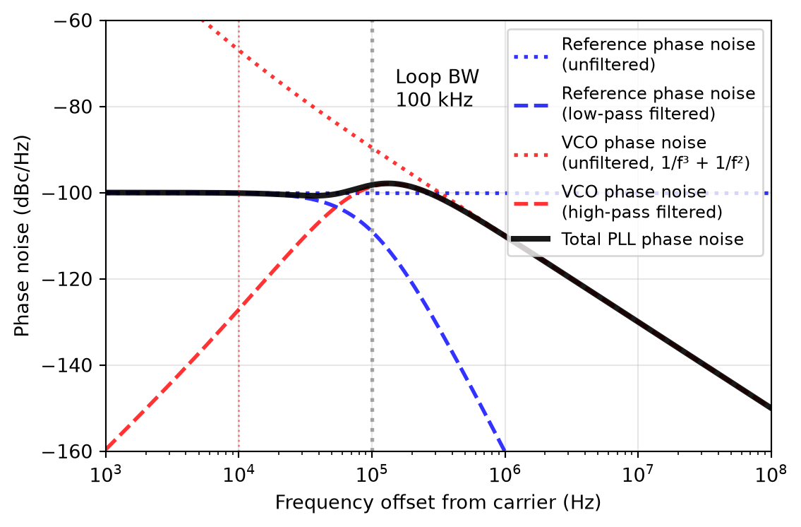
Further, the PLL transfer function from reference phase to output phase has the form of a lowpass, which passes the reference oscillator phase noise to the output inside the passband. The phase noise of the VCO is suppressed inside the loop bandwidth, as the PLL corrects for phase deviations.
Outside the PLL loop bandwidth, the VCO phase noise dominates, as the PLL cannot correct for phase deviations fast enough.
Charge-Pump PLL
The PLL locks the VCO phase to the reference; zero frequency error in steady state (Type-II: zero phase error, too)
The loop filter sets dynamics and stability
Inside the loop bandwidth: reference phase noise passes (lowpass), VCO phase noise is suppressed
Outside the loop bandwidth: VCO phase noise dominates
Charge-Pump PLL
This phase noise shaping behavior is illustrated in Figure 84 , which shows how the reference and VCO phase noise contributions combine to form the total PLL output phase noise.
PLL phase noise contributions at the PLL output showing reference phase noise (increased by 20*log(N) and low-pass shaped), VCO phase noise (high-pass shaped), and total phase noise. The loop bandwidth determines the crossover frequency between reference and VCO phase noise contributions. For effective rejection of the 1/f³ VCO phase noise, a higher-order loop filter (shown is 3rd order) is beneficial.
All-Digital PLL
Note that inside the PLL loop bandwidth the reference phase noise is multiplied by \(N^2\) in power, i.e., \(20 \log_{10}(N)\) in dB, as the PLL output frequency is \(N\) times the reference frequency. In Figure 84 , \(N = 100\) and a reference phase noise of -140 dBc/Hz is used. Large values of \(N\) can significantly increase the reference phase noise contribution at the PLL output, which is why low phase noise references are essential for high-performance PLLs.
All-Digital PLL
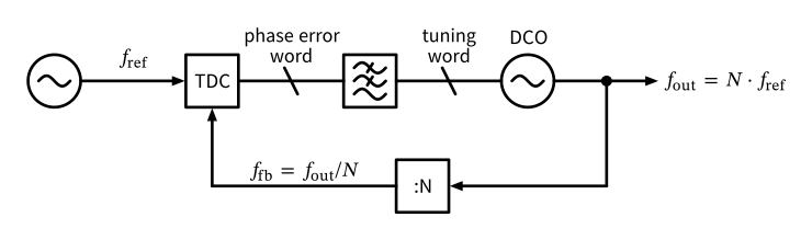
Figure 85: Block diagram of an all-digital PLL.
In the PLL implementations discussed so far, we have used analog components such as the VCO, loop filter, and charge pump. While these analog PLLs can achieve excellent performance, they also come with challenges such as component variability, temperature sensitivity, and integration complexity in modern digital processes. The question arises: Can we implement a PLL using only digital components to overcome these challenges? The answer is yes, leading to the concept of the all-digital phase-locked loop (ADPLL) (Staszewski et al. 2003 ) , whose block diagram is shown in Figure 85 .
Block diagram of an all-digital PLL. A reference phase signal is compared to the phase of a digitally-controlled oscillator (DCO) output signal in a time-to-digital converter (TDC). The phase error word is digitally low-pass filtered and used to tune the DCO frequency via a frequency control word.
Time-to-Digital Converter
Conceptually, the ADPLL in Figure 85 is similar to the analog PLL in Figure 74 , with the key difference being that all components are implemented digitally. The phase detector is replaced by a time-to-digital converter (TDC), which measures the time difference between the reference and feedback signal edges and converts it into a digital phase error word. The loop filter is implemented as a digital filter (FIR, IIR, or similar), processing the phase error word to generate a tuning word for the digitally controlled oscillator (DCO). The DCO generates the output frequency based on the tuning word, completing the feedback loop.
The advantages of the ADPLL are that it can be fully integrated in a digital nm CMOS process, benefiting from scalability, low power consumption, small chip area, and immunity to analog component variations. Additionally, the digital nature of the ADPLL allows for easy programmability and adaptability to different applications. However, the ADPLL also faces challenges such as quantization noise from the TDC and DCO, nonlinearity (DNL and INL) of TDC and DCO, as well as coupling of digital switching noise into the oscillator output signal.
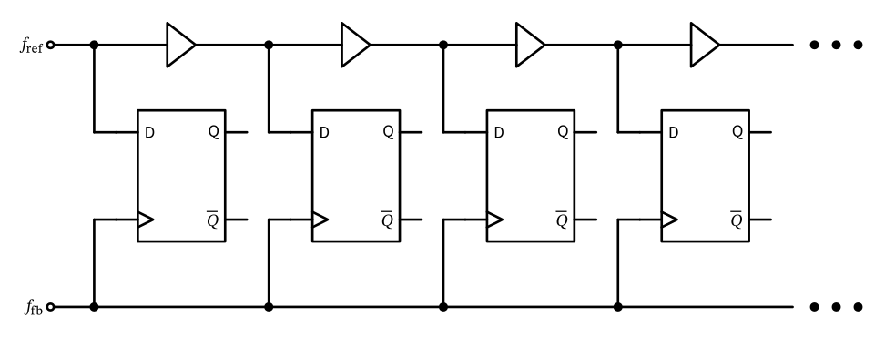
The TDC is a crucial component of the ADPLL, responsible for measuring the time difference between the reference and feedback signal edges and converting it into a digital phase error word. The TDC operates by sampling the time interval between two events (the rising edges of the reference and feedback signals) and quantizing this interval into discrete levels. TDCs can be implemented using various techniques. One popular method is using a digital delay line. An exemplary implementation is shown in Figure 86 .
Time-to-Digital Converter
Figure 86: Basic TDC implementation as a delay line with parallel capture flip-flops.
Basic TDC implementation as a delay line with parallel capture flip-flops. The TDC delay resolution is limited to two inverter delays.
Time-to-Digital Converter
\[
\mathcal{L}\left\{f\right\} = 10 \cdot \log \left[ \frac{(2 \pi)^2}{12 f_\mathrm{ref}} \cdot \left( \frac{\Delta T_\mathrm{TDC}}{T_\mathrm{DCO}} \right)^2 \right]
\]
In Figure 86 , the reference signal edge runs through a series of buffers (delay elements) connected in a delay line configuration. The feedback signal edge is used to sample the state of the delay line at the moment it arrives. The outputs of the DFFs represent the time difference between the reference and feedback signals, which can be encoded into a digital phase error word. The resolution of the TDC is determined by the delay between each stage in the delay line, with finer delays providing higher resolution. However, increasing the resolution also increases the complexity and power consumption of the TDC.
The phase noise of the TDC (at the output of the ADPLL) arising from this time measurement quantization can be modeled as
where \(\Delta T_\mathrm{TDC}\) is the time resolution of the TDC, \(T_\mathrm{DCO}\) is the period of the DCO output frequency, and \(f_\mathrm{ref}\) is the reference frequency. This equation shows that improving the TDC resolution (reducing \(\Delta T_\mathrm{TDC}\) ) and increasing the reference frequency can help reduce the phase noise contribution from the TDC.
Time-to-Digital Converter
To get an idea of the performance requirements for the TDC, we assume a DCO output frequency of 2.4 GHz (e.g., for a Bluetooth application) and a reference frequency of 40 MHz. If we aim for a TDC phase noise contribution of -100 dBc/Hz at the DCO output, we can rearrange the above equation to find the required TDC time resolution:
\[
\Delta T_\mathrm{TDC} = T_\mathrm{DCO} \cdot \sqrt{\frac{12 f_\mathrm{ref} \cdot 10^{\mathcal{L}\left\{f\right\}/10}}{(2 \pi)^2}} = \frac{1}{2.4 \times 10^9} \cdot \sqrt{\frac{12 \cdot 40 \times 10^6 \cdot 10^{-10}}{(2 \pi)^2}} \approx 15\,\text{ps}
\]
This number is challenging but achievable with modern TDC designs in nm CMOS.
Digitally Controlled Oscillator
Figure 87: Digitally controlled oscillator using a DAC.
Digitally Controlled Oscillator
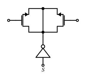
Figure 88: A switched differential varactor used for fine frequency control in a DCO.
Fractional-N PLL
It has to be noted that while an ADPLL seems conceptually simpler than an analog PLL, the design of high-performance TDCs and DCOs can be quite complex and requires careful consideration of quantization noise, linearity, and power consumption. Coupling effects between different circuit blocks can also introduce unwanted spurs and phase noise folding in the ADPLL output. Therefore, while ADPLLs offer many advantages, they also present unique design challenges that must be addressed to achieve adequate performance.
Fractional-N PLL
\[
N = N_1, N_1, N_1, N_2 \implies \text{Average } N = \frac{61 + 61 + 61 + 62}{4} = 61.25
\]
\[
N = \frac{99 \cdot 61 + 1 \cdot 62}{100} = 61.01
\]
With the PLL architectures discussed so far, the output frequency resolution is limited to integer multiples of the reference frequency, i.e., \(f_\mathrm{out} = N \cdot f_\mathrm{ref}\) with \(N \in \mathbb{N}\) . For a fine output frequency resolution, this requires a very low reference frequency. With the rule of thumb that the PLL loop bandwidth should be less than \(f_\mathrm{ref}/10\) to ensure stable operation, a low reference frequency also limits the achievable loop bandwidth, which is detrimental to phase noise performance and settling time. Further, we have learned in Section 7.2 that large values of \(N\) increase the reference phase noise contribution at the PLL output by \(20 \log_{10}(N)\) dB, making it challenging to achieve low phase noise performance with high frequency resolution.
How to break these fundamental limitations? The answer lies in the concept of the fractional-N PLL , which allows for non-integer frequency multiplication.
Assume we want to generate an output frequency of \(f_\mathrm{out} = 2.45\,\text{GHz}\) from a reference frequency of \(f_\mathrm{ref} = 40\,\text{MHz}\) . This requires a frequency multiplication factor of \(N = 61.25\) , which is not an integer. To achieve this, the fractional-N PLL employs a feedback divider that can switch between two integer division ratios, \(N_1\) and \(N_2\) , such that the average division ratio over time equals the desired fractional value (the averaging is performed by the low-pass loop filter, providing the averaged tuning voltage to the VCO / the tuning word to the DCO). In this case, we can choose \(N_1 = 61\) and \(N_2 = 62\) . By alternating between these two division ratios in a controlled manner, the PLL can effectively achieve an average division ratio of 61.25, allowing it to generate the desired output frequency of 2.45 GHz. The following sequence illustrates this concept over four reference cycles:
A simple sequence like the one above works, but would lead to significant spurs in the PLL output spectrum due to the periodic nature of the division ratio switching, especially when the fractionality is close to an integer, and thus the sequence is long. Consider the case of \(N = 61.01\) , where we would need to switch to \(N_2 = 62\) only once every 100 cycles of \(N_1 = 61\) :
This periodic switching introduces spurious tones in the PLL output spectrum at multiples of \(f_\mathrm{ref}/100\) , which can potentially pass through the loop filter and appear in the output spectrum, degrading the signal quality.
To minimize these spurs, more sophisticated techniques such as delta-sigma modulation are employed to randomize the switching sequence, spreading the quantization noise over a wider frequency range and reducing its impact on the PLL output. Additionally, the quantization noise introduced by the fractional division is pushed to higher frequencies where it can be more easily filtered out by the loop filter.
Delta-Sigma Modulator
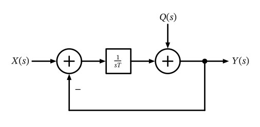
For an in-depth understanding of delta-sigma modulation, we refer to (Schreier et al. 2017 ) . Here, we briefly summarize the key concepts relevant to fractional-N PLLs. In a nutshell, a delta-sigma modulator (DSM) is a feedback system that shapes quantization noise to higher frequencies, allowing for high-resolution digital-to-analog conversion or frequency synthesis. The basic structure of a first-order DSM is shown in Figure 89 .
Delta-Sigma Modulator
Figure 89: A first-order continuous-time delta-sigma modulator.
Delta-Sigma Modulator
\[
Y(s) = X(s) \cdot \frac{1}{1 + s T} = X(s) \cdot H_\mathrm{LP}(s)
\]
\[
Y(s) = Q(s) \cdot \frac{s T}{1 + s T} = Q(s) \cdot H_\mathrm{HP}(s)
\]
In Figure 89 , the input signal \(X(s)\) is transferred to the output \(Y(s)\) with the following transfer function (we set \(Q = 0\) ):
The quantization noise \(Q(s)\) introduced by the quantizer is shaped by the feedback loop, resulting in the following output contribution:
We can see that the quantization noise is highpass filtered, pushing it to higher frequencies, where it can be more easily filtered out by a subsequent lowpass filter.
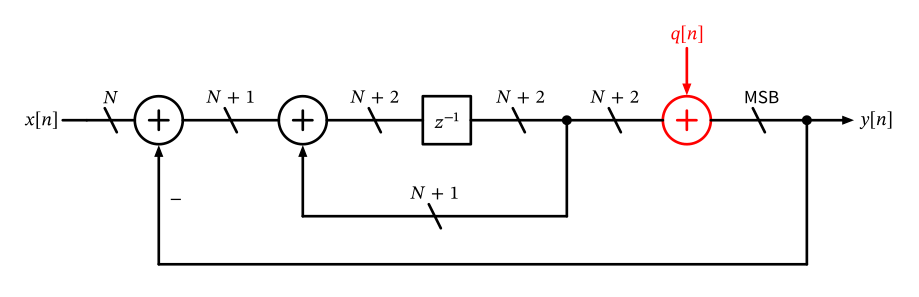
The digital implementation of a first-order DSM is straightforward and one possible form is shown in Figure 90 . At the point of truncation from \(N+2\) bits to 1 bit (the MSB) we imagine quantization noise \(q[n]\) being added to the signal.
Delta-Sigma Modulator
Figure 90: A first-order digital delta-sigma modulator.
Delta-Sigma Modulator
\[
\frac{Y(z)}{X(z)} = \text{STF}(z) = z^{-1}
\]
\[
\frac{Y(z)}{Q(z)} = \text{NTF}(z) = (1 - z^{-1}) \implies \text{NTF} = 1 - z^{-1}.
\]
Calculating the \(z\) -domain transfer functions from input \(X(z)\) to the output \(Y(z)\) (the signal transfer function, STF) and quantization noise \(Q(z)\) to \(Y(z)\) (the noise transfer function, NTF), we find
and
We see that the STF is a simple delay, while the NTF has a zero at DC, pushing the quantization noise to higher frequencies. Evaluating the frequency response of the NTF to find the frequency-shaped PSD of the quantization noise, we find
Delta-Sigma Modulator
\[
S_\mathrm{y}(f) = S_\mathrm{q}(f) |H(f)|^2 = S_\mathrm{q}(f) \cdot 2 \left| 1 - \cos(2 \pi f T_\mathrm{s}) \right| \implies H(f) = \sqrt{ 2 \left| 1 - \cos(2 \pi f T_\mathrm{s}) \right| }.
\]
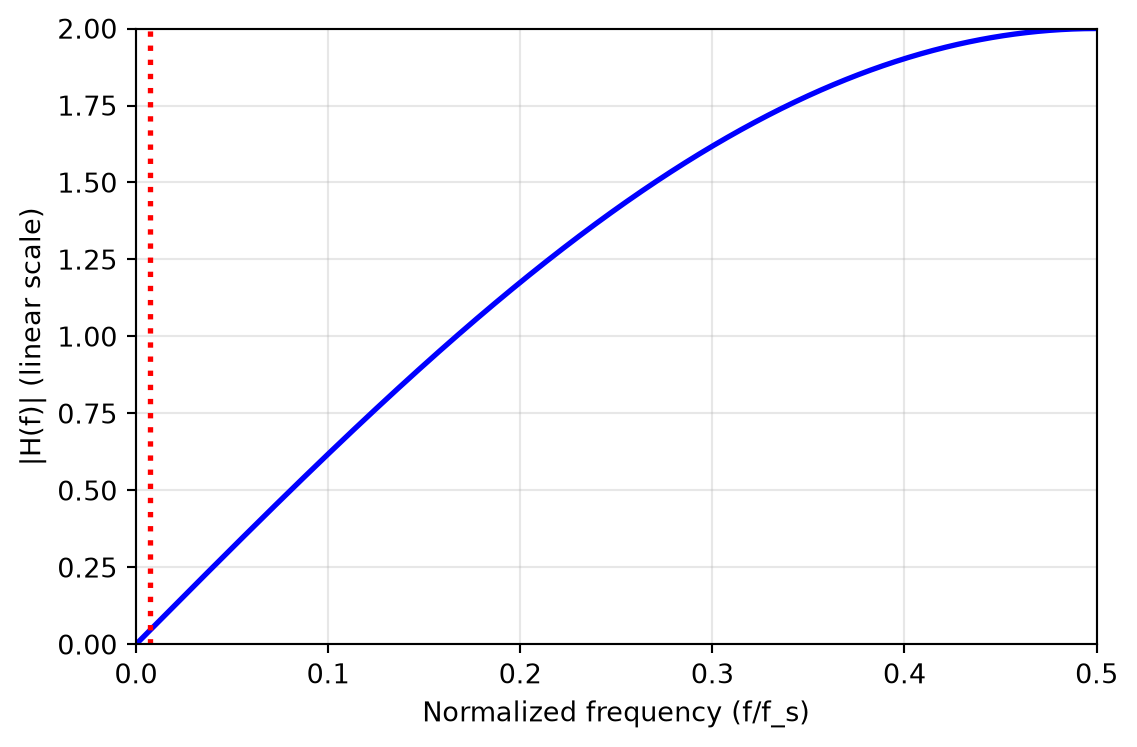
with \(T_\mathrm{s}\) being the sampling period of the DSM. The resulting \(H(f)\) is shown in Figure 91 . With the assumed PLL loop bandwidth of 100 kHz and a reference frequency of 40 MHz, we can see that the quantization noise is significantly attenuated inside the PLL loop bandwidth, minimizing its impact on the PLL output phase noise. The general trend is that higher-order DSMs and faster sampling frequencies lead to better noise shaping and lower in-band quantization noise.
Delta-Sigma Modulator
NTF H(f) of a first-order delta-sigma modulator showing the high-pass noise shaping characteristic. The quantization noise is suppressed at low frequencies and increases towards the Nyquist frequency. An exemplary loop filter bandwidth of 300 kHz for a 40 MHz reference frequency is indicated.
Delta-Sigma Modulator
If we analyze the signal properties of the number sequence generated by the first-order DSM in Figure 90 , we find that its randomization properties are not ideal, leading to spurs in the PLL output spectrum. To improve the randomization properties, higher-order DSMs are used in fractional-N PLLs, especially 2nd or 3rd order. A consequence of a higher-order DSM is that the produced sequence can take more values than just \(N\) and \(N+1\) . The range of produced values is shown in Table 6 .
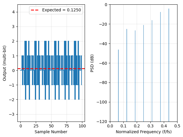
A standard 3rd-order DSM implementation has issues with stability due to the phase shift of three integrators in the feedback loop. To mitigate this, a well-known architecture called the MASH (multi-stage noise shaping) DSM is often used (Matsuya et al. 1989 ) , which consists of multiple first-order DSM stages cascaded together. An example Python implementation of a 3rd-order MASH DSM is shown in Figure 92 , showing a snippet of the time-domain output and the resulting frequency spectrum, showing the noise shaping. As can be clearly seen, even using a 3rd-order MASH, there are strong spurious signals showing up in the spectrum. The time series shows that for some static input values (like here 0.125) patterns with a short period can exist.
Delta-Sigma Modulator
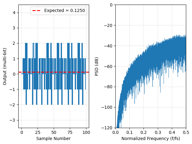
As a potential solution, we can add a very small dithering signal (i.e., adding a random signal to the input), which breaks these patterns. As shown in Figure 93 , dithering indeed causes enough randomization so that the noise shaping can be clearly seen without noticeable spurs (this is evident when comparing the time series of Figure 92 and Figure 93 ). Care has to be taken that the added random noise is small enough to not cause issues with in-band noise.
Delta-Sigma Modulator
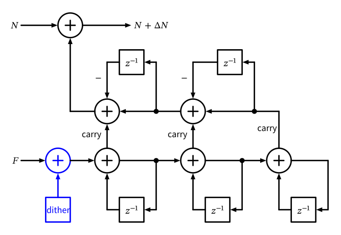
Figure 94: Block diagram of a 3rd-order MASH 1-1-1 delta-sigma modulator with three cascaded first-order stages and digital noise cancellation logic including dither injection.
A block diagram of a 3rd-order MASH 1-1-1 implementation including dither injection (shown in blue) is depicted in Figure 94 . The dither is typically implemented digitally as a pseudo-random bit sequence (PRBS) generator, often in the form of a linear-feedback shift register (LFSR).
Fractional-N PLL Implementation
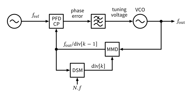
A block diagram of a fractional-N PLL using a DSM and a multi-modulus divider (MMD) is shown in Figure 95 . In order to ease the timing loop of the jittered clock coming from the MMD, the DSM is typically clocked by the MMD’s output.
Fractional-N PLL Implementation
Figure 95: Block diagram of a fractional-N PLL.
Block diagram of a fractional-N PLL. The VCO signal is divided by a sequence of integer divider values div[k] whose average value is given by \(N.f\) , where \(N\) is the integer part of the divider value and \(f\) is the fractional part of the divider.
Fractional-N PLL Implementation
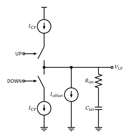
Figure 96: Charge pump with offset current for use in a fractional-N Type-II PLL.
Fractional-N PLL Implementation
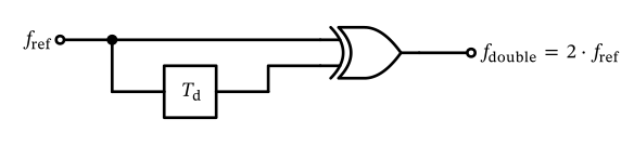
Figure 97: Implementation of reference frequency doubler.
As we have seen multiple times in the PLL discussion, using a higher \(f_\mathrm{ref}\) is beneficial for phase noise performance, loop bandwidth, and TDC resolution (in an ADPLL). However, in many applications the choice of reference frequency is constrained by other factors. One way to achieve a higher reference frequency is by using a frequency doubler . As shown in Figure 97 , a frequency doubler can be implemented using an XOR gate and a delay line. The delay line is set to a quarter of the period of the reference frequency, i.e., \(T_\mathrm{d} = T_\mathrm{ref} / 4\) . The XOR gate then produces an output frequency of \(f_\mathrm{double} = 2 \cdot f_\mathrm{ref}\) . For stable operation, this delay line must be designed to be relatively insensitive to process, voltage, and temperature (PVT) variations, or must be adjusted with a control loop.
Implementation of reference frequency doubler. Ideally, \(T_\mathrm{d}\) should be set to \(T_\mathrm{ref} / 4\) .
Fractional-N PLL Implementation
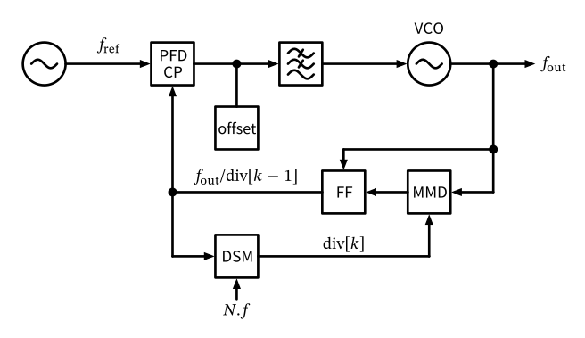
Figure 98: Block diagram of a fractional-N PLL including a retiming flip-flop to reduce the MMD-related jitter.
As a final remark, we note that the output of the MMD in Figure 95 is a jittered clock due to the changing division ratio and the multiple gates and flip-flops that make up the MMD. This jitter degrades the PLL phase noise performance. Fortunately, there is an easy fix for this issue by using a retiming flip-flop after the MMD, clocked by the oscillator output, as shown in Figure 98 .