TinyWhisper: An Open-Source Fully-Integrated Multi-Mode Short-Wave Transmitter for Amateur Radio Applications in 130-nm CMOS

This documentation is a Work in Progress.
This repository requires the IIC-OSIC-TOOLS container with tag 2026.05 or later.
1 Overview
TinyWhisper is a compact WSPR transmitter realized with the ihp-sg13g2 PDK. The 2 mm x 2 mm chip operates at a core supply voltage of 1.5 V and an I/O supply voltage of 3.3 V. The chip is packaged in a QFN-48 package with a total of 56 pins, eight of which are VSS pins connected directly to the package VSS. All documentation, presentations, design files, and future updates are publicly available here. The block diagram is shown below. A render of the final chip layout is shown below, with the digital part placed on the left side of the chip and the analog part on the right. A custom logo on the topmost metal layer, generated with the tool ArtistIC, is also shown below.
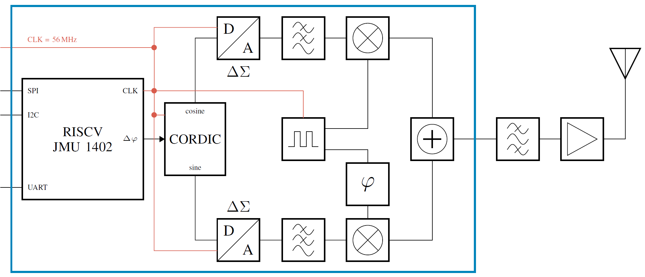
Block diagram of the TinyWhisper ASIC and external RF circuitry.
1.1 Purpose
TinyWhisper demonstrates what is possible with current open-source tools and open-source PDKs, from system design to final tapeout, from packaging to PCB design, and even to a 3D-printable enclosure. It can also be used for:
- Ham radio courses
- University courses
- Regression tests of open-source EDA tools
1.2 Weak Signal Propagation Reporter
WSPR is a popular digital transmission scheme in amateur radio, specifically designed to study propagation conditions at low transmit power. WSPR transmits a short message containing the callsign, location, and transmit power using 4-FSK modulation (tone spacing 1.46 Hz, symbol duration 0.683 s). Thanks to strong forward error correction (rate 1/2), long ranges can be achieved even at very low transmit power levels (down to 10 mW). Receivers can decode WSPR signals down to -31 dB below the noise floor of a 2500 Hz channel. Received signals are reported to a central database via the internet, enabling global analysis of signal propagation.
1.3 Digital Core
The heart of the digital core is a simple multi-cycle embedded processor based on a 32-bit RISC-V architecture running at a clock rate of 56 MHz. By using the RISC-V architecture, the CPU is directly compatible with common compilers, and programs can, for example, be written in C. The program is stored in an external SPI SRAM, from which the CPU fetches its instructions. For communication with peripherals, the chip features I2C and UART interfaces as well as digital GPIO pins that can be freely controlled.
An integrated 30-bit CORDIC algorithm generates the 4-FSK-modulated I/Q baseband signals according to the WSPR protocol. The phase increment of the CORDIC can be configured via software, allowing any frequency to be generated with a resolution of approximately 0.05 Hz. This also enables compensation for frequency errors of the external crystal oscillator. Using a second-order Delta-Sigma (DS) modulator with selectable oversampling (32, 64, 128, or 256), the parallel 30-bit data from the CORDIC is converted into a 1-bit signal that is passed directly to the analog front-end. Additionally, the digital core generates the LO frequencies listed in the table below by dividing the 56 MHz clock by two, covering the most common shortwave bands: 28 MHz, 14 MHz, 7 MHz, and 3.5 MHz.
| Band | RF Frequency | LO Frequency | IF (CORDIC) |
|---|---|---|---|
| 80m | 3.592600 MHz | 3.5 MHz | 92.600 kHz |
| 40m | 7.038600 MHz | 7 MHz | 38.600 kHz |
| 20m | 14.095600 MHz | 14 MHz | 95.600 kHz |
| 10m | 28.124600 MHz | 28 MHz | 124.600 kHz |
1.4 Analog Front-End
The analog front-end is an IQ modulator consisting of two third-order multiple-feedback (MFB) low-pass filters with a cutoff frequency of 400 kHz and a Butterworth characteristic. The amplifier core of the MFB filter is based on a Barthelemy / Manfredini (B/M) inverter-based OTA. Two passive voltage-mode mixers are driven by a 25% duty-cycle local oscillator and produce a single-ended RF output signal.
Integrated SPDT switches allow switching between the internal CORDIC/DSM signals and external analog inputs, enabling tests with an external function generator, among other uses.
Since the analog front-end is an IQ modulator, it supports not only WSPR but also other modulation schemes such as FT8, SSB, and CW. Hence, the title “TinyWhisper: An Open-Source Fully-Integrated Multi-Mode Short-Wave Transmitter for Amateur Radio Applications in 130-nm CMOS”.
1.5 Tapeout
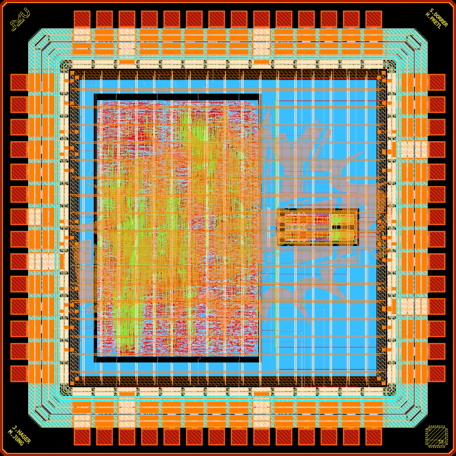
Chip render of the ihp-sg13g2 TinyWhisper ASIC (2mm x 2mm).
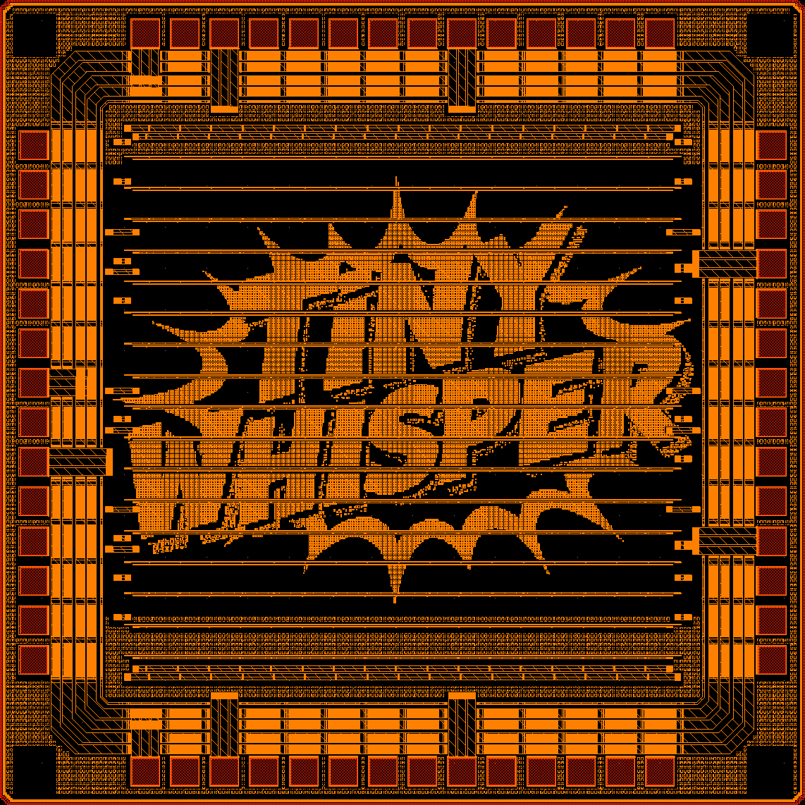
Render of the TopMetal2 TinyWhisper logo, generated with the tool ArtistIC.
1.6 Outlook
The chip is still in production and is expected to be delivered in December 2026. The ASIC is just the beginning of a broader open-hardware project. The next step is to design a PCB that includes all necessary external components: switchable bandpass filters for each RF band, an RF amplifier, a crystal oscillator as the clock source, external SRAM, voltage regulators for the various supply voltages, a display, controls, an SMA connector for the antenna, and a USB interface for configuration. The packaged chip will be soldered onto this board and then characterized.
Building on this PCB, a compact, 3D-printable enclosure is planned that accommodates the board together with a small battery and is robust enough for outdoor use during field tests and SOTA activations.
2 System Description
This TinyTapeout chip implements a transmitter for the long-range wireless protocol WSPR (weak signal propagation reporter) in the shortwave frequency range (3 MHz to 30 MHz). Transmissions last \(162 \cdot 8192 / 12000 = 110.6\,\text{s}\) and start at even UTC minutes.
2.1 MODEM
The modulation layer, which packs information into the transmit data packet, works as follows1:
- A 50-bit payload is encoded with a convolutional code with \(K=32\) and \(r=1/2\)
- Call sign of 6 characters (A-Z, 0-9, SPACE)
- Shorter call signs are padded with SPACE to result in 6 characters
- The 3rd character has to be a number, so insert SPACE in front if needed
- Locator coded with 4 characters (A-Z, 0-9) \(L_1, L_2, L_3, L_4\)
- The first pair of characters takes values from A-R and is encoded using the integers 0-17
- The second pair of characters are taken from 0-9 and are encoded as that respective number
- Finally, the locator is encoded as the integer \(M_1 = (179 - 10 \cdot L_1 - L_3) \cdot 180 + 10 \cdot L_2 + L_4\)
- Transmit power level in dBm (0 to 60)
- Call sign of 6 characters (A-Z, 0-9, SPACE)
- Number of symbols \(N_\mathrm{sym} = (50 + K - 1) \cdot r^{-1} = 162\)
- The baud rate is \(12000 / 8192 = 1.4648\,\text{baud}\)
- Synchronization is achieved with a 162-bit constant pseudo-random vector
- Interleaving is used
2.1.1 Coding of Callsign
Starting with a 6-character call sign of [A-Z], [0-9], [SPACE], represented as \(C_1, C_2, C_3, C_4, C_5, C_6\).
- Shorter call signs are padded with SPACE to result in 6 characters.
- The 3rd character (\(C_3\)) has to be a number, so insert SPACE in front if needed.
- The mapping is:
- [0]-[9] = 0-9
- [A]-[Z] = 10-35
- [SPACE] = 36
The calculation of the integer \(N\) representing the call sign is:
\[ N_1 = C_1 \] \[ N_2 = 36 \cdot N_1 + C_2 \] \[ N_3 = 10 \cdot N_2 + C_3 \] \[ N_4 = 27 \cdot N_3 + C_4 - 10 \] \[ N_5 = 27 \cdot N_4 + C_5 - 10 \] \[ N = 27 \cdot N_5 + C_6 - 10 \]
The resulting \(N\) is represented as a 28-bit integer used for transmission2.
2.1.2 Coding of Locator
Location is given as a 4-letter string of [A-Z] and [0-9], represented as \(L_1, L_2, L_3, L_4\). The mapping of the locator:
- The first two characters can be [A]-[R] so are coded as 0-17.
- The second two characters are [0]-[9] coded as 0-9.
The integer \(M_1\) is calculated as:
\[ M_1 = ( 179 - 10 \cdot L_1 - L_3) \cdot 180 + 10 \cdot L_2 + L_4 \]
This integer \(M_1\) fits into a 15-bit representation3.
2.1.3 Coding of Power Level
The transmit power level \(P\) is coded in dBm with a range of 0 to 60. The final value of \(M\) is coded as:
\[ M = 128 \cdot M_1 + P + 64 \]
\(M\) is represented as a 22-bit integer4.
2.1.4 Formation of Data Packet
The final 50-bit payload is formed by packing \(N\) (28 bit) and \(M\) (22 bit) into a 50-bit array. These 50 bits are packed into a 7-byte array D[0] to D[6] (D[0] contains the MSB of the callsign; the LSBs of D[6] are set to zero).
2.1.5 Convolutional Encoding

TBD (see http://www.g4jnt.com/Coding/WSPR_Coding_Process.pdf)
2.1.6 Interleaving
TBD (see http://www.g4jnt.com/Coding/WSPR_Coding_Process.pdf)
2.1.7 Sync Vector and Symbol Formation
The resulting 162 bits of data from convolutional coding and interleaving are then combined with a fixed 162-bit synchronization vector.
Each transmission symbol \(S_i\) (2 bit for 4-FSK) is formed by (\(b_{\mathrm{sync},i}\) is the synchronization bit and \(b_{\mathrm{data},i}\) is the data bit)
\[ S_i = b_{\mathrm{sync},i} + 2 \cdot b_{\mathrm{data},i} \]
The synchronization vector is given as a 162-bit constant5:
110000001000111000100101111000000010010100000010110011010001101000011010101010010010110001101010001000001001001110110011010001110000010100110000000110101100011000
2.1.8 Data Interface after Modulation
The final 162 two-bit symbols are packed as 4 symbols per byte (MSB first) into 41 bytes, resulting in a transmit message M[0] to M[40].
2.2 PHY
WSPR supports various RF frequencies. The frequencies supported by TinyWhisper are6:
- 3.592600 MHz (80m band)
- 7.038600 MHz (40m band)
- 14.095600 MHz (20m band)
- 28.124600 MHz (10m band)
These frequencies are the center frequencies (LO frequencies) for the WSPR transmissions. The actual RF output frequency is offset by +1500 Hz using upper-sideband (USB) modulation. For channel selection, the nominal +1500 Hz can be varied in the range of +1400 Hz to +1600 Hz.
2.2.1 Modulation
- 4-FSK with a tone spacing of 1.465 Hz (mode F1D) is used.
- The modulation tone frequencies are:
- \(f_1 = -3/2 \cdot 12000/8192 = -2.197\,\text{Hz}\) (symbol
00) - \(f_2 = -1/2 \cdot 12000/8192 = -0.732\,\text{Hz}\) (symbol
01) - \(f_3 = 1/2 \cdot 12000/8192 = 0.732\,\text{Hz}\) (symbol
10) - \(f_4 = 3/2 \cdot 12000/8192 = 2.197\,\text{Hz}\) (symbol
11)
- \(f_1 = -3/2 \cdot 12000/8192 = -2.197\,\text{Hz}\) (symbol
- The occupied bandwidth is therefore approximately 6 Hz.
- Minimum SNR for decoding is around \(-34\,\text{dB}\).
2.2.2 RF
The RF output of the TinyTapeout chip is a single-ended analog output. It can be used to connect an external power amplifier and low-pass filters to meet the required output power and spectral emissions. Further details can be found in the PCB design section.
3 Implementation
The implementation is targeting a TinyTapeout run using sky130A technology, since it allows combining digital and custom components for this WSPR transmitter.
3.1 Concept
The implementation concept is based on a few important boundary conditions listed below:
- A digital clock frequency \(f_\mathrm{clk} = 56\,\text{MHz}\) is used throughout the design. With this choice of clock frequency the identified transmit frequencies are readily supported.
- For implementation efficiency, the digital content of the architecture is maximized in contrast to the full-custom content.
3.2 Mixed-Signal Transmitter
The architectural overview is shown in Figure 2. The FSK-4 modulation is based on an analog IQ transmitter driven by a CORDIC. An IQ DAC path with a sample rate of 218.75 kSps (TBC) and a CORDIC/DSM data path width of 30 bit, followed by a 3rd-order low-pass filter, is upconverted in a passive voltage-mode mixer with 25% LO generated by a divide-by-2 circuit.

3.2.1 TX LO Generation
To support the RF frequencies listed in Section 2.2, the following LO generation concept is planned. The LO frequency is 2x the RF frequency, since the IQ phases are generated by a divide-by-2 circuit (https://iic-jku.github.io/radio-frequency-integrated-circuits/rfic.html#sec-lo-ff). If a constant 56 MHz crystal clock is used, the resulting frequency offset must be generated digitally by the CORDIC.
| RF frequency | LO frequency | LO pre-divider | CLK frequency | CORDIC frequency offset |
|---|---|---|---|---|
| 3.592600 MHz | 7 MHz | 8 | 56 MHz | 92.600 kHz |
| 7.038600 MHz | 14 MHz | 4 | 56 MHz | 38.600 kHz |
| 14.095600 MHz | 28 MHz | 2 | 56 MHz | 95.600 kHz |
| 28.124600 MHz | 56 MHz | 1 | 56 MHz | 124.600 kHz |
As the frequencies are low enough, the LO generation is implemented in HDL in src/lo_gen.v.
3.2.2 TX DACs
To simplify the analog DAC design, delta-sigma DACs (DSM) with differential single-bit outputs are used. As a compromise between implementation complexity and performance, a programmable 1st/2nd-order modulator is used, which can be implemented purely digitally in HDL with inverter-style outputs.
The output sample rate of the DS modulator is 56 MSps, and it supports OSR = 32/64/128/256. The corresponding input sample rates are given in the following table:
| OSR | Input sample rate |
|---|---|
| 32 | 1.75 MSps |
| 64 | 875 kSps (default) |
| 128 | 437.5 kSps |
| 256 | 218.75 kSps |
The general SNR formula for an \(N\)-bit, \(L\)-order DSM with OSR is7 \[ \text{SNR} = 6.02 N + 1.76 + 10 \log_{10}\biggl(\frac{2 L + 1}{\pi^{2L}}\biggr) + (2L + 1) 10 \log_{10}(\text{OSR}). \]
The SNR of a single-bit (\(N = 1\)) first-order (\(L = 1\)) DSM is given by (\(r = \log_2(\text{OSR}) = 6\) for an \(\text{OSR} = 64\)) \[ \text{SNR} = 6.02 + 9.03 r - 3.41 = 56.8\,\text{dB}, \]
which motivates using a higher-order DSM for improved in-band SNR. A second-order (\(L = 2\)) DSM with single-bit (\(N = 1\)) output is given by \[ \text{SNR} = 6.02 + 15.05 r - 11.14 = 85.2\,\text{dB}, \]
which provides significantly higher in-band SNR and supports high-resolution signal generation. In the current TinyWhisper architecture, the CORDIC uses a 30-bit data path and the DSM consumes this high-resolution parallel data before 1-bit quantization. The DSM order is selectable (1st or 2nd order), and this option is programmable via a configuration register.
The data width of the input samples is configurable; the current TinyWhisper implementation uses a 30-bit CORDIC/DSM path. The input data is linearly interpolated to the 56 MSps output sample rate. The interpolation is done by a linear ramp between two input samples, with step size depending on the OSR (i.e., for OSR = 64 the step size is \((\text{data}_{n+1} - \text{data}_n) / 64\)).
The DSM is implemented in src/dsmod.v.
3.2.3 Lowpass Filters
To pass the maximum CORDIC frequency offset of around \(f_\mathrm{mod,max} = 125\,\text{kHz}\) through the filters, we assume a nominal filter \(-3\,\text{dB}\) cutoff frequency of \(f_\mathrm{c} = 400\,\text{kHz}\). This allows the use of untrimmed filters with an assumed RC-product frequency variation of \(\pm30\%\). With a maximum frequency deviation to \(f_\mathrm{c,max} = 1.3 \cdot f_\mathrm{c} = 520\,\text{kHz}\), and assuming a third-order low-pass response, the DAC aliasing at 56 MHz is suppressed by \(>100\,\text{dB}\). A minimum filter corner frequency of \(f_\mathrm{c,min} = 0.7 \cdot f_\mathrm{c} = 280\,\text{kHz}\) still passes the maximum modulation frequency comfortably.
We select a 3rd-order filter based on the argument that the DS-modulator in the DAC is second order; so to suppress the rising quantization noise with a slope of \(40\,\text{dB/dec}\) we opt for a 3rd-order filter with a filter slope of \(60\,\text{dB/dec}\).
3.2.4 IQ Modulator
The IQ modulator is implemented as a passive voltage-mode mixer. The 4 LO phases generated in the LO generation block drive 4 transmission gates (to switch rail-to-rail voltage signals coming out of the low-pass filters). These transmission gates are directly DC-connected to the 2 differential outputs of the IQ low-pass filters driven by the OTA. Since 25% LO signals are used, there is only minimal overlap between LO phases, so the mixer switch outputs can simply be connected (added).
As the digital LO generation block generates 4 single-ended LO signals, the transmission gates include local drivers including creation of an inverted clock to drive the NMOS and PMOS of the transmission gates. Cross-coupling latches reduce the potential overlap of the LOP/LON phases.
The resulting single-ended RF output is directly connected to an analog output of the TinyTapeout chip to drive external circuitry like lowpass filters and an amplifier.
3.3 Modem
3.3.1 CORDIC
The CORDIC creates the modulation frequencies of the 4-FSK modulation (see Section 2.2.1), and also creates the required frequency offset for transmit frequency generation (see Section 3.2.1). The CORDIC produces a COS/SIN output signal with a sample rate of \(875\,\text{kSps} = 56\,\text{MHz} / 64\) (TBC) and a 30-bit word size, matching the high-resolution digital signal path described in Section 3.2.2.
Assuming a TCXO initial frequency error of \(\pm 5\,\text{ppm}\) (TBC) of the \(56\,\text{MHz}\) clock, the CORDIC needs to be able to correct an additional \(\pm 280\,\text{Hz}\) of frequency offset.
As the CORDIC shall only produce a new sample every \(\text{OSR} = 64\) clock cycle, a new sample is pulled from the CORDIC by the DSM by asserting its o_data_rd output.
3.4 Host Interface
On TinyTapeout, a 16-bit digital input and an 8-bit digital output are available. However, to simplify the programming interface, a one-wire UART protocol is used. The following registers are available:
| Addr | Number of bits | Comment |
|---|---|---|
| 0 | d.c. | Reset |
| 1 | 3 | lo_div selection |
| 2 | 16 | f_c0[15:0] (cordic f_c for the first symbol) |
| 3 | 16 | OSR_0 & f_c0[29:16] |
| 4 | 16 | f_c1[15:0] |
| 5 | 16 | OSR_1 & f_c1[29:16] |
| 6 | 16 | f_c2[15:0] |
| 7 | 16 | OSR_2 & f_c2[29:16] |
| 8 | 16 | f_c3[15:0] |
| 9 | 16 | OSR_3 & f_c3[29:16] |
| 10 | 12 | callsign[34:24] |
| 11 | 12 | callsign[23:12] |
| 12 | 12 | callsign[11:0] |
| 13 | 15 | locator[19:5] |
| 14 | 11 | locator[4:0] & power |
The Python script in the software directory takes care of programming the registers.
4 Packaging
Coming soon…
5 PCB Design
Coming soon…
6 Measurements
Coming soon…
7 Acknowledgements
This project is funded by the JKU/SAL IWS Lab, a collaboration of Johannes Kepler University and Silicon Austria Labs.

|
|
Footnotes
https://en.wikipedia.org/wiki/WSPR_(amateur_radio_software)↩︎
Norsworthy, Schreier, Temes, “Delta-Sigma Data Converters”, Wiley, 1997.↩︎